Xilinx KCU105 User Manual
Pci express streaming data plane trd
Hide thumbs
Also See for KCU105:
- User manual (143 pages) ,
- Software install and board setup (32 pages) ,
- Quick start manual (4 pages)
Table of Contents
Advertisement
Quick Links
Download this manual
See also:
User Manual
Advertisement
Table of Contents

Subscribe to Our Youtube Channel
Related Manuals for Xilinx KCU105


Summary of Contents for Xilinx KCU105
- Page 1 KCU105 PCI Express Streaming Data Plane TRD User Guide KUCon-TRD03 Vivado Design Suite UG920 (v2017.1) June 01, 2017...
-
Page 2: Revision History
05/13/2015 2015.1 Updated for Vivado Design Suite 2015.1. The TRD ZIP file changed to rdf0307-kcu105-trd03-2015-1.zip. Updated Information about resource utilization for the base design and the user extension design in Table 1-1 Table 1-2. Added details about Windows 7 driver support, setup, and test of the... -
Page 3: Table Of Contents
Reference Design Modifications ........... . . 68 PCIe Streaming Data Plane TRD www.xilinx.com Send Feedback... - Page 4 Xilinx Resources ........
-
Page 5: Chapter 1: Introduction
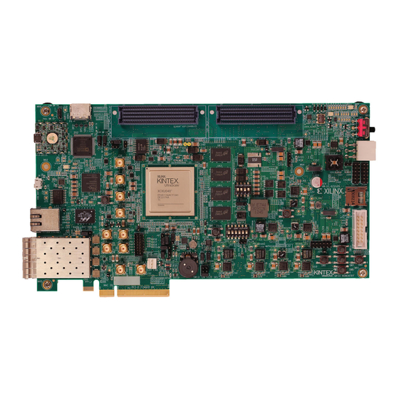
The TRD targets the Kintex® UltraScale™ XCKU040-2FFVA1156E FPGA running on the KCU105 evaluation board and provides a platform for data transfer between the host machine and the FPGA. The top-level block diagram of the TRD base design is shown in Figure 1-1. - Page 6 All other blocks in the hardware design and software components can be reused. UG920_c1_02_040615 Figure 1-2: KCU105 PCI Express Streaming Data Plane User Extension Design The designs delivered as part of this TRD use Vivado® IP integrator to build the system. IP Integrator provides intelligent IP integration in a graphical, Tcl-based, correct-by-construction IP and system-centric design development flow.
-
Page 7: Features
64-bit Linux kernel space drivers for DMA and a raw data driver ° 64-bit Windows 7 drivers for DMA and a raw data driver ° User space application ° Control and monitoring graphical user interface (GUI) ° PCIe Streaming Data Plane TRD www.xilinx.com Send Feedback UG920 (v2017.1) June 01, 2017... -
Page 8: Resource Utilization
Usage (%) CLB registers 484,800 101,313 20.90 CLB LUT 242,400 64,884 26.77 Block RAM 13.33 MMCME3_ADV Global Clock Buffers 1.25 BUFG_GT 10.00 4.42 SYSMONE1 PCIE_3_1 33.33 GTHE3_CHANNEL PCIe Streaming Data Plane TRD www.xilinx.com Send Feedback UG920 (v2017.1) June 01, 2017... -
Page 9: Chapter 2: Setup
Requirements Hardware Board and Peripherals • KCU105 board with the Kintex® UltraScale™ XCKU040-2FFVA1156E FPGA • USB cable, standard-A plug to micro-B plug (Digilent cable) • Power supply: 100 VAC–240 VAC input, 12 VDC 5.0A output •... -
Page 10: Preliminary Setup
Download the Targeted Reference Design Files 1. Download rdf0307-kcu105-trd03-2017-1.zip from the Xilinx Kintex UltraScale FPGA KCU105 Evaluation Kit - Documentation & Designs website. This ZIP file contains the hardware design, software drivers, and application GUI executables. 2. Extract the contents of the file to a working directory. - Page 11 Chapter 2: Setup X-Ref Target - Figure 2-1 UG920_c2_01_040915 Figure 2-1: Disable Driver Signature Enforcement PCIe Streaming Data Plane TRD www.xilinx.com Send Feedback UG920 (v2017.1) June 01, 2017...
- Page 12 6. After installation is complete, click Finish to exit the InstallShield Wizard. Set DIP Switches Ensure that the DIP switches and jumpers on the KCU105 board are set to the factory default settings as identified in the Kintex UltraScale FPGA KCU105 Evaluation Board User...
- Page 13 1. Remove all rubber feet and standoffs from the KCU105 board. 2. Power down the host chassis and disconnect the power cord. Remove the power cord to prevent electrical shock or damage to the KCU105 board or other CAUTION! components.
- Page 14 X-Ref Target - Figure 2-4 UG920_c3_02_061915 Figure 2-4: Power Supply Connection to the KCU105 Board 7. Slide the KCU105 board power switch SW1 to the ON position (ON/OFF is marked on the board). PCIe Streaming Data Plane TRD www.xilinx.com Send Feedback...
-
Page 15: Chapter 3: Bringing Up The Design
2. Place the Fedora 20 LiveDVD into the DVD drive. 3. Select the option to boot from DVD. Complete the Configure the FPGA procedures before exiting the BIOS setup to boot from the DVD. PCIe Streaming Data Plane TRD www.xilinx.com Send Feedback UG920 (v2017.1) June 01, 2017... -
Page 16: Configure The Fpga
Configure the FPGA While in BIOS, program the FPGA with the BIT file. 1. Connect the standard-A plug to micro-B plug USB cable to the JTAG port on the KCU105 board and to the control computer laptop as shown in Figure 3-1. - Page 17 Bringing Up the Design 2. Launch the Vivado® Integrated Design Environment (IDE) on the control computer: a. Select Start > All Programs > Xilinx Design Tools > Vivado 2017.1 > Vivado 2017.1. b. On the getting started page, click Open Hardware Manager (Figure 3-2).
- Page 18 Chapter 3: Bringing Up the Design 3. Open the connection wizard to initiate a connection to the KCU105 board: a. Click Open target > Auto connect (Figure 3-3). X-Ref Target - Figure 3-3 Figure 3-3: Using the User Assistance Bar to Open a Hardware Target PCIe Streaming Data Plane TRD www.xilinx.com...
- Page 19 Chapter 3: Bringing Up the Design 4. Configure the wizard to establish connection with the KCU105 board by selecting the default value on each wizard page. Click Next > Next > Next > Finish. a. In the hardware view, right-click xcku040 and click Program Device (Figure 3-4).
- Page 20 5. After the FPGA is programmed, the DONE LED status should illuminate as shown in Figure 3-6. X-Ref Target - Figure 3-6 UG920_c3_08_092414 Figure 3-6: GPIO LED Indicators PCIe Streaming Data Plane TRD www.xilinx.com Send Feedback UG920 (v2017.1) June 01, 2017...
- Page 21 If the PCIe Endpoint is not discovered, reboot the system. Do not power off. ° 8. Check the status of the design by looking at the GPIO LEDs positioned at the top right corner of the KCU105 board (see Figure 3-6). After FPGA configuration, the LED status...
-
Page 22: Run The Design On The Host Computer
$ lspci | grep Xilinx The following is displayed: 04:00.0 Communications controller: Xilinx Corporation Device 8082 If the host computer does not detect the Xilinx PCIe Endpoint, does not show a lspci Note: Xilinx device. - Page 23 (This takes you to the Control & Monitoring GUI shown in Figure 3-12.) X-Ref Target - Figure 3-8 UG920_c3_10_041615 Figure 3-8: TRD Setup Screen with a PCIe Device Detected PCIe Streaming Data Plane TRD www.xilinx.com Send Feedback UG920 (v2017.1) June 01, 2017...
- Page 24 2. Open Device Manager (click Start > devmgmt.msc then press Enter) and look for the Xilinx PCI Express device as shown in Figure 3-9. X-Ref Target - Figure 3-9 UG920_c3_11_042815 Figure 3-9: Xilinx PCI Express Device in Device Manager PCIe Streaming Data Plane TRD www.xilinx.com Send Feedback UG920 (v2017.1) June 01, 2017...
- Page 25 Bringing Up the Design 3. Open the command prompt with administrator privileges, as shown in Figure 3-10. X-Ref Target - Figure 3-10 UG920_c3_12_041415 Figure 3-10: Command Prompt with Administrator Privileges PCIe Streaming Data Plane TRD www.xilinx.com Send Feedback UG920 (v2017.1) June 01, 2017...
- Page 26 TRD Setup screen. Click Proceed to test the reference design. (This takes you to the Control & Monitoring GUI shown in Figure 3-12.) X-Ref Target - Figure 3-11 UG920_c3_13_042015 Figure 3-11: TRD Setup Screen PCIe Streaming Data Plane TRD www.xilinx.com Send Feedback UG920 (v2017.1) June 01, 2017...
-
Page 27: Test The Reference Design
Click Start to initiate the test. To stop the test, click Stop. (The Start button changes to Stop after the test is initiated). The packet size for all the above modes can be between 64 bytes and 32768 bytes. PCIe Streaming Data Plane TRD www.xilinx.com Send Feedback UG920 (v2017.1) June 01, 2017... - Page 28 Bringing Up the Design X-Ref Target - Figure 3-13 UG920_c3_15_061915 Figure 3-13: System to Card Performance X-Ref Target - Figure 3-14 UG920_c3_16_061915 Figure 3-14: Card to System Performance PCIe Streaming Data Plane TRD www.xilinx.com Send Feedback UG920 (v2017.1) June 01, 2017...
- Page 29 Chapter 3: Bringing Up the Design X-Ref Target - Figure 3-15 UG920_c3_17_061915 Figure 3-15: System to Card and Card to System Performance Together PCIe Streaming Data Plane TRD www.xilinx.com Send Feedback UG920 (v2017.1) June 01, 2017...
- Page 30 You can view the block diagram by clicking Block Diagram in top right corner of the screen (Figure 3-16). X-Ref Target - Figure 3-16 Software Components UG920_c3_18_042015 Figure 3-16: Block Diagram View PCIe Streaming Data Plane TRD www.xilinx.com Send Feedback UG920 (v2017.1) June 01, 2017...
- Page 31 TRD Setup screen. Any files copied or icons created in a Linux machine are not present after the next Fedora 20 Note: LiveDVD boot. PCIe Streaming Data Plane TRD www.xilinx.com Send Feedback UG920 (v2017.1) June 01, 2017...
-
Page 32: Remove Drivers From The Host Computer
Bringing Up the Design Remove Drivers from the Host Computer (Windows Only) Shutdown the host computer and power off the KCU105 board. Then use the following IMPORTANT: steps to remove the Windows drivers. 1. Power on the host computer, and from Windows Explorer, navigate to the folder in which the reference design is downloaded (<dir>\kcu105_axis_dataplane\software\windows\). -
Page 33: Chapter 4: Implementing And Simulating The Design
4. To run the implementation flow in GUI mode, enter: $ vivado -source trd03_base.tcl This opens the Vivado Integrated Design Environment (IDE), loads the block diagram, and adds the required top file and Xilinx design constraints (XDC) file to the project (see Figure 4-1). - Page 34 Chapter 4: Implementing and Simulating the Design X-Ref Target - Figure 4-1 UG920_c4_01_0411175 Figure 4-1: Base Design – Project View PCIe Streaming Data Plane TRD www.xilinx.com Send Feedback UG920 (v2017.1) June 01, 2017...
- Page 35 No Implementation Results are available is displayed. The BIT file can be found under the following directory: kcu105_axis_dataplane/hardware/vivado/runs_base/trd03_base.runs/ impl_1 AXIS represents AXI Streaming. Note: X-Ref Target - Figure 4-2 UG920_c4_02_041117 Figure 4-2: Base Design – Generate Bitstream PCIe Streaming Data Plane TRD www.xilinx.com Send Feedback UG920 (v2017.1) June 01, 2017...
-
Page 36: Implementing The User Extension Design
This opens the Vivado IDE, loads the block diagram, and adds the required top file and XDC file to the project (see Figure 4-3). X-Ref Target - Figure 4-3 UG920_c4_03_041117 Figure 4-3: User Extension Design – Project View PCIe Streaming Data Plane TRD www.xilinx.com Send Feedback UG920 (v2017.1) June 01, 2017... - Page 37 4-4). The generated bitstream can be found under the following directory: kcu105_axis_dataplane/hardware/vivado/runs_2x10g/trd03_2x10g.run s/impl_1 X-Ref Target - Figure 4-4 UG920_c4_04_041117 Figure 4-4: User Extension Design – Generate Bitstream PCIe Streaming Data Plane TRD www.xilinx.com Send Feedback UG920 (v2017.1) June 01, 2017...
-
Page 38: Simulating The Designs Using Vivado Simulator
4-5). This generates all the simulation files, loads the Vivado simulator, and runs the simulation. The result is shown in Figure 4-6. X-Ref Target - Figure 4-5 UG920_c4_05_041117 Figure 4-5: Run Behavioral Simulation PCIe Streaming Data Plane TRD www.xilinx.com Send Feedback UG920 (v2017.1) June 01, 2017... - Page 39 5. To simulate the user extension Ethernet design enter: $ vivado -source trd03_2x10g_xsim.tcl This command opens the Vivado IDE, loads the block diagram, and adds the required top file. PCIe Streaming Data Plane TRD www.xilinx.com Send Feedback UG920 (v2017.1) June 01, 2017...
- Page 40 Behavioral Simulation. This generates all the simulation files, loads Vivado simulator, and runs the simulation. The result is shown in Figure 4-7. X-Ref Target - Figure 4-7 UG920_c4_07_041117 Figure 4-7: Ethernet Design Vivado Simulation PCIe Streaming Data Plane TRD www.xilinx.com Send Feedback UG920 (v2017.1) June 01, 2017...
-
Page 41: Chapter 5: Targeted Reference Design Details And Modifications
TRD hardware design components. Subsequent sections discuss each of the components in detail. X-Ref Target - Figure 5-1 UG920_c5_01_021715 Figure 5-1: TRD Functional Block Diagram PCIe Streaming Data Plane TRD www.xilinx.com Send Feedback UG920 (v2017.1) June 01, 2017... - Page 42 For example, assume that the PCIe BAR2 physical address is 0x2E000000. A memory read request targeted to address 0x2E000000 is translated to 0x44A00000. Table 5-1: Address Translation Maps Ingress Source Base Ingress Destination Base Aperture Size BAR2 0x44A00000 PCIe Streaming Data Plane TRD www.xilinx.com Send Feedback UG920 (v2017.1) June 01, 2017...
- Page 43 DST-Q provides destination buffer information and corresponding STAD-Q which indicates DST-Q processing completion by DMA The queue element layout is depicted in Figure 5-2. X-Ref Target - Figure 5-2 Figure 5-2: SGL Queue Element Structure PCIe Streaming Data Plane TRD www.xilinx.com Send Feedback UG920 (v2017.1) June 01, 2017...
- Page 44 In the C2S direction, host software manages DST-Q and STAD-Q elements. SRC-Q elements are provided by the hardware logic (through the SGL interface) based on incoming data received from the AXI-Stream application. There is no STAS-Q involved. PCIe Streaming Data Plane TRD www.xilinx.com Send Feedback UG920 (v2017.1) June 01, 2017...
- Page 45 The interconnect is responsible for: • Converting AXI3 transactions from the AXI-PCIe bridge into AXI4 transactions for various slaves • Decoding address to target the appropriate slave PCIe Streaming Data Plane TRD www.xilinx.com Send Feedback UG920 (v2017.1) June 01, 2017...
- Page 46 DMA channels. This is useful in a FIFO mode of operation. The logic designed handles both S2C and C2S traffic scenarios. X-Ref Target - Figure 5-5 Figure 5-5: Hardware SGL Interfacing PCIe Streaming Data Plane TRD www.xilinx.com Send Feedback UG920 (v2017.1) June 01, 2017...
- Page 47 The SGL submission logic communicates with the SGL preparation logic using a ready-acknowledge handshaking mechanism. The handshaking protocol for communicating with the DMA SGL interface happens in two phases: PCIe Streaming Data Plane TRD www.xilinx.com Send Feedback UG920 (v2017.1) June 01, 2017...
- Page 48 The second timer waits on the acknowledgment from the DMA SGL interface while the submission block submits the SGL elements to DMA. If a timeout occurs, the submission block flags an error to the preparation logic. PCIe Streaming Data Plane TRD www.xilinx.com Send Feedback UG920 (v2017.1) June 01, 2017...
- Page 49 The hardware SGL Prepare block implements the data memory for temporary data buffering, SGL Prepare logic, and a protocol conversion logic for data conversion from AXI memory-mapped (MM) to AXI-Stream and vice versa. PCIe Streaming Data Plane TRD www.xilinx.com Send Feedback UG920 (v2017.1) June 01, 2017...
- Page 50 Figure 5-8: S2C Prepare Block Diagram The S2C Prepare module consists of following: • Block RAM controller • True dual port block RAM • Read engine • Hardware SGL Prepare block PCIe Streaming Data Plane TRD www.xilinx.com Send Feedback UG920 (v2017.1) June 01, 2017...
- Page 51 After the data size reaches 4096 bytes or end of packet (tlast) occurs (whichever occurs first), builds the SRC-SGL element and submits it to the corresponding DMA channel. • Continues providing SRC_SGL elements as newer data keeps coming into block RAM. PCIe Streaming Data Plane TRD www.xilinx.com Send Feedback UG920 (v2017.1) June 01, 2017...
- Page 52 RAM buffer one after the other, depending on empty buffer availability. The hardware SGL Prepare block prepares an SGL element whenever it sees an end of packet or with the minimum buffer size update (4096 bytes). PCIe Streaming Data Plane TRD www.xilinx.com Send Feedback UG920 (v2017.1) June 01, 2017...
- Page 53 The block provides analog-to-digital conversion and monitoring capabilities. It enables reading of voltage and current on different power supply rails (supported on the KCU105 board) which are then used to calculate power. PCIe Streaming Data Plane TRD www.xilinx.com...
-
Page 54: Data Flow
4. DMA provides data on AXI MM interface as indicated by the DST-Q SGL element. 5. Due to use of a hardware SGL interface, DMA does not fetch DST-Q elements and there is no STAD SGL involved. PCIe Streaming Data Plane TRD www.xilinx.com Send Feedback UG920 (v2017.1) June 01, 2017... -
Page 55: Software
An awareness of the Expresso DMA hardware design and a basic understanding of the PCIe protocol, software engineering fundamentals, and Windows and Linux OS internals are required. PCIe Streaming Data Plane TRD www.xilinx.com Send Feedback UG920 (v2017.1) June 01, 2017... - Page 56 EP, or both host and EP. In this TRD, the scenario of the host software controlling source/destination SGL while EP hardware logic controlling corresponding destination/source SGL is explored. PCIe Streaming Data Plane TRD www.xilinx.com Send Feedback UG920 (v2017.1) June 01, 2017...
- Page 57 This model is typically used where there is hardware logic in the EP that is aware of the Expresso DMA SGL format and operating principles. PCIe Streaming Data Plane TRD www.xilinx.com Send Feedback UG920 (v2017.1) June 01, 2017...
- Page 58 An important attribute of host SGL loc_axi is set to false to indicate to Expresso DMA that the I/O buffer being pointed to by the SGL element is present on the host. PCIe Streaming Data Plane TRD www.xilinx.com Send Feedback UG920 (v2017.1) June 01, 2017...
- Page 59 I/O buffers/FIFOs for data transfer. The XDMA driver on the host and hardware logic on the EP mark the appropriate flag in the buffer descriptor to facilitate data transfer. PCIe Streaming Data Plane TRD www.xilinx.com Send Feedback UG920 (v2017.1) June 01, 2017...
- Page 60 Bridge Initialization: The Expresso IP Core contains a bridge for protocol conversion (AXI to PCIe and vice versa) which needs initialization. The details on bridge initialization are documented under Bridge Initialization, page PCIe Streaming Data Plane TRD www.xilinx.com Send Feedback UG920 (v2017.1) June 01, 2017...
- Page 61 This causes the data to be drained from the EP I/O buffer to the host I/O buffer physical address location 0x880000. The host software is agnostic of the EP memory location PCIe Streaming Data Plane TRD www.xilinx.com Send Feedback UG920 (v2017.1) June 01, 2017...
- Page 62 The application driver can take appropriate action based on the information provided by the DMA driver, such as number of bytes completed or notification of errors (if any) during the transfer. PCIe Streaming Data Plane TRD www.xilinx.com Send Feedback UG920 (v2017.1) June 01, 2017...
- Page 63 APIs for Linux and Appendix E, APIs Provided by the XDMA Driver in Windows for more information on the APIs for Windows. PCIe Streaming Data Plane TRD www.xilinx.com Send Feedback UG920 (v2017.1) June 01, 2017...
- Page 64 An RX thread provides buffers to the DMA ring. • An RX done thread polls for receiving packets. I • A main thread spawns all these threads according to test parameters. PCIe Streaming Data Plane TRD www.xilinx.com Send Feedback UG920 (v2017.1) June 01, 2017...
- Page 65 The GUI periodically polls these statistics from the XDMA driver by opening the driver interface and sending IOCTL system calls. PCIe Streaming Data Plane TRD www.xilinx.com Send Feedback UG920 (v2017.1) June 01, 2017...
- Page 66 DMA TX PORT User PCIe link, DMA Engine Registers and Power Statistics DMA Engine Socket Data Path Flow Control Path Flow Communication Figure 5-13: Control and Data Path Interfaces PCIe Streaming Data Plane TRD www.xilinx.com Send Feedback UG920 (v2017.1) June 01, 2017...
- Page 67 XDMA driver receives a packet. 7. The received packet is queued in the driver. 8. The application periodically polls for receipt of a packet by reading the driver’s queues. PCIe Streaming Data Plane TRD www.xilinx.com Send Feedback UG920 (v2017.1) June 01, 2017...
-
Page 68: Reference Design Modifications
10-Gigabit Ethernet MAC and 10-Gigabit BASE-R PHY are added to convert this design to a dual 10-Gigabit network interface card (NIC). The following section describes the setup procedure required to test the 2x10G Ethernet design in both Application and Performance modes. PCIe Streaming Data Plane TRD www.xilinx.com Send Feedback UG920 (v2017.1) June 01, 2017... - Page 69 FPGA configuration is done and PCIe Endpoint is discovered. The BIT file to be used for this is <working_dir>/kcu105_axis_dataplane/ready_to_test/trd03_2x10g_top.bit. X-Ref Target - Figure 5-14 UG920_c5_14_061915 Figure 5-14: SFP+ Back-to-Back Connection PCIe Streaming Data Plane TRD www.xilinx.com Send Feedback UG920 (v2017.1) June 01, 2017...
- Page 70 Check the status of the design using the KCU105 board LEDs. The design provides status with the GPIO LEDs located on the upper right portion of the KCU105 board. When the PC is powered on and the TRD has successfully configured, the LED status from left to right...
- Page 71 5-16. Make sure to select the Application check box. Click Install. This installs the drivers. X-Ref Target - Figure 5-16 UG920_c5_16_041615 Figure 5-16: Installer Screen for Ethernet Application Design PCIe Streaming Data Plane TRD www.xilinx.com Send Feedback UG920 (v2017.1) June 01, 2017...
- Page 72 Figure 5-17: Control & Monitoring GUI for Ethernet Application 6. Open a terminal with super user permissions and check the IP address for both of the MACs with this command: $ ifconfig PCIe Streaming Data Plane TRD www.xilinx.com Send Feedback UG920 (v2017.1) June 01, 2017...
- Page 73 (NAT) is used to set up the IP address to 10.60.0.1 and 10.60.1.1. This is done during driver installation through scripts. X-Ref Target - Figure 5-19 UG920_c5_19_121614 Figure 5-19: Ethernet Ping Snapshot PCIe Streaming Data Plane TRD www.xilinx.com Send Feedback UG920 (v2017.1) June 01, 2017...
- Page 74 Chapter 5: Targeted Reference Design Details and Modifications 8. The block diagram of the design can be viewed by clicking Block Diagram on the top right corner of the GUI, adjacent to the Xilinx logo (Figure 5-20). X-Ref Target - Figure 5-20...
- Page 75 1. After the PC boots from the Fedora 20 LiveDVD, copy the folder software to the /tmp directory. 2. Log in as super user by typing su on the terminal. 3. Enter cd /tmp/software 4. Enter chmod +x quickstart.sh PCIe Streaming Data Plane TRD www.xilinx.com Send Feedback UG920 (v2017.1) June 01, 2017...
- Page 76 5-22. Make sure to select the Raw Ethernet check box. Click Install. This installs the drivers. X-Ref Target - Figure 5-22 UG920_c5_22_041615 Figure 5-22: Installer Screen for Raw Ethernet PCIe Streaming Data Plane TRD www.xilinx.com Send Feedback UG920 (v2017.1) June 01, 2017...
-
Page 77: Pcie Streaming Data Plane Trd Www.xilinx.com
5-23. Check that the PHY link up LEDs on the GUI are green. X-Ref Target - Figure 5-23 UG920_c5_23_020615 Figure 5-23: Control & Monitoring GUI for Raw Ethernet Data traffic can be started in both datapaths. PCIe Streaming Data Plane TRD www.xilinx.com Send Feedback UG920 (v2017.1) June 01, 2017... - Page 78 Chapter 5: Targeted Reference Design Details and Modifications Figure 5-24 shows the performance with Data Path -0 enabled. X-Ref Target - Figure 5-24 UG920_c5_24_020615 Figure 5-24: Data Path 0 Performance PCIe Streaming Data Plane TRD www.xilinx.com Send Feedback UG920 (v2017.1) June 01, 2017...
- Page 79 Chapter 5: Targeted Reference Design Details and Modifications Figure 5-25 shows the performance with Data Path -1 enabled. X-Ref Target - Figure 5-25 UG920_c5_25_020615 Figure 5-25: Data Path 1 Performance PCIe Streaming Data Plane TRD www.xilinx.com Send Feedback UG920 (v2017.1) June 01, 2017...
- Page 80 Chapter 5: Targeted Reference Design Details and Modifications Figure 5-26 shows performance with both the datapaths enabled. X-Ref Target - Figure 5-26 UG920_c5_26_061915 Figure 5-26: Data Path 0 and 1 Performance PCIe Streaming Data Plane TRD www.xilinx.com Send Feedback UG920 (v2017.1) June 01, 2017...
- Page 81 Chapter 5: Targeted Reference Design Details and Modifications 10. The block diagram of the design can be viewed by clicking Block Diagram on the top right corner of the GUI, adjacent to the Xilinx logo (Figure 5-27). X-Ref Target - Figure 5-27...
- Page 82 12. Click the X mark on the top right corner of GUI to close the GUI. It uninstalls the drivers and returns to the TRD Setup screen (Figure 5-28). X-Ref Target - Figure 5-28 UG920_c5_28_020615 Figure 5-28: Uninstall Device Drivers and Close the Raw Ethernet GUI PCIe Streaming Data Plane TRD www.xilinx.com Send Feedback UG920 (v2017.1) June 01, 2017...
- Page 83 This design demonstrates the use of PCIe Endpoint as a dual 10G Ethernet network interface card (NIC). This design demonstrates movement of Ethernet traffic over PCIe. Two instances of 10GBASE-R PCS-PMA are used with two 10G MACs. This uses the SFP+ interface available on KCU105 (Figure 5-29).
- Page 84 The Ethernet packet length is read from the receive statistics vector instead of implementing a separate counter in logic. PCIe Streaming Data Plane TRD www.xilinx.com Send Feedback UG920 (v2017.1) June 01, 2017...
- Page 85 A pre-built design script is provided for the user extension design which can be run to generate a bitstream. The steps required to build the user extension design are described in Chapter 4, Implementing and Simulating the Design. PCIe Streaming Data Plane TRD www.xilinx.com Send Feedback UG920 (v2017.1) June 01, 2017...
- Page 86 Ethernet flow. The driver fits under the TCP/IP stack software, using the standard hooks provided. 2. The Ethernet driver, through appropriate API calls in the DMA driver, submits the packet in buffer descriptors. PCIe Streaming Data Plane TRD www.xilinx.com Send Feedback UG920 (v2017.1) June 01, 2017...
- Page 87 Ethernet header is programmed as a broadcast message. A packet is transmitted from one network interface and received as a broadcast packet on the other interface. This demonstrates maximum performance in eliminating networking stack overhead. PCIe Streaming Data Plane TRD www.xilinx.com Send Feedback UG920 (v2017.1) June 01, 2017...
-
Page 88: Appendix A: Directory Structure
Table A-1. For a detailed description of each folder, see the Readme file. X-Ref Target - Figure A-1 kcu105_axis_dataplane testbench UG920_aA_01_041415 Figure A-1: TRD Directory Structure PCIe Streaming Data Plane TRD www.xilinx.com Send Feedback UG920 (v2017.1) June 01, 2017... - Page 89 Contains scripts to create a Vivado® Design Suite project and outputs of Vivado tool runs ready to test Contains the BIT files (Base and 2x10G) to program the KCU105 PCI Express Streaming Data Plane application software Contains software design deliverables for Linux and Windows...
-
Page 90: Appendix B: Recommended Practices And Troubleshooting In Windows
1. If the GUI does not detect the board, open Device Manager and see if the drivers are loaded under Xilinx PCI Express Device. 2. If the drivers are not loaded, check the PCIe Link Up LED on the board (see Figure 5-15). - Page 91 Appendix B: Recommended Practices and Troubleshooting in Windows 4. Invoke the GUI of the reference design and check if it detects the board. PCIe Streaming Data Plane TRD www.xilinx.com Send Feedback UG920 (v2017.1) June 01, 2017...
-
Page 92: Appendix C: Register Space
Maximum supported size is 32 KB packets. Table C-5: Checker Length Register (0x44A0_0010) Bit Position Mode Default Value Description 31:0 Packet length to be checked in Checker mode. PCIe Streaming Data Plane TRD www.xilinx.com Send Feedback UG920 (v2017.1) June 01, 2017... -
Page 93: Ethernet Mac Registers
Table C-11: MAC_1 Promiscuous Mode Enable Register (0x44A0_140C) Bit Position Mode Default Value Description 31:1 Read only 0x0000 Reserved MAC_1 Promiscuous mode Enable. Value of 1 enables Promiscuous mode. PCIe Streaming Data Plane TRD www.xilinx.com Send Feedback UG920 (v2017.1) June 01, 2017... - Page 94 15:8 Read only PHY 0 Status. LSB bit represents PHY link up status. 0x00 Read only PHY 1 Status. LSB bit represents PHY link up status. 0x00 PCIe Streaming Data Plane TRD www.xilinx.com Send Feedback UG920 (v2017.1) June 01, 2017...
-
Page 95: Appendix D: Apis Provided By The Xdma Driver In Linux
(stacked on the XDMA driver) during initialization. On the Endpoint side, this API needs to be called just once, because a single XDMA instance is supported. PCIe Streaming Data Plane TRD www.xilinx.com Send Feedback UG920 (v2017.1) June 01, 2017... - Page 96 On failure, a descriptor. XDMA has four acquired from a call to negative value is returned. ps_pcie_dma_desc_t DMA channels. xlnx_get_pform_dma_desc Check “/* Xilinx DMA *ptr_dma_desc, u32 driver status messages */” channel_id, direction_t This API is typically called dir, during initialization by the channel_id –...
- Page 97 _t *ptr_chann_desc, Based on the direction of earlier call to Check “/* Xilinx DMA unsigned int the channel (specified xlnx_get_dma_channel. driver status messages */” *ptr_data_q_addr_hi, during the call to get the ptr_data_q_addr_hi –...
- Page 98 Returns XLNX_SUCCESS xlnx_activate_dma_channe channel for usage. Channel descriptor on success. On failure, a pointer acquired by an negative value is returned. earlier call to Check “/* Xilinx DMA ps_pcie_dma_desc_t xlnx_get_dma_channel driver status messages */” *ptr_dma_desc, ps_pcie_dma_chann_desc data_q_addr_hi – Upper _t *ptr_chann_desc, 32 bits of data queue ps_pcie_dma_driver.
- Page 99 ( across a PCIe link. A pointer negative value is returned. ps_pcie_dma_chann_desc channel lock has to be Check “/* Xilinx DMA addr_buf – Pointer to _t *ptr_chan_desc, held while invoking this driver status messages */” start memory location for unsigned char * API.
- Page 100 ( results in a reset of the pointer negative value is returned. ps_pcie_dma_chann_desc DMA channel. Check “/* Xilinx DMA do_rst – Currently this has _t *ptr_chann_desc, driver status messages */” to be always set to true. bool do_rst); ps_pcie_dma_driver.
-
Page 101: Appendix E: Apis Provided By The Xdma Driver In Windows
Appendix E APIs Provided by the XDMA Driver in Windows Table E-1 describes the application programming interfaces (APIs) provided by the XDMA driver in a Windows environment. PCIe Streaming Data Plane TRD www.xilinx.com Send Feedback UG920 (v2017.1) June 01, 2017... - Page 102 1. DMA function pointer for initiating data transfer. 2. DMA function pointer for cancelling transfers and doing DMA reset. PCIe Streaming Data Plane TRD www.xilinx.com Send Feedback UG920 (v2017.1) June 01, 2017...
- Page 103 3. Memory location information, which helps the DMA driver to know whether the address provided is the Card DDR address or if it is a host SGL list. PCIe Streaming Data Plane TRD www.xilinx.com Send Feedback UG920 (v2017.1) June 01, 2017...
- Page 104 _RETURN upon successful after successful registration. registration of Child driver. Using this API the child driver can cancel all pending transfers and reset the DMA. PCIe Streaming Data Plane TRD www.xilinx.com Send Feedback UG920 (v2017.1) June 01, 2017...
-
Page 105: Appendix F: Network Performance
This runs netperf (TCP_STREAM test for 10 seconds) and targets the server at port 5005. 5. To repeat the same process for 10.60.1.1 IP, set up netserver at a different port, for example, 5006, and repeat the previous steps. PCIe Streaming Data Plane TRD www.xilinx.com Send Feedback UG920 (v2017.1) June 01, 2017... - Page 106 Figure F-1: Private LAN Setup To set up a private LAN connection: 1. Connect two machines that contain the KCU105 board and connect the fiber optic cable between the SFP+ cages on the board. Connect the fiber cable in a 1:1 manner, that is, connect SFP0 of one board to SFP0 of the other board, and connect SFP1 of one board to SFP1 of the other board.
- Page 107 6. Make the other end a client. On a terminal, run netperf: $ netperf -H <IP-address> This runs a ten second TCP_STREAM test by default and reports outbound performance. PCIe Streaming Data Plane TRD www.xilinx.com Send Feedback UG920 (v2017.1) June 01, 2017...
-
Page 108: Appendix G: Additional Resources And Legal Notices
The most up-to-date information for this design is available on these websites: KCU105 Evaluation Kit website KCU105 Evaluation Kit documentation KCU105 Evaluation Kit - Known Issues and Master Answer Record AR 63175 These documents and sites provide supplemental material: 1. Northwest Logic Expresso DMA Bridge Core 2. -
Page 109: Please Read: Important Legal Notices
Xilinx’s Terms of Sale which can be viewed at http://www.xilinx.com/legal.htm#tos; IP cores may be subject to warranty and support terms contained in a license issued to you by Xilinx. Xilinx products are not designed or intended to be fail-safe or for use in any application requiring fail-safe performance;... - Page 110 © Copyright 2014–2017 Xilinx, Inc. Xilinx, the Xilinx logo, Artix, ISE, Kintex, Spartan, Virtex, Vivado, Zynq, and other designated brands included herein are trademarks of Xilinx in the United States and other countries. PCI, PCIe and PCI Express are trademarks of PCI-SIG and used under license.
Need help?
Do you have a question about the KCU105 and is the answer not in the manual?
Questions and answers