Xilinx KC705 User Manual
Evaluation board
for the kintex-7 fpga
Hide thumbs
Also See for KC705:
- User manual (110 pages) ,
- Getting started (24 pages) ,
- User manual (90 pages)

Related Manuals for Xilinx KC705


Summary of Contents for Xilinx KC705
- Page 1 KC705 Evaluation Board for the Kintex-7 FPGA User Guide UG810 (v1.8) March 20, 2018...
-
Page 2: Revision History
Appendix C, Master Constraints File Listing, changed appendix title from Master UCF Listing to Master Board Constraints, replaced references to the term UCF with the term XDC and replaced the KC705 Board UCF Listing with the KC705 Board XDC Listing. - Page 3 80. Added references to Documents, page 85. Added Appendix E, Compliance with European Union Directives and Standards, Appendix D, Board Setup, and Appendix E, Board Specifications. 01/23/2012 Initial Xilinx release. KC705 Evaluation Board Send Feedback UG810 (v1.8) March 20, 2018 www.xilinx.com...
-
Page 4: Table Of Contents
Installing KC705 Board in a PC Chassis ........ - Page 5 Please Read: Important Legal Notices ..........116 KC705 Evaluation Board Send Feedback UG810 (v1.8) March 20, 2018...
-
Page 6: Overview
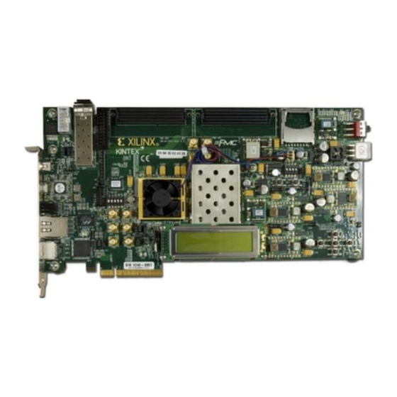
Chapter 1 KC705 Evaluation Board Features Overview The KC705 evaluation board for the Kintex®-7 FPGA provides a hardware environment for developing and evaluating designs targeting the Kintex-7 XC7K325T-2FFG900C FPGA. The KC705 board provides features common to many embedded processing systems, including a DDR3 SODIMM memory, an 8-lane PCI Express®... - Page 7 Chapter 1: KC705 Evaluation Board Features • GTX transceivers FMC HPC connector (four GTX transceivers) ° FMC LPC connector (one GTX transceiver) ° SMA connectors (one pair each for TX, RX, and REFCLK) ° PCI Express (eight lanes) ° Small form-factor pluggable plus (SFP+) connector °...
- Page 8 1-1. The KC705 board schematics are available for download from the Kintex-7 FPGA KC705 Evaluation Kit website. The KC705 board can be damaged by electrostatic discharge (ESD). Follow standard ESD CAUTION! prevention measures when handling the board. KC705 Evaluation Board Send Feedback UG810 (v1.8) March 20, 2018...
-
Page 9: Feature Descriptions
USB Connector UG810_c1_01_011812 Figure 1-1: KC705 Board Block Diagram Feature Descriptions Figure 1-2 shows the KC705 board. Each numbered feature that is referenced in Figure 1-2 is described in the sections that follow. The image in Figure 1-2 is for reference only and might not reflect the current revision of the Note: board. - Page 10 Chapter 1: KC705 Evaluation Board Features X-Ref Target - Figure 1-2 Round callout references a component Square callout references a component on the front side of the board on the back side of the board User rotary switch located under LCD...
- Page 11 Chapter 1: KC705 Evaluation Board Features Table 1-1: KC705 Board Component Descriptions (Cont’d) Schematic Reference Callout Component Description Notes 0381397 Designator Page Number GTX Transceivers Embedded within FPGA U1 PCI Express Edge Connector 8-lane card edge connector SFP/SFP+ Connector Molex 74441-0010...
- Page 12 Master BPI flash memory using the onboard Linear BPI flash memory • JTAG using a standard-A to micro-B USB cable for connecting the host PC to the KC705 board configuration port Each configuration interface corresponds to one or more configuration modes and bus...
- Page 13 For full details on configuring the FPGA, see 7 Series FPGAs Configuration User Guide (UG470) [Ref Encryption Key Backup Circuit FPGA U1 implements bitstream encryption key technology. The KC705 board provides the encryption key backup battery circuit shown in Figure 1-4. The rechargeable 1.5V lithium button-type battery B1 is soldered to the board with the positive output connected to FPGA U1 VCCBATT pin C10.
- Page 14 Chapter 1: KC705 Evaluation Board Features Table 1-3: I/O Voltage Rails U1 FPGA Bank Power Supply Rail Net Name Voltage Bank 0 VCC2V5_FPGA 2.5V Bank 12 VADJ_FPGA 2.5V (default) Bank 13 VADJ_FPGA 2.5V (default) Bank 14 VCC2V5_FPGA 2.5V Bank 15 VCC2V5_FPGA 2.5V...
- Page 15 Chapter 1: KC705 Evaluation Board Features Table 1-4: DDR3 Memory Connections to the FPGA J1 DDR3 Memory U1 FPGA Net Name I/O Standard Pin Name Number AH12 DDR3_A0 SSTL15 AG13 DDR3_A1 SSTL15 AG12 DDR3_A2 SSTL15 AF12 DDR3_A3 SSTL15 AJ12 DDR3_A4...
- Page 16 Chapter 1: KC705 Evaluation Board Features Table 1-4: DDR3 Memory Connections to the FPGA (Cont’d) J1 DDR3 Memory U1 FPGA Net Name I/O Standard Pin Name Number AA18 DDR3_D12 SSTL15 DQ12 AB18 DDR3_D13 SSTL15 DQ13 AE18 DDR3_D14 SSTL15 DQ14 AD18...
- Page 17 Chapter 1: KC705 Evaluation Board Features Table 1-4: DDR3 Memory Connections to the FPGA (Cont’d) J1 DDR3 Memory U1 FPGA Net Name I/O Standard Pin Name Number DDR3_D43 SSTL15 DQ43 DDR3_D44 SSTL15 DQ44 DDR3_D45 SSTL15 DQ45 DDR3_D46 SSTL15 DQ46 DDR3_D47...
- Page 18 CK1_N AE11 DDR3_CLK1_P DIFF_SSTL15 CK1_P The KC705 DDR3 SODIMM interface adheres to the constraints guidelines documented in the DDR3 Design Guidelines section of 7 Series FPGAs Memory Interface Solutions KC705 Evaluation Board Send Feedback UG810 (v1.8) March 20, 2018 www.xilinx.com...
- Page 19 Chapter 1: KC705 Evaluation Board Features User Guide (UG586) [Ref 3]. The KC705 DDR3 SODIMM interface is a 40Ω impedance implementation. Other memory interface details are available in UG586 and 7 Series FPGAs Memory Resources User Guide (UG473) [Ref 4] .
- Page 20 Chapter 1: KC705 Evaluation Board Features Table 1-5: BPI Flash Memory Connections to the FPGA (Cont’d) U58 BPI Flash Memory U1 FPGA Pin Net Name I/O Standard Pin Number Pin Name FLASH_A6 LVCMOS25 FLASH_A7 LVCMOS25 FLASH_A8 LVCMOS25 FLASH_A9 LVCMOS25 FLASH_A10...
- Page 21 Chapter 1: KC705 Evaluation Board Features Table 1-5: BPI Flash Memory Connections to the FPGA (Cont’d) U58 BPI Flash Memory U1 FPGA Pin Net Name I/O Standard Pin Number Pin Name FLASH_D12 LVCMOS25 DQ12 FLASH_D13 LVCMOS25 DQ13 FLASH_D14 LVCMOS25 DQ14...
- Page 22 Chapter 1: KC705 Evaluation Board Features Figure 1-5 shows the connections of the linear BPI flash memory on the KC705 board. For more information about the Micron PC28F00AP30TF part, see [Ref X-Ref Target - Figure 1-5 PC28F00AP30TF 64-Pin BGA (8 x 10 mm)
- Page 23 Chapter 1: KC705 Evaluation Board Features Quad SPI Flash Memory [Figure 1-2, callout 4] The Quad SPI flash memory located at U7 on the back side of the board provides 128 Mb of nonvolatile storage that can be used for configuration and data storage.
- Page 24 [Figure 1-2, callout 5] The KC705 board includes a secure digital input/output (SDIO) interface to provide user-logic access to general purpose nonvolatile SDIO memory cards and peripherals. The SD card slot is designed to support 50 MHz high speed SD cards.
- Page 25 Chapter 1: KC705 Evaluation Board Features and the SD card connector (U9). Figure 1-7 shows the connections of the SD card interface on the KC705 board. X-Ref Target - Figure 1-7 VCC3V3 VCC3V3 VADJ VCC3V3 51.1K 1% Six Places 51.1K 1% Six Places 0.1μF 25V...
- Page 26 UG810_c1_08_031214 Figure 1-8: JTAG Chain Block Diagram When an FMC card is attached to the KC705 board, it is automatically added to the JTAG chain through electronically controlled single-pole single-throw (SPST) switches U76 and U77. The SPST switches are in a normally closed state and transition to an open state when an FMC mezzanine card is attached.
- Page 27 Chapter 1: KC705 Evaluation Board Features configures the FPGA with a temporary design to access and program the BPI or Quad SPI flash memory device. The JTAG circuit is shown in Figure 1-9. X-Ref Target - Figure 1-9 VCC3V3 VCC3V3...
-
Page 28: Clock Generation
Chapter 1: KC705 Evaluation Board Features Clock Generation There are five clock sources available for the FPGA fabric on the KC705 board (refer to Table 1-8). Table 1-8: KC705 Board Clock Sources Clock Name Reference Description System Clock SiT9102 2.5V LVDS 200 MHz Fixed Frequency Oscillator (Si Time). See... - Page 29 156.250 MHz. User applications can change the output frequency within the range of 10 MHz to 810 MHz through an I2C interface. Power cycling the KC705 board reverts the user clock to its default frequency of 156.250 MHz.
- Page 30 [Ref 9] • XTP187, KC705 Si570 Fixed Frequencies [Ref 10] • RDF0176, KC705 Si570 Fixed Frequencies Design Files [Ref 11] User SMA Clock Input [Figure 1-2, callout 9] An external high-precision clock signal can be provided to the FPGA bank 15 by connecting differential clock signals through the onboard 50Ω...
- Page 31 [Figure 1-2, callout 10] The KC705 board includes a pair of SMA connectors for a GTX clock wired to GTX Quad bank 117. This differential clock has signal names SMA_MGT_REFCLK_P and SMA_REFCLK_N, which are connected to FPGA U1 pins J8 and J7 respectively.
- Page 32 [Figure 1-2, callout 11] The KC705 board includes a Silicon Labs Si5324 jitter attenuator U70 on the back side of the board. FPGA user logic can implement a clock recovery circuit and then output this clock to a differential I/O pair on I/O bank 13 (REC_CLOCK_C_P, FPGA U1 pin W27 and REC_CLOCK_C_N, FPGA U1 pin W28) for jitter attenuation.
- Page 33 For more information about the Silicon Labs Si5324 see [Ref GTX Transceivers [Figure 1-2, callout 12] The KC705 board provides access to 16 GTX transceivers: • Eight of the GTX transceivers are wired to the PCI Express® x8 endpoint edge connector (P1) fingers •...
- Page 34 The GTX transceivers in 7 series FPGAs are grouped into four channels described as Quads. The reference clock for a Quad can be sourced from the Quad above or Quad below the GTX Quad of interest. There are four GTX Quads on the KC705 board with connectivity as shown here: •...
- Page 35 85Ω ±10%. The PCIe clock is routed as a 100Ω differential pair. The 7 series FPGAs GTX transceivers are used for multi-gigabit per second serial interfaces. The XC7K325T-2FFG900C FPGA (-2 speed grade) included with the KC705 board supports up to Gen2 x8. KC705 Evaluation Board Send Feedback UG810 (v1.8) March 20, 2018...
- Page 36 Chapter 1: KC705 Evaluation Board Features The PCIe clock is input from the edge connector. It is AC coupled to the FPGA through the MGTREFCLK1 pins of Quad 115. PCIE_CLK_Q0_P is connected to FPGA U1 pin U8, and the _N net is connected to pin U7.
- Page 37 Chapter 1: KC705 Evaluation Board Features Table 1-11: PCIe Edge Connector Connections (Cont’d) PCIe Edge Schematic Net FPGA Pin PCIe Edge Connector Function FFG900 Placement Name (U1) Pin Name PCIE_RX3_N PETn3 Integrated Endpoint block GTXE2_CHANNEL_X0Y4 receive pair PCIE_RX4_P PETp4 Integrated Endpoint block...
- Page 38 Chapter 1: KC705 Evaluation Board Features Table 1-11: PCIe Edge Connector Connections (Cont’d) PCIe Edge Schematic Net FPGA Pin PCIe Edge Connector Function FFG900 Placement Name (U1) Pin Name PCIE_TX5_P PERp5 Integrated Endpoint block GTXE2_CHANNEL_X0Y2 transmit pair PCIE_TX5_N PERn5 Integrated Endpoint block...
- Page 39 Chapter 1: KC705 Evaluation Board Features Table 1-12: GTX Quad 115 PCIe Edge Connector Connections (Cont’d) PCIe Edge FPGA PCIe Edge Quad 115 Pin Name Schematic Net Name Connector FFG900 Placement Pin (U1) Pin Name MGTXTXP2_115_U4 PCIE_TX5_P PERp5 GTXE2_CHANNEL_X0Y2 MGTXTXN2_115_U3...
- Page 40 Chapter 1: KC705 Evaluation Board Features Table 1-13: GTX Quad 116 to PCIe Edge Connector Connections (Cont’d) PCIe Edge PCIe FPGA Quad 116 Pin Name Schematic Net Name Connector Edge in FFG900 Placement Pin (U1) Name MGTXRXP2_116_P6 PCIE_RX1_P PETp1 GTXE2_CHANNEL_X0Y6...
- Page 41 Chapter 1: KC705 Evaluation Board Features SFP/SFP+ Connector [Figure 1-2, callout 14] The KC705 board contains a small form-factor pluggable (SFP+) connector and cage assembly that accepts SFP or SFP+ modules. Figure 1-17 shows the SFP+ module connector circuitry. X-Ref Target - Figure 1-17...
- Page 42 TX_DISABLE Notes: 1. On KC705 boards prior to Rev 1.1, SFP+ connector P5 pin 18 RD_P is connected to net SFP_RX_N, and pin 19 RD_N is connected to net SFP_RX_P. 2. On KC705 boards prior to Rev 1.1, SFP+ connector P5 pin 18 TD_P is connected to net SFP_TX_N, and pin 19 TD_N is connected to net SFP_TX_P.
- Page 43 10/100/1000 Tri-Speed Ethernet PHY [Figure 1-2, callout 15] The KC705 board utilizes the Marvell Alaska PHY device (88E1111) U37 for Ethernet communications at 10, 100, or 1000 Mb/s. The board supports MII, GMII, RGMII, and SGMII interfaces from the FPGA to the PHY (Table 1-16).
- Page 44 Chapter 1: KC705 Evaluation Board Features SGMII GTX Transceiver Clock Generator [Figure 1-2, callout 16] An Integrated Circuit Systems ICS844021I chip (U2) generates a high-quality, low-jitter, 125 MHz LVDS clock from a 25 MHz crystal (X3). This clock is sent to FPGA U1, bank 117 GTX transceiver (clock pins G8 (P) and G7 (N)) driving the SGMII interface.
- Page 45 The KC705 board contains a Silicon Labs CP2103GM USB-to-UART bridge device (U12) which allows a connection to a host computer with a USB port. The USB cable is supplied in the Evaluation Kit (standard-A plug to host computer, mini-B plug to KC705 board KC705 Evaluation Board Send Feedback UG810 (v1.8) March 20, 2018...
- Page 46 USB cable is plugged into the USB port on the KC705 board. Xilinx UART IP is expected to be implemented in the FPGA fabric. The FPGA supports the USB-to-UART bridge using four signal pins: Transmit (TX), Receive (RX), Request to Send (RTS), and Clear to Send (CTS).
- Page 47 [Figure 1-2, callout 18] The KC705 board provides a High-Definition Multimedia Interface (HDMI) video output using the Analog Devices ADV7511KSTZ-P HDMI transmitter (U65). The HDMI output is provided on a Molex 500254-1927 HDMI type-A connector (P6). The ADV7511 is wired to support 1080P 60Hz, YCbCr 4:2:2 encoding via 16-bit input data mapping.
- Page 48 Chapter 1: KC705 Evaluation Board Features Figure 1-19 shows the HDMI codec circuit. X-Ref Target - Figure 1-19 VCC3V3 VADJ VCC2V5 R388 R435 2.43K 2.43K SIT8102 R389 1/10W 1/10W 12.00000 MHZ 2.43K R607 50PPM 1/10W ADV7511 24.9 HDMI_INT 1/10W HDMI_CEC_CLK_R...
- Page 49 Chapter 1: KC705 Evaluation Board Features Table 1-21 lists the connections between the codec and the FPGA. Table 1-21: FPGA to HDMI Codec Connections (ADV7511) ADV7511 (U65) U1 FPGA Pin Schematic Net Name I/O Standard Pin Number Pin Name HDMI_D0...
- Page 50 For more information about the ADV7511KSTZ-P part, see [Ref 17]. LCD Character Display [Figure 1-2, callout 19] A 2-line by 16-character display is provided on the KC705 board (Figure 1-20). X-Ref Target - Figure 1-20 LCD Display (16 x 2) UG810_c1_20_031214...
- Page 51 UG810_c1_21_031214 Figure 1-21: LCD Interface Circuit The KC705 board base board uses a male Samtec MTLW-107-07-G-D-265 2x7 header (J31) with 0.025-inch square posts on 0.100-inch centers for connecting to a Samtec SLW-107-01-L-D female socket on the LCD display panel assembly. The LCD header shown Figure 1-22.
- Page 52 [Figure 1-2, callout 20] The KC705 board implements a single I2C port on the FPGA (IIC_SDA_MAIN, IIC_SDA_SCL), which is routed through a TI PCA9548 1-to-8 channel I2C switch (U49). U49 pin 24 net IIC_MUX_RESET_B is connected to U1 bank 15 pin P23. This is an active-Low signal and must be driven High (FPGA U1 pin P23) to enable I2C bus transactions between the FPGA U1 and the other components on the I2C bus.
-
Page 53: Status Leds
Chapter 1: KC705 Evaluation Board Features Table 1-24 lists the address for each device on the I2C bus. Table 1-24: I2C Devices I2C Switch I2C Device I2C Address Position Si570 Clock 0b1011101 FMC HPC 0bXXXXXXX FMC LPC 0bXXXXXXX IIC EEPROM... - Page 54 The Ethernet PHY status LEDs are mounted to be visible through the metal bracket on the left edge of the KC705 board when it is installed into a PCIe slot in a PC chassis. The six PHY status LEDs are located above the RJ45 Ethernet jack as shown in Figure 1-24.
- Page 55 Chapter 1: KC705 Evaluation Board Features GPIO_SW_[NESWC]: SW2, SW3, SW4, SW6, SW5 ° CPU_RESET: SW7 ° • 4-position user DIP Switch (callout 24) GPIO_DIP_SW[3:0]: SW11 ° • User Rotary Switch (callout 25, hidden beneath the LCD) ROTARY_PUSH, ROTARY_INCA, ROTARY_INCB: SW8 °...
- Page 56 Chapter 1: KC705 Evaluation Board Features User Pushbuttons [Figure 1-2, callout 23] Figure 1-26 shows the user pushbutton switch circuits. X-Ref Target - Figure 1-26 VCC1V5 GPIO SW N 4.7kΩ 0.1 W VCC1V5 VADJ VCC1V5 GPIO SW W GPIO SW C GPIO SW E 4.7kΩ...
- Page 57 Chapter 1: KC705 Evaluation Board Features CPU Reset Pushbutton [Figure 1-2, callout 37] Figure 1-27 shows the CPU reset pushbutton circuit. X-Ref Target - Figure 1-27 VCC1V5 CPU_RESET 4.7kΩ 0.1 W UG810_c1_27_031214 Figure 1-27: CPU Reset Pushbutton GPIO DIP Switch...
- Page 58 Chapter 1: KC705 Evaluation Board Features Rotary Switch Figure 1-29 shows the rotary switch SW8. [Figure 1-2, callout 25] X-Ref Target - Figure 1-29 Edge Drive Jog Encoder EVQ-WK4001 ROTARY INCB ROTARY PUSH SW1B SW1A ROTARY INCA 4.7K 4.7K 4.7K...
- Page 59 Chapter 1: KC705 Evaluation Board Features GPIO SMA Connectors Figure 1-30 shows the GPIO SMAs J13 and J14. [Figure 1-2, callout 26] X-Ref Target - Figure 1-30 USER SMA GPIO P Connector USER SMA GPIO N Connector UG885_c1_30_031214 Figure 1-30: GPIO SMAs J13 and J14 Table 1-27 lists the GPIO Connections to FPGA U1.
- Page 60 [Figure 1-2, callout 27] The KC705 board power switch is SW15. Sliding the switch actuator from the Off to On position applies 12V power from J49, a 6-pin mini-fit connector. Green LED DS22 illuminates when the KC705 board power is on. See...
- Page 61 Chapter 1: KC705 Evaluation Board Features Do NOT plug a PC ATX power supply 6-pin connector into J49 on the KC705 board The ATX CAUTION! 6-pin connector has a different pinout than J49. Connecting an ATX 6-pin connector into J49 will damage the KC705 board and void the board warranty.
- Page 62 Chapter 1: KC705 Evaluation Board Features Figure 1-33 shows SW14. X-Ref Target - Figure 1-33 VCC2V5 R295 4.7kΩ 0.1 W SW14 FPGA_PROG_B UG810_c1_33_031214 Figure 1-33: FPGA_PROG_B Pushbutton SW14 Configuration Mode and Upper Linear Flash Address Switch (SW13) [Figure 1-2, callout 29] FPGA Configuration Mode: DIP switch SW13 positions 3, 4, and 5 control which configuration mode is used at power-up or when the PROG pushbutton is pressed.
- Page 63 1-2, callout - 31] The KC705 evaluation board for the Kintex-7 FPGA supports the VITA 57.1 FPGA Mezzanine Card (FMC) specification by providing subset implementations of a high pin count (HPC) connector at J22 and a low pin count (LPC) connector at J2. Both connectors use the same 10 x 40 form factor, except the HPC version is fully populated with 400 pins and the LPC version is partially populated with 160 pins.
- Page 64 The HPC signals are distributed across GTX Quads 116, 117, and 118. Each of these Quads have their VCCO voltage connected to VADJ. The KC705 board VADJ voltage for the J22 and J2 connectors is determined by the FMC VADJ Note:...
- Page 65 Chapter 1: KC705 Evaluation Board Features Table 1-28: HPC Connections, J22 to FPGA U1 (Cont’d) FPGA FPGA J22 Pin Schematic Net Name J22 Pin Schematic Net Name Standard U1 Pin Standard U1 Pin FMC_HPC_DP0_C2M_P PWRCTL1_VCC4A_PG FMC_HPC_DP0_C2M_N FMC_HPC_GBTCLK0_M2C_P LVDS FMC_HPC_DP0_M2C_P FMC_HPC_GBTCLK0_M2C_N...
- Page 66 Chapter 1: KC705 Evaluation Board Features Table 1-28: HPC Connections, J22 to FPGA U1 (Cont’d) FPGA FPGA J22 Pin Schematic Net Name J22 Pin Schematic Net Name Standard U1 Pin Standard U1 Pin FMC_HPC_HA09_P LVDS FMC_HPC_HA04_N LVDS FMC_HPC_HA09_N LVDS FMC_HPC_HA08_P...
- Page 67 Chapter 1: KC705 Evaluation Board Features Table 1-28: HPC Connections, J22 to FPGA U1 (Cont’d) FPGA FPGA J22 Pin Schematic Net Name J22 Pin Schematic Net Name Standard U1 Pin Standard U1 Pin FMC_HPC_LA12_P LVDS FMC_HPC_LA07_P LVDS FMC_HPC_LA12_N LVDS FMC_HPC_LA07_N...
- Page 68 Chapter 1: KC705 Evaluation Board Features Table 1-28: HPC Connections, J22 to FPGA U1 (Cont’d) FPGA FPGA J22 Pin Schematic Net Name J22 Pin Schematic Net Name Standard U1 Pin Standard U1 Pin FMC_HPC_HA22_P LVDS FMC_HPC_HA21_N LVDS FMC_HPC_HA22_N LVDS FMC_HPC_HA23_P...
- Page 69 Chapter 1: KC705 Evaluation Board Features • 2 differential clocks • 61 ground and 9 power connections Table 1-29: LPC Connections, J2 to FPGA U1 J2 Pin Schematic Net Name FPGA Schematic Net Name FPGA Standard Standard FMC_LPC_DP0_C2M_P PWRCTL1_VCC4A_PG FMC_LPC_DP0_C2M_N...
- Page 70 Chapter 1: KC705 Evaluation Board Features Table 1-29: LPC Connections, J2 to FPGA U1 (Cont’d) J2 Pin Schematic Net Name FPGA Schematic Net Name FPGA Standard Standard FMC_LPC_CLK1_M2C_N LVDS AH29 FMC_LPC_PRSNT_M2C_B LVCMOS25 FMC_LPC_LA00_CC_P LVCOMS1 AD23 FMC_LPC_CLK0_M2C_P LVDS AF22 FMC_LPC_LA00_CC_N LVCOMS1...
-
Page 71: Power Management
[Figure 1-2, callout 32] The KC705 board uses power regulators and PMBus compliant digital PWM system controllers from Texas Instruments to supply core and auxiliary voltages. The Texas Instruments Fusion Digital Power graphical user interface (GUI) is used to monitor the current and temperature levels of the board power modules. - Page 72 Chapter 1: KC705 Evaluation Board Features The KC705 board power distribution diagram is shown in Figure 1-35. X-Ref Target - Figure 1-35 VCC12_P Power Plane Power Controller 1 (Core) From SW15 U55 Address 52 VCCINT Switching Regulator 1.0V at 20A...
- Page 73 Chapter 1: KC705 Evaluation Board Features The KC705 board core and auxiliary voltages are listed in Table 1-30. Table 1-30: Onboard Power System Devices Reference Power Rail Net Power Rail Schematic Device Type Description Designator Name Voltage Page Core Voltage Controller and Regulators...
- Page 74 1-33. FMC_VADJ Voltage Control The FMC_VADJ rail is set to 2.5V. When the KC705 board is powered on, the state of the FMC_VADJ_ON_B signal wired to header J65 is sampled by the Texas Instruments UCD9248 controller U55. If a jumper is installed on J65, signal FMC_VADJ_ON_B is held low, and the TI controller U55 energizes the FMC_VADJ rail at power on.
- Page 75 Chapter 1: KC705 Evaluation Board Features X-Ref Target - Figure 1-36 VCC12_P R392 R393 10.0K 1% 10.0K 1% 1/10W 1/10W SM_FAN_TACH FPGA Fan Tach U1 Pin U22 Cooling Fan +12V R390 2.7V 4.75K 1% Fan GND 500 mW 100V 1/10W...
- Page 76 Chapter 1: KC705 Evaluation Board Features Table 1-31 defines the voltage and current values for each power rail controlled by the UCD9248 PMBus controller at Address 52 (U55). Table 1-31: Power Rail Specifications for UCD9248 PMBus controller at Address 52...
- Page 77 Chapter 1: KC705 Evaluation Board Features Table 1-32: Power Rail Specifications for UCD9248 PMBus controller at Address 53 (Cont’d) Shutdown Threshold Rail Rail Schematic Number Name Rail Name Rail #4 MGTAVTT 1.08 1.02 1.38 10.41 Notes: 1. The values defined in these columns are the voltage, current, and temperature thresholds that cause the regulator to shut down if the value is exceeded.
- Page 78 UG810_c1_37_031214 Figure 1-37: Header XADC_VREF Voltage Source Options The KC705 board supports both the internal FPGA sensor measurements and the external measurement capabilities of the XADC. Internal measurements of the die temperature, VCCINT, VCCAUX, and VCCBRAM are available. The KC705 board VCCINT and VCCBRAM are provided by a common 1.0 V supply.
- Page 79 Chapter 1: KC705 Evaluation Board Features Jumper J47 can be used to select either an external differential voltage reference (XADC_VREF) or on-chip voltage reference (jumper J47 2–3) for the analog-to-digital converter. For external measurements an XADC header (J46) is provided. This header can be used to provide analog inputs to the FPGA dedicated VP/VN channel, and to the VAUXP[0]/VAUXN[0], VAUXP[8]/VAUXN[8] auxiliary analog input channels.
-
Page 80: Configuration Options
3-state operation. Configuration Options The FPGA on the KC705 board can be configured by the following methods: • Master BPI (uses the Linear BPI flash memory) •... - Page 81 Chapter 1: KC705 Evaluation Board Features Figure 1-39 shows mode switch SW13. X-Ref Target - Figure 1-39 VCC2V5 R401 R402 220Ω 220Ω 0.1 W 0.1 W SW13 FLASH_A25 FLASH_A24 FPGA_M2 FPGA_M1 FPGA_M0 SDA05H1SBD R396 R398 R400 1.21kΩ 1.21kΩ 1.21kΩ 0.1 W 0.1 W...
- Page 82 Chapter 1: KC705 Evaluation Board Features X-Ref Target - Figure 1-40 SW14 FPGA PROG_B VCCAUXIO (2.0V) VCCBATT SW13 BAS40-04 Mode M[2:0] Bank 0 P30 1Gb Switch 4.7 kΩ Flash Memory RST_B INIT_B 300 Ω CCLK DONE DS20 WE_B FWE_B GREEN...
-
Page 83: Dip Switch Sw11 User Gpio
2 3 4 GPIO DIP SW OFF Position = 0 UG810_aA_01_03214 Figure A-1: SW11 Default Settings Table A-1: SW11 Default Switch Settings Position Function Default GPIO_DIP_SW3 GPIO_DIP_SW2 GPIO_DIP_SW1 GPIO_DIP_SW0 KC705 Evaluation Board Send Feedback UG810 (v1.8) March 20, 2018 www.xilinx.com... -
Page 84: Dip Switch Sw13 Mode And Flash Memory Address Settings
Default FLASH_A25 FLASH_A24 FPGA_M2 FPGA_M1 FPGA_M0 Default Jumper Settings Figure A-3 for the locations of jumpers listed in Table A-3. Table A-3: KC705 Default Jumper Settings Header Jumper Schematic Callout Reference Description Position 0381502 Page Designator 2-pin SPI SELECT = Onboard SPI flash memory device... - Page 85 Appendix A: Default Switch and Jumper Settings Table A-3: KC705 Default Jumper Settings (Cont’d) Header Jumper Schematic Callout Reference Description Position 0381502 Page Designator None U56 UCD9248 RESET_B = LOGIC 1 (NOT RESET) FMC VADJ = ON XADC_VCC5V0 =VCC5V0 (5V)
- Page 86 Figure B-1 shows the pinout of the FPGA Mezzanine Card (FMC) high pin count (HPC) connector defined by the VITA 57.1 FMC specification. For a description of how the KC705 board implements the FMC specification, see FPGA Mezzanine Card Interface, page 63...
-
Page 87: Appendix B: Vita 57.1 Fmc Connector Pinouts
Figure B-2 shows the pinout of the FMC card low pin count (LPC) connector defined by the VITA 57.1 FMC specification. For a description of how the KC705 board implements the FMC specification, see FPGA Mezzanine Card Interface, page 63... -
Page 88: Kc705 Board Xdc Listing
Kintex-7 KC705 Evaluation Kit product page Doc & Designs tab for the latest versions of the FPGA pins constraints files (XDC files). Choose the Xilinx tools link. In the search box, search for KC705 Master XDC File. KC705 Board XDC Listing... - Page 89 PACKAGE_PIN AK19 [get_ports DDR3_D17] set_property IOSTANDARD SSTL15 [get_ports DDR3_D17] set_property PACKAGE_PIN AG18 [get_ports DDR3_D18] set_property IOSTANDARD SSTL15 [get_ports DDR3_D18] set_property PACKAGE_PIN AF18 [get_ports DDR3_D19] set_property IOSTANDARD SSTL15 [get_ports DDR3_D19] KC705 Evaluation Board Send Feedback UG810 (v1.8) March 20, 2018 www.xilinx.com...
- Page 90 IOSTANDARD SSTL15 [get_ports DDR3_D46] set_property PACKAGE_PIN AJ1 [get_ports DDR3_D47] set_property IOSTANDARD SSTL15 [get_ports DDR3_D47] set_property PACKAGE_PIN AF1 [get_ports DDR3_D48] set_property IOSTANDARD SSTL15 [get_ports DDR3_D48] set_property PACKAGE_PIN AF2 [get_ports DDR3_D49] KC705 Evaluation Board Send Feedback UG810 (v1.8) March 20, 2018 www.xilinx.com...
- Page 91 PACKAGE_PIN AE13 [get_ports DDR3_A11] set_property IOSTANDARD SSTL15 [get_ports DDR3_A11] set_property PACKAGE_PIN AJ11 [get_ports DDR3_A12] set_property IOSTANDARD SSTL15 [get_ports DDR3_A12] set_property PACKAGE_PIN AH11 [get_ports DDR3_A13] set_property IOSTANDARD SSTL15 [get_ports DDR3_A13] KC705 Evaluation Board Send Feedback UG810 (v1.8) March 20, 2018 www.xilinx.com...
- Page 92 IOSTANDARD SSTL15 [get_ports DDR3_DM2] set_property PACKAGE_PIN AE16 [get_ports DDR3_DM3] set_property IOSTANDARD SSTL15 [get_ports DDR3_DM3] set_property PACKAGE_PIN AK5 [get_ports DDR3_DM4] set_property IOSTANDARD SSTL15 [get_ports DDR3_DM4] set_property PACKAGE_PIN AJ3 [get_ports DDR3_DM5] KC705 Evaluation Board Send Feedback UG810 (v1.8) March 20, 2018 www.xilinx.com...
- Page 93 IOSTANDARD LVCMOS25 [get_ports FLASH_D5] set_property PACKAGE_PIN T22 [get_ports FLASH_D6] set_property IOSTANDARD LVCMOS25 [get_ports FLASH_D6] set_property PACKAGE_PIN T23 [get_ports FLASH_D7] set_property IOSTANDARD LVCMOS25 [get_ports FLASH_D7] set_property PACKAGE_PIN U20 [get_ports FLASH_D8] KC705 Evaluation Board Send Feedback UG810 (v1.8) March 20, 2018 www.xilinx.com...
- Page 94 PACKAGE_PIN N24 [get_ports FLASH_A18] set_property IOSTANDARD LVCMOS25 [get_ports FLASH_A18] set_property PACKAGE_PIN N22 [get_ports FLASH_A19] set_property IOSTANDARD LVCMOS25 [get_ports FLASH_A19] set_property PACKAGE_PIN N21 [get_ports FLASH_A20] set_property IOSTANDARD LVCMOS25 [get_ports FLASH_A20] KC705 Evaluation Board Send Feedback UG810 (v1.8) March 20, 2018 www.xilinx.com...
- Page 95 PACKAGE_PIN E4 [get_ports FMC_HPC_DP0_M2C_P] set_property PACKAGE_PIN C3 [get_ports FMC_HPC_DP1_C2M_N] set_property PACKAGE_PIN C4 [get_ports FMC_HPC_DP1_C2M_P] set_property PACKAGE_PIN D5 [get_ports FMC_HPC_DP1_M2C_N] set_property PACKAGE_PIN D6 [get_ports FMC_HPC_DP1_M2C_P] set_property PACKAGE_PIN B1 [get_ports FMC_HPC_DP2_C2M_N] KC705 Evaluation Board Send Feedback UG810 (v1.8) March 20, 2018 www.xilinx.com...
- Page 96 PACKAGE_PIN F27 [get_ports FMC_HPC_LA11_N] set_property IOSTANDARD LVCMOS25 [get_ports FMC_HPC_LA11_N] set_property PACKAGE_PIN G27 [get_ports FMC_HPC_LA11_P] set_property IOSTANDARD LVCMOS25 [get_ports FMC_HPC_LA11_P] set_property PACKAGE_PIN B29 [get_ports FMC_HPC_LA12_N] set_property IOSTANDARD LVCMOS25 [get_ports FMC_HPC_LA12_N] KC705 Evaluation Board Send Feedback UG810 (v1.8) March 20, 2018 www.xilinx.com...
- Page 97 IOSTANDARD LVCMOS25 [get_ports FMC_HPC_LA25_P] set_property PACKAGE_PIN A18 [get_ports FMC_HPC_LA26_N] set_property IOSTANDARD LVCMOS25 [get_ports FMC_HPC_LA26_N] set_property PACKAGE_PIN B18 [get_ports FMC_HPC_LA26_P] set_property IOSTANDARD LVCMOS25 [get_ports FMC_HPC_LA26_P] set_property PACKAGE_PIN B19 [get_ports FMC_HPC_LA27_N] KC705 Evaluation Board Send Feedback UG810 (v1.8) March 20, 2018 www.xilinx.com...
- Page 98 PACKAGE_PIN C14 [get_ports FMC_HPC_HA06_N] set_property IOSTANDARD LVCMOS25 [get_ports FMC_HPC_HA06_N] set_property PACKAGE_PIN D14 [get_ports FMC_HPC_HA06_P] set_property IOSTANDARD LVCMOS25 [get_ports FMC_HPC_HA06_P] set_property PACKAGE_PIN A15 [get_ports FMC_HPC_HA07_N] set_property IOSTANDARD LVCMOS25 [get_ports FMC_HPC_HA07_N] KC705 Evaluation Board Send Feedback UG810 (v1.8) March 20, 2018 www.xilinx.com...
- Page 99 IOSTANDARD LVCMOS25 [get_ports FMC_HPC_HA20_P] set_property PACKAGE_PIN J12 [get_ports FMC_HPC_HA21_N] set_property IOSTANDARD LVCMOS25 [get_ports FMC_HPC_HA21_N] set_property PACKAGE_PIN J11 [get_ports FMC_HPC_HA21_P] set_property IOSTANDARD LVCMOS25 [get_ports FMC_HPC_HA21_P] set_property PACKAGE_PIN K11 [get_ports FMC_HPC_HA22_N] KC705 Evaluation Board Send Feedback UG810 (v1.8) March 20, 2018 www.xilinx.com...
- Page 100 PACKAGE_PIN AH22 [get_ports FMC_LPC_LA05_N] set_property IOSTANDARD LVCMOS25 [get_ports FMC_LPC_LA05_N] set_property PACKAGE_PIN AG22 [get_ports FMC_LPC_LA05_P] set_property IOSTANDARD LVCMOS25 [get_ports FMC_LPC_LA05_P] set_property PACKAGE_PIN AK21 [get_ports FMC_LPC_LA06_N] set_property IOSTANDARD LVCMOS25 [get_ports FMC_LPC_LA06_N] KC705 Evaluation Board Send Feedback UG810 (v1.8) March 20, 2018 www.xilinx.com...
- Page 101 IOSTANDARD LVCMOS25 [get_ports FMC_LPC_LA19_P] set_property PACKAGE_PIN AF27 [get_ports FMC_LPC_LA20_N] set_property IOSTANDARD LVCMOS25 [get_ports FMC_LPC_LA20_N] set_property PACKAGE_PIN AF26 [get_ports FMC_LPC_LA20_P] set_property IOSTANDARD LVCMOS25 [get_ports FMC_LPC_LA20_P] set_property PACKAGE_PIN AG28 [get_ports FMC_LPC_LA21_N] KC705 Evaluation Board Send Feedback UG810 (v1.8) March 20, 2018 www.xilinx.com...
- Page 102 #GPIO #GPIO DIP SW set_property PACKAGE_PIN Y29 [get_ports GPIO_DIP_SW0] set_property IOSTANDARD LVCMOS25 [get_ports GPIO_DIP_SW0] set_property PACKAGE_PIN W29 [get_ports GPIO_DIP_SW1] set_property IOSTANDARD LVCMOS25 [get_ports GPIO_DIP_SW1] set_property PACKAGE_PIN AA28 [get_ports GPIO_DIP_SW2] KC705 Evaluation Board Send Feedback UG810 (v1.8) March 20, 2018 www.xilinx.com...
- Page 103 PACKAGE_PIN AB10 [get_ports LCD_E_LS] set_property IOSTANDARD LVCMOS15 [get_ports LCD_E_LS] set_property PACKAGE_PIN Y11 [get_ports LCD_RS_LS] set_property IOSTANDARD LVCMOS15 [get_ports LCD_RS_LS] set_property PACKAGE_PIN AB13 [get_ports LCD_RW_LS] set_property IOSTANDARD LVCMOS15 [get_ports LCD_RW_LS] KC705 Evaluation Board Send Feedback UG810 (v1.8) March 20, 2018 www.xilinx.com...
- Page 104 IOSTANDARD LVCMOS25 [get_ports HDMI_R_CLK] set_property PACKAGE_PIN H17 [get_ports HDMI_R_DE] set_property IOSTANDARD LVCMOS25 [get_ports HDMI_R_DE] set_property PACKAGE_PIN J18 [get_ports HDMI_R_HSYNC] set_property IOSTANDARD LVCMOS25 [get_ports HDMI_R_HSYNC] set_property PACKAGE_PIN J17 [get_ports HDMI_R_SPDIF] KC705 Evaluation Board Send Feedback UG810 (v1.8) March 20, 2018 www.xilinx.com...
- Page 105 PACKAGE_PIN F23 [get_ports PCIE_WAKE_B_LS] set_property IOSTANDARD LVCMOS25 [get_ports PCIE_WAKE_B_LS] #ETHERNET set_property PACKAGE_PIN U27 [get_ports PHY_RXCLK] set_property IOSTANDARD LVCMOS25 [get_ports PHY_RXCLK] set_property PACKAGE_PIN U30 [get_ports PHY_RXD0] set_property IOSTANDARD LVCMOS25 [get_ports PHY_RXD0] KC705 Evaluation Board Send Feedback UG810 (v1.8) March 20, 2018 www.xilinx.com...
- Page 106 IOSTANDARD LVCMOS25 [get_ports PHY_RESET] set_property PACKAGE_PIN H5 [get_ports SGMII_RX_N] set_property PACKAGE_PIN H6 [get_ports SGMII_RX_P] set_property PACKAGE_PIN J3 [get_ports SGMII_TX_N] set_property PACKAGE_PIN J4 [get_ports SGMII_TX_P] set_property PACKAGE_PIN G7 [get_ports SGMIICLK_Q0_N] KC705 Evaluation Board Send Feedback UG810 (v1.8) March 20, 2018 www.xilinx.com...
- Page 107 IOSTANDARD LVCMOS25 [get_ports USB_TX] Regarding USB UART—The XDC constraints for pins K24 and M19 do not match those in the Note: Vivado part0_pins.xml file. See Kintex-7 KC705 FGPA Evaluation Kit Master Answer Record (AR 45934) for more information. KC705 Evaluation Board Send Feedback UG810 (v1.8) March 20, 2018...
- Page 108 PACKAGE_PIN L23 [get_ports XADC_VAUX8N_R] set_property IOSTANDARD LVCMOS25 [get_ports XADC_VAUX8N_R] set_property PACKAGE_PIN L22 [get_ports XADC_VAUX8P_R] set_property IOSTANDARD LVCMOS25 [get_ports XADC_VAUX8P_R] #VADJ ON-OFF set_property PACKAGE_PIN J27 [get_ports FMC_VADJ_ON_B_LS] set_property IOSTANDARD LVCMOS25 [get_ports FMC_VADJ_ON_B_LS] KC705 Evaluation Board Send Feedback UG810 (v1.8) March 20, 2018 www.xilinx.com...
-
Page 109: Installing Kc705 Board In A Pc Chassis
Installation of the KC705 board inside a computer chassis is required when developing or testing PCI Express functionality. When the KC705 board is used inside a computer chassis (i.e., plugged in to the PCIe® slot), power is provided from the ATX power supply 4-pin peripheral connector through the ATX... - Page 110 Figure D-1: a. Plug the 6-pin 2 x 3 Molex connector on the adapter cable into J49 on the KC705 board. b. Plug the 4-pin 1 x 4 peripheral power connector from the ATX power supply into the 4-pin adapter cable connector.
-
Page 111: Dimensions
Appendix E Board Specifications Dimensions Height 5.5 in (14.0 cm) Length 10.5 in (26.7 cm) The KC705 board height exceeds the standard 4.376 in (11.15 cm) height of a PCI Express card. Note: Environmental Temperature Operating: 0°C to +45°C Storage: –25°C to +60°C... -
Page 112: Declaration Of Conformity
Refer to the master answer record concerning the CE requirements for the PC Test Environment available at www.xilinx.com/support/answers/45934.htm Declaration of Conformity Kintex-7 FPGA KC705 Declaration of Conformity is online. Directives 2006/95/EC, Low Voltage Directive (LVD) 2004/108/EC, Electromagnetic Compatibility (EMC) Directive... -
Page 113: Markings
This product complies with Directive 2002/95/EC on the restriction of hazardous substances (RoHS) in electrical and electronic equipment. This product complies with CE Directives 2006/95/EC, Low Voltage Directive (LVD) and 2004/108/EC, Electromagnetic Compatibility (EMC) Directive. KC705 Evaluation Board Send Feedback UG810 (v1.8) March 20, 2018 www.xilinx.com... -
Page 114: Xilinx Resources
Documentation Navigator and Design Hubs Xilinx® Documentation Navigator provides access to Xilinx documents, videos, and support resources, which you can filter and search to find information. To open the Xilinx Documentation Navigator (DocNav): • From the Vivado® IDE, select Help > Documentation and Tutorials. -
Page 115: References
Appendix G: Additional Resources and Legal Notices References The most up to date information related to the KC705 board and its documentation is available on these websites: Kintex-7 KC705 FPGA KC705 Evaluation Kit Kintex-7 KC705 FPGA Evaluation Kit documentation Kintex-7 KC705 FGPA Evaluation Kit Master Answer Record (AR 45934) These documents and sites provide supplemental material useful with this guide: 1. -
Page 116: Training Resources
(including loss of data, profits, goodwill, or any type of loss or damage suffered as a result of any action brought by a third party) even if such damage or loss was reasonably foreseeable or Xilinx had been advised of the possibility of the same. - Page 117 Xilinx’s Terms of Sale which can be viewed at https://www.xilinx.com/legal.htm#tos; IP cores may be subject to warranty and support terms contained in a license issued to you by Xilinx. Xilinx products are not designed or intended to be fail-safe or for use in any application requiring fail-safe performance;...