Advertisement
Quick Links
Advertisement

Related Manuals for Xilinx KC705 Si5324


Summary of Contents for Xilinx KC705 Si5324
- Page 1 KC705 Si5324 Design October 2012 XTP188...
-
Page 2: Revision History
NOTICE OF DISCLAIMER: The information disclosed to you hereunder (the “Information”) is provided “AS-IS” with no warranty of any kind, express or implied. Xilinx does not assume any liability arising from your use of the Information. You are responsible for obtaining any rights you may require for your use of this Information. - Page 3 Overview Xilinx KC705 Board Software Requirements KC705 Setup Reducing Jitter with the Si5324 Compile KC705 Si5324 Design References Note: This presentation applies to the KC705...
- Page 4 KC705 Si5324 Design Description Description – The Si5324 application uses an EDK MicroBlaze system to change the settings for the Si5324 chip on the KC705 board via IIC – Note: This design illustrates the relative differences of a Jitter Attenuator device in Bypass mode or in PLL mode.
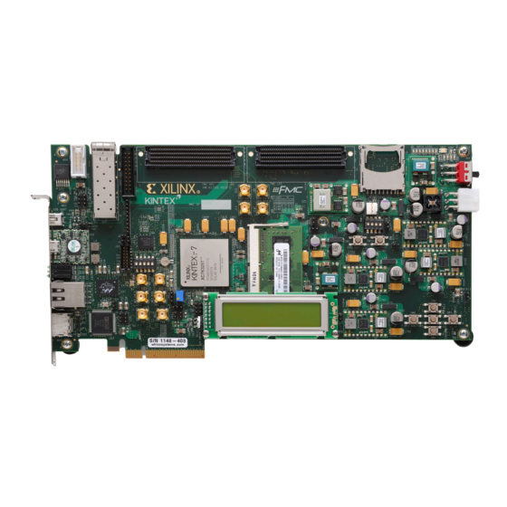
- Page 5 Xilinx KC705 Board...
- Page 6 ISE Software Requirement Xilinx ISE 14.3 software Note: Presentation applies to the KC705...
- Page 7 EDK Software Requirement Xilinx EDK 14.3 software Note: Presentation applies to the KC705...
- Page 8 EDK Software Requirement Xilinx SDK 14.3 software Note: Presentation applies to the KC705...
- Page 9 KC705 Setup Connect a USB Type-A to Micro-B cable to the USB JTAG (Digilent) connector on the KC705 board – Connect this cable to your PC – Power on the KC705 board...
- Page 10 KC705 Si5324 Setup Unzip the KC705 Si5324 Design Files (14.3 C) – Available through http://www.xilinx.com/kc705 Note: Presentation applies to the KC705...
- Page 11 Reducing Jitter with the Si5324...
- Page 12 Reducing Jitter with the Si5324 A means of measuring jitter is required for this section A LeCroy 816Zi-A Scope was used (stock photo shown) Note: Presentation applies to the KC705...
- Page 13 Reducing Jitter with the Si5324 Connect SMA cables to J13 and J14, USER_GPIO_P/N Connect these cable to your oscilloscope...
- Page 14 Reducing Jitter with the Si5324 Open ChipScope Pro and select JTAG Chain → Digilent USB Cable… Verify 30 MHz operation and click OK (2) Note: Presentation applies to the KC705...
- Page 15 Reducing Jitter with the Si5324 Click OK (1) Note: Presentation applies to the KC705...
- Page 16 Reducing Jitter with the Si5324 Select Device → DEV:0 MyDevice0 (XC7K325T) → Configure… Select <Design Path>\ready_for_download\si5324_bypass.bit Note: Presentation applies to the KC705...
- Page 17 Reducing Jitter with the Si5324 LeCroy Oscilloscope setup Press the Default Setup followed by the Auto Setup twice...
- Page 18 Reducing Jitter with the Si5324 Adjust the Horizontal knob until you have 5 μs/div...
- Page 19 Reducing Jitter with the Si5324 From the LeCroy scope menu, select Analysis → Serial Data…...
- Page 20 Reducing Jitter with the Si5324 Select “Quick View”...
- Page 21 Reducing Jitter with the Si5324 Set the inputs to Input1-Input2 and the Data to match your setup and click OK...
- Page 22 Reducing Jitter with the Si5324 Click the Close button...
- Page 23 Reducing Jitter with the Si5324 Note that the DCD (Duty Cycle Distortion) is 61.7 ps – See LeCroy presentation on Jitter for explanation of values...
- Page 24 Reducing Jitter with the Si5324 Select Device → DEV:0 MyDevice0 (XC7K325T) → Configure… – Cycle power on the KC705 to clear out any previous settings in the Si5324 Select <Design Path>\ready_for_download\si5324_enabled.bit Note: Presentation applies to the KC705...
- Page 25 Reducing Jitter with the Si5324 Note that the DCD (Duty Cycle Distortion) is 13.7 ps – Including the Si5324 Jitter Attenuator PLL in the clock path, reduces DCD...
- Page 26 Compile KC705 Si5324 Design...
- Page 27 Compile KC705 Si5324 Design If desired, FPGA compile can be skipped by opening SDK directly: Start → All Programs → Xilinx Design Tools → ISE Design Suite 14.3 → EDK → Xilinx Software Development Kit Select the workspace: <design files>\SW\SDK...
- Page 28 Compile KC705 Si5324 Design Open XPS project <project directory>\ system.xmp Create the hardware design, system.bit, located in <project directory> /implementation – Click the Generate Bitstream button (1) – Or from the menu, select Hardware → Generate Bitstream Note: Presentation applies to the KC705...
- Page 29 Launch KC705 Design in SDK Open SDK – Click the Export Design button (1) – Click Export & Launch SDK (2) Note: Presentation applies to the KC705...
- Page 30 Compile KC705 Software in SDK SDK Software Compile - Build ELF files in SDK – Select Project → Build All (1) – Note: If by-passing the FPGA compile, the ELF files are already built; if desired, the ELF files can be re-built by selecting Clean… followed by Build All...
- Page 31 Program KC705 with Si5324 Design...
- Page 32 Init memory with the Si5324 Application ELF – Update the bitstream (download.bit) with the Si5324 Application ELF – Cycle power on the KC705 to clear out any previous settings in the Si5324 – Select Xilinx Tools → Program FPGA (1)
- Page 33 Program KC705 with Si5324 Design Init memory with the Si5324 Application ELF – Select hello_iic_5324.elf (1) – Click Program Note: Presentation applies to the KC705...
- Page 34 Program KC705 with Si5324 Design Note that the DCD (Duty Cycle Distortion) has a low value now...
- Page 35 Program KC705 with Si5324 Design To set the Si5324 for Bypass mode edit the hello_iic_si5324.c Locate the line: // Change to 1 to set Si5324 into Bypass PLL mode Change the #if 0 to #if 1 Note: Presentation applies to the KC705...
- Page 36 Program KC705 with Si5324 Design To set the Si5324 for Bypass mode edit the hello_iic_si5324.c Scroll down and locate the line: // Change to 1 to set Si5324 Loop Bandwidth (BWSEL) Change the #if 1 to #if 0 Note: Presentation applies to the KC705...
- Page 37 Program KC705 with Si5324 Design Recompiled the ELF file – Select Project → Build All (1)
- Page 38 Init memory with the Si5324 Application ELF – Update the bitstream (download.bit) with the Si5324 Application ELF – Cycle power on the KC705 to clear out any previous settings in the Si5324 – Select Xilinx Tools → Program FPGA (1)
- Page 39 Program KC705 with Si5324 Design Init memory with the Si5324 Application ELF – Select hello_iic_5324.elf (1) – Click Program Note: Presentation applies to the KC705...
- Page 40 Program KC705 with Si5324 Design Note that the DCD (Duty Cycle Distortion) is now higher...
- Page 41 References...
- Page 42 References Silicon Labs – SI5324 Data Sheet • http://www.silabs.com/Support%20Documents/TechnicalDocs/Si5324.pdf LeCroy – Presentation “Jitter and Jitter Breakdown Analysis” • http://www.ist-ucells.org/news/pdf/2_jitter_and_jitter_breakdown.pdf ChipScope Pro – ChipScope Pro Software and Cores User Guide • http://www.xilinx.com/support/documentation/sw_manuals/ xilinx14_3/chipscope_pro_sw_cores_ug029.pdf...
- Page 43 Documentation...
- Page 44 Documentation Kintex-7 – Kintex-7 FPGA Family • http://www.xilinx.com/products/silicon-devices/fpga/kintex-7/index.htm KC705 Documentation – Kintex-7 FPGA KC705 Evaluation Kit • http://www.xilinx.com/products/boards-and-kits/EK-K7-KC705-G.htm – KC705 Getting Started Guide • http://www.xilinx.com/support/documentation/boards_and_kits/ ug883_K7_KC705_Eval_Kit.pdf – KC705 User Guide • http://www.xilinx.com/support/documentation/boards_and_kits/ ug810_KC705_Eval_Bd.pdf – KC705 Reference Design User Guide •...