Xilinx KC705 User Manual
Evaluation board for the kintex-7 fpga
Hide thumbs
Also See for KC705:
- User manual (118 pages) ,
- Getting started (24 pages) ,
- User manual (98 pages)
Table of Contents
Advertisement
Quick Links
Advertisement
Table of Contents

Related Manuals for Xilinx KC705


Summary of Contents for Xilinx KC705
- Page 1 KC705 Evaluation Board for the Kintex-7 FPGA User Guide UG810 (v1.3) May 10, 2013...
-
Page 2: Revision History
Limited Warranties which can be viewed at http://www.xilinx.com/warranty.htm; IP cores may be subject to warranty and support terms contained in a license issued to you by Xilinx. Xilinx products are not designed or intended to be fail-safe or for use in any application requiring fail-safe performance;... -
Page 3: Table Of Contents
KC705 Board Features ........ - Page 4 ..............90 www.xilinx.com KC705 Evaluation Board UG810 (v1.3) May 10, 2013...
-
Page 5: Chapter 1: Kc705 Evaluation Board Features
Chapter 1 KC705 Evaluation Board Features Overview The KC705 evaluation board for the Kintex™-7 FPGA provides a hardware environment for developing and evaluating designs targeting the Kintex-7 XC7K325T-2FFG900C FPGA. The KC705 board provides features common to many embedded processing systems, including a DDR3 SODIMM memory, an 8-lane PCI Express®... - Page 6 Chapter 1: KC705 Evaluation Board Features • Ethernet PHY SGMII interface (RJ-45 connector) • PCI Express endpoint connectivity • Gen1 8-lane (x8) • Gen2 8-lane (x8) • SFP+ Connector • 10/100/1000 tri-speed Ethernet PHY • USB-to-UART bridge • HDMI codec •...
-
Page 7: Feature Descriptions
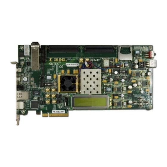
The KC705 Evaluation Kit Product Page: www.xilinx.com/kc705 Caution! The KC705 board can be damaged by electrostatic discharge (ESD). Follow standard ESD prevention measures when handling the board X-Ref Target - Figure 1-1 1 GB DDR3 Memory... - Page 8 Chapter 1: KC705 Evaluation Board Features X-Ref Target - Figure 1-2 Round callout references a component Square callout references a component on the front side of the board on the back side of the board User rotary switch located under LCD...
-
Page 9: Kintex-7 Fpga
For further information on Kintex-7 FPGAs, see DS180 , 7 Series FPGAs Overview FPGA Configuration The KC705 board supports three of the five 7 Series FPGA configuration modes: • Master SPI using the onboard Quad SPI Flash memory • Master BPI using the on-board Linear BPI Flash memory •... - Page 10 For full details on configuring the FPGA, see UG470, 7 Series FPGAs Configuration User Guide Encryption Key Backup Circuit FPGA U1 implements bitstream encryption key technology. The KC705 board provides the encryption key backup battery circuit shown in Figure 1-4. The rechargeable 1.5V lithium button-type battery B1 is soldered to the board with the positive output connected to FPGA U1 VCCBATT pin C10.
- Page 11 Figure 1-4: Encryption Key Backup Circuit I/O Voltage Rails There are 10 I/O banks available on the Kintex-7 device. The voltages applied to the FPGA I/O banks used by the KC705 board are listed in Table 1-3. Table 1-3: I/O Voltage Rails...
-
Page 12: Ddr3 Memory Module
Chapter 1: KC705 Evaluation Board Features DDR3 Memory Module [Figure 1-2, callout 2] The memory module at J1 is a 1 GB DDR3 small outline dual-inline memory module (SODIMM). It provides volatile synchronous dynamic random access memory (SDRAM) for storing user code and data. - Page 13 DDR3_D22 DQ22 AD19 DDR3_D23 DQ23 AK16 DDR3_D24 DQ24 AJ17 DDR3_D25 DQ25 AG15 DDR3_D26 DQ26 AF15 DDR3_D27 DQ27 AH17 DDR3_D28 DQ28 AG14 DDR3_D29 DQ29 AH15 DDR3_D30 DQ30 AK15 DDR3_D31 DQ31 DDR3_D32 DQ32 KC705 Evaluation Board www.xilinx.com UG810 (v1.3) May 10, 2013...
- Page 14 Chapter 1: KC705 Evaluation Board Features Table 1-4: DDR3 Memory Connections to the FPGA (Cont’d) J1 DDR3 Memory U1 FPGA Pin Net Name Pin Number Pin Name DDR3_D33 DQ33 DDR3_D34 DQ34 DDR3_D35 DQ35 DDR3_D36 DQ36 DDR3_D37 DQ37 DDR3_D38 DQ38 DDR3_D39...
- Page 15 DDR3_DQS5_P DQS5_P DDR3_DQS6_N DQS6_N DDR3_DQS6_P DQS6_P DDR3_DQS7_N DQS7_N DDR3_DQS7_P DQS7_P DDR3_ODT0 ODT0 AC10 DDR3_ODT1 ODT1 DDR3_RESET_B RESET_B AC12 DDR3_S0_B S0_B DDR3_S1_B S1_B DDR3_TEMP_EVENT EVENT_B DDR3_WE_B WE_B AC11 DDR3_CAS_B CAS_B DDR3_RAS_B RAS_B KC705 Evaluation Board www.xilinx.com UG810 (v1.3) May 10, 2013...
-
Page 16: Linear Bpi Flash Memory
AE11 DDR3_CLK1_P CK1_P The KC705 DDR3 SODIMM interface adheres to the constraints guidelines documented in the DDR3 Design Guidelines section of UG586, 7 Series FPGAs Memory Interface Solutions User Guide. The KC705 DDR3 SODIMM interface is a 40Ω impedance implementation. - Page 17 FLASH_A1 FLASH_A2 FLASH_A3 FLASH_A4 FLASH_A5 FLASH_A6 FLASH_A7 FLASH_A8 FLASH_A9 FLASH_A10 FLASH_A11 FLASH_A12 FLASH_A13 FLASH_A14 FLASH_A15 FLASH_A16 FLASH_A17 FLASH_A18 FLASH_A19 FLASH_A20 FLASH_A21 FLASH_A22 FLASH_A23 FLASH_A24 FLASH_A25 FLASH_D0 FLASH_D1 FLASH_D2 FLASH_D3 FLASH_D4 FLASH_D5 KC705 Evaluation Board www.xilinx.com UG810 (v1.3) May 10, 2013...
- Page 18 Configuration User Guide. The configuration section in this document provides details on the Master BPI configuration mode. Figure 1-5 shows the connections of the linear BPI Flash memory on the KC705 board. For more information about the Numonyx PC28F00AP30TF see [Ref www.xilinx.com...
-
Page 19: Quad-Spi Flash Memory
• Part number: N25Q128A13BSF40F (Numonyx) • Supply voltage: 2.8V • Datapath width: 4 bits • Data rate: Various depending on Single/Dual/Quad mode and CCLK rate KC705 Evaluation Board www.xilinx.com UG810 (v1.3) May 10, 2013... -
Page 20: Sd Card Interface
The configuration section of UG470, 7 Series FPGAs Configuration User Guide provides details on using the Quad-SPI Flash memory. Figure 1-6 shows the connections of the Quad-SPI Flash memory on the KC705 board. For more information about the Numonyx N25Q128A13BSF40F see [Ref X-Ref Target - Figure 1-6... - Page 21 Feature Descriptions The KC705 board includes a secure digital input/output (SDIO) interface to provide user-logic access to general purpose non-volatile SDIO memory cards and peripherals. The SD card slot is designed to support 50 MHz high speed SD cards. The SDIO signals are connected to I/O bank 12 which has its VCCO set to VADJ. A Texas Instruments I TXB0108 8-bit bidirectional voltage-level translator is used between the FPGA and the SD card connector (U9).
-
Page 22: Usb Jtag Module
UG810_c1_07_120211 Figure 1-8: JTAG Chain Block Diagram When an FMC mezzanine card is attached to the KC705 board it is automatically added to the JTAG chain through electronically controlled single-pole single-throw (SPST) switches U76 and U77. The SPST switches are in a normally closed state and transition to an open state when an FMC mezzanine card is attached. -
Page 23: Clock Generation
Translator FPGA_TMS_BUF FPGA_TCK_BUF FPGA_TDO UG810_c1_08_012012 Figure 1-9: JTAG Circuit Clock Generation There are five clock sources available for the FPGA fabric on the KC705 board (refer to Table 1-8). Table 1-8: KC705 Board Clock Sources Clock Name Reference Description System Clock SiT9102 2.5V LVDS 200 MHz Fixed Frequency... - Page 24 [Figure 1-2, callout 7] The KC705 board has a 2.5V LVDS differential 200 MHz oscillator (U6) soldered onto the back side of the board and wired to an FPGA MRCC clock input on bank 33. This 200 MHz signal pair is named SYSCLK_P and SYSCLK_N, which are connected to FPGA U1 pins AD12 and AD11 respectively.
- Page 25 10 MHz to 810 MHz through an I C interface. Power cycling the KC705 board will revert the user clock to its default frequency of 156.250 MHz. • Programmable Oscillator: Silicon Labs Si570BAB0000544DG (10 MHz - 810 MHz) •...
- Page 26 Chapter 1: KC705 Evaluation Board Features Reference design files are available to demonstrate how to program the Si570 programmable oscillator. See: • XTP186, KC705 Si570 Programming • RDF0175, Reference Design Files • XTP187, KC705 Si570 Fixed Frequencies • RDF0176, Reference Design Files www.xilinx.com...
- Page 27 [Figure 1-2, callout 10] The KC705 board includes a pair of SMA connectors for a GTX clock wired to GTX Quad bank 117. This differential clock has signal names SMA_MGT_REFCLK_P and SMA_REFCLK_N, which are connected to FPGA U1 pins J8 and J7 respectively.
- Page 28 [Figure 1-2, callout 11] The KC705 board includes a Silicon Labs Si5324 jitter attenuator U70 on the back side of the board. FPGA user logic can implement a clock recovery circuit and then output this clock to a differential I/O pair on I/O bank 13 (REC_CLOCK_C_P, FPGA U1 pin W27 and REC_CLOCK_C_N, FPGA U1 pin W28) for jitter attenuation.
-
Page 29: Gtx Transceivers
The GTX transceivers in 7 Series FPGAs are grouped into four channels described as Quads. The reference clock for a Quad can be sourced from the Quad above or Quad below the GTX Quad of interest. There are four GTX Quads on the KC705 board with connectivity as shown here: •... -
Page 30: Pci Express Edge Connector
100Ω differential pair. The 7 series FPGAs GTX transceivers are used for multi-gigabit per second serial interfaces. The XC7K325T-2FFG900C FPGA (-2 speed grade) included with the KC705 board supports up to Gen2 x8. The PCIe clock is input from the edge connector. It is AC coupled to the FPGA through the MGTREFCLK1 pins of Quad 115. - Page 31 PETp7 Integrated Endpoint block receive pair GTXE2_CHANNEL_X0Y0 PCIE_RX7_N PETn7 Integrated Endpoint block receive pair GTXE2_CHANNEL_X0Y0 PCIE_TX0_P PERp0 Integrated Endpoint block transmit pair GTXE2_CHANNEL_X0Y7 PCIE_TX0_N PERn0 Integrated Endpoint block transmit pair GTXE2_CHANNEL_X0Y7 KC705 Evaluation Board www.xilinx.com UG810 (v1.3) May 10, 2013...
- Page 32 Chapter 1: KC705 Evaluation Board Features Table 1-11: PCIe Edge Connector Connections (Cont’d) Schematic FPGA Pin PCIe Edge PCIe Edge Pin FFG900 Function Net Name (U1) Connector Pin Name Placement PCIE_TX1_P PERp1 Integrated Endpoint block transmit pair GTXE2_CHANNEL_X0Y6 PCIE_TX1_N PERn1...
- Page 33 GTXE2_CHANNEL_X0Y6 MGTXRXP2_116_P6 PCIE_RX1_P PETp1 GTXE2_CHANNEL_X0Y6 MGTXRXN2_116_P5 PCIE_RX1_N PETn1 GTXE2_CHANNEL_X0Y6 MGTXTXP3_116_L4 PCIE_TX0_P PERp0 GTXE2_CHANNEL_X0Y7 MGTXTXN3_116_L3 PCIE_TX0_N PERn0 GTXE2_CHANNEL_X0Y7 MGTXRXP3_116_M6 PCIE_RX0_P PETp0 GTXE2_CHANNEL_X0Y7 MGTXRXN3_116_M5 PCIE_RX0_N PETn0 GTXE2_CHANNEL_X0Y7 MGTREFCLK0P_116_L8 SI5326_OUT_C_P MGT_BANK_116 MGTREFCLK0N_116_L7 SI5326_OUT_C_N MGT_BANK_116 KC705 Evaluation Board www.xilinx.com UG810 (v1.3) May 10, 2013...
-
Page 34: Sfp/Sfp+ Connector
7 Series FPGAs Integrated Block for PCI Express User Guide (AXI). SFP/SFP+ Connector [Figure 1-2, callout 14] The KC705 board contains a small form-factor pluggable (SFP+) connector and cage assembly that accepts SFP or SFP+ modules. Figure 1-17 shows the SFP+ module connector circuitry. - Page 35 SFP+ module RX and TX connections to the FPGA. Table 1-14: FPGA U1 to SFP+ Module Connections FPGA Pin Schematic SFP+ Pin SFP+ Pin Name (U1) Net Name (P5) (P5) SFP_RX_N RD_N SFP_RX_P RD_P SFP_TX_N TX_N SFP_TX_P TX_P KC705 Evaluation Board www.xilinx.com UG810 (v1.3) May 10, 2013...
-
Page 36: 10/100/1000 Tri-Speed Ethernet Phy
SFP_TX_DISABLE_TRANS TX_DISABLE Notes: 1. On KC705 boards prior to Rev 1.1, SFP+ connector P5 pin 18 TD_P is connected to net SFP_TX_N, and pin 19 TD_N is connected to net SFP_TX_P. Table 1-15 lists the SFP+ module control and status connections to the FPGA. - Page 37 GTX transceiver (clock pins G8 (P) and G7 (N)) driving the SGMII interface. Series AC coupling capacitors are present to allow the clock input of the FPGA to set the common mode voltage. Figure 1-18 shows the Ethernet SGMII clock source. KC705 Evaluation Board www.xilinx.com UG810 (v1.3) May 10, 2013...
- Page 38 Chapter 1: KC705 Evaluation Board Features X-Ref Target - Figure 1-18 VDDA_SGMIICLK VDD_SGMIICLK 18pF 50V ICS844021I-01 Clock Generator 25.00 MHz 0.1μF 25V VDDA SGMIICLK_XTAL_OUT SGMIICLK_Q0_C_P SGMIICLK_Q0_P R134 GND2 XTAL_OUT 1.0MΩ 5% GND2 SGMIICLK_XTAL_IN SGMIICLK_Q0_C_N SGMIICLK_Q0_N XTAL_IN 18pF 50V 0.1μF 25V...
-
Page 39: Usb-To-Uart Bridge
USB cable is plugged into the USB port on the KC705 board. Xilinx UART IP is expected to be implemented in the FPGA fabric. The FPGA supports the USB-to-UART bridge using four signal pins: Transmit (TX), Receive (RX), Request to Send (RTS), and Clear to Send (CTS). -
Page 40: Hdmi Video Output
[Figure 1-2, callout 18] The KC705 board provides a High-Definition Multimedia Interface (HDMI) video output using the Analog Devices ADV7511KSTZ-P HDMI transmitter (U65). The HDMI output is provided on a Molex 500254-1927 HDMI type-A connector (P6). The ADV7511 is wired to support 1080P 60Hz, YCbCr 4:2:2 encoding via 16-bit input data mapping. - Page 41 HDMI_CEC DSD3 DSD4 DSD5 DSD_CLK MCLK GND1 GND2 GND3 I2S0 GND4 I2S1 GND5 I2S2 GND6 I2S3 GND7 SCLK GND8 LRCLK GND9 GND10 R_EXT GND11 R433 UG810_c1_18_011912 Figure 1-19: HDMI Codec Circuit KC705 Evaluation Board www.xilinx.com UG810 (v1.3) May 10, 2013...
- Page 42 Chapter 1: KC705 Evaluation Board Features Table 1-21 lists the connections between the codec and the FPGA. Table 1-21: FPGA to HDMI Codec Connections (ADV7511) ADV7511 (U65) FPGA Pin Schematic Net Name (U1) Pin Number Pin Name HDMI_D0 HDMI_D1 HDMI_D2...
-
Page 43: Lcd Character Display
HDMI_CRC For more information about the ADV7511KSTZ-P see [Ref LCD Character Display [Figure 1-2, callout 19] A 2-line by 16-character display is provided on the KC705 board (Figure 1-20). X-Ref Target - Figure 1-20 LCD Display (16 x 2) UG810_c1_19_121211 Figure 1-20: LCD Display The character display runs at 5.0V and is connected to the FPGA's 1.5V HP bank 33... - Page 44 UG810_c1_20_121211 Figure 1-21: LCD Interface Circuit The KC705 board base board uses a male Samtec MTLW-107-07-G-D-265 2x7 header (J31) with 0.025-inch square posts on 0.100-inch centers for connecting to a Samtec SLW-107-01-L-D female socket on the LCD display panel assembly. The LCD header...
-
Page 45: I2C Bus Switch
For more information about the Displaytech S162D LCD see [Ref I2C Bus Switch [Figure 1-2, callout 20] The KC705 board implements a single I C port on the FPGA (IIC_SDA_MAIN, IIC_SDA_SCL), which is routed through a TI PCA9548 1-to-8 channel I C switch (U49). The I C switch can operate at speeds up to 400 kHz. -
Page 46: Status Leds
Chapter 1: KC705 Evaluation Board Features Table 1-24 lists the address for each bus. Table 1-24: I C Buses C Switch C Bus C Address Position USER_CLOCK_SDA/SCL 0b1011101 FMC_HPC_IIC_SDA/SCL 0bXXXXX00 FMC_LPC_IIC_SDA/SCL 0bXXXXX00 EEPROM_IIC_SDA/SCL 0b1010100 SFP_IIC_SDA/SCL 0b1010000 IIC_SDA/SCL_HDMI 0b0111001 IIC_SDA/SCL_DDR3 0b1010000, 0b0011000... -
Page 47: Ethernet Phy Status Leds
The Ethernet PHY status LEDs are mounted to be visible through the metal bracket on the left edge of the KC705 board when it is installed into a PCIe slot in a PC chassis. The six PHY status LEDs are located above the RJ45 Ethernet jack as shown in Figure 1-24. - Page 48 Chapter 1: KC705 Evaluation Board Features • User Rotary Switch (callout 25, hidden beneath the LCD) • ROTARY_PUSH, ROTARY_INCA, ROTARY_INCB: SW8 • User SMA (callout 26) • USER_SMA_GPIO_P, USER_SMA_GPIO_N: J13, J14 • 2 line x 16 character LCD Character Display (callout 19) •...
- Page 49 CPU Reset Pushbutton [Figure 1-2, callout 37] Figure 1-27 shows the CPU reset pushbutton circuit. X-Ref Target - Figure 1-27 VCC1V5 CPU_RESET 4.7kΩ 0.1 W UG810_c1_11_042313 Figure 1-27: CPU Reset Pushbutton KC705 Evaluation Board www.xilinx.com UG810 (v1.3) May 10, 2013...
- Page 50 Chapter 1: KC705 Evaluation Board Features GPIO DIP Switch [Figure 1-2, callout 24] Figure 1-28 shows the GPIO DIP Switch circuit. X-Ref Target - Figure 1-28 SW11 VADJ GPIO_DIP_SW3 GPIO_DIP_SW2 GPIO_DIP_SW1 GPIO_DIP_SW0 SDA04H1SBD 4.7kΩ 4.7kΩ 0.1 W 0.1 W 4.7kΩ...
- Page 51 Indicator LEDs (Active High) GPIO_LED_0 DS4.2 GPIO_LED_1 DS1.2 GPIO_LED_2 DS10.2 GPIO_LED_3 DS2.2 AE26 GPIO_LED_4 DS3.2 GPIO_LED_5 DS25.2 GPIO_LED_6 DS26.2 GPIO_LED_7 DS27.2 Directional Push-Button Switches AA12 GPIO_SW_N SW2.1 GPIO_SW_E SW3.1 AB12 GPIO_SW_S SW4.1 KC705 Evaluation Board www.xilinx.com UG810 (v1.3) May 10, 2013...
-
Page 52: Switches
[Figure 1-2, callout 27] The KC705 board power switch is SW15. Sliding the switch actuator from the Off to On position applies 12V power from J49, a 6-pin mini-fit connector. Green LED DS22 illuminates when the KC705 board power is on. See... - Page 53 The KC705 Evaluation Kit provides the adapter cable shown in Figure 1-32 for powering the KC705 board from the ATX power supply 4-pin peripheral connector. The Xilinx part number for this cable is 2600304, and is equivalent to Sourcegate Technologies part number AZCBL-WH-1109-RA4.
-
Page 54: Fpga Mezzanine Card Interface
1-2, callout - 31] The KC705 board supports the VITA 57.1 FPGA Mezzanine Card (FMC) specification by providing subset implementations of a high pin count (HPC) connector at J22 and a low pin count (LPC) connector at J2. Both connectors use the same 10 x 40 form factor, except the HPC version is fully populated with 400 pins and the LPC version is partially populated with 160 pins. - Page 55 The HPC signals are distributed across GTX Quads 116, 117, and 118. Each of these Quads have their VCCO voltage connected to VADJ. Note: The KC705 board VADJ voltage for the J22 and J2 connectors is determined by the FMC VADJ power sequencing logic described in the Power Management, page...
- Page 56 Chapter 1: KC705 Evaluation Board Features Table 1-28: HPC Connections, J22 to FPGA U1 (Cont’d) FPGA U1 FPGA U1 J22 Pin Net Name J22 Pin Net Name FMC_HPC_DP1_C2M_P FMC_HPC_GBTCLK1_M2C_N FMC_HPC_DP1_C2M_N FMC_HPC_DP2_C2M_P FMC_HPC_DP2_C2M_N FMC_HPC_DP3_C2M_P FMC_HPC_DP3_C2M_N FMC_HPC_DP0_C2M_P PWRCTL1_VCC4A_PG FMC_HPC_DP0_C2M_N FMC_HPC_GBTCLK0_M2C_P FMC_HPC_DP0_M2C_P FMC_HPC_GBTCLK0_M2C_N...
- Page 57 VCC3V3 VCC3V3 VCC3V3 FMC_HPC_HA01_CC_P FMC_HPC_PG_M2C FMC_HPC_HA01_CC_N FMC_HPC_HA00_CC_P FMC_HPC_HA05_P FMC_HPC_HA00_CC_N FMC_HPC_HA05_N FMC_HPC_HA04_P FMC_HPC_HA09_P FMC_HPC_HA04_N FMC_HPC_HA09_N FMC_HPC_HA08_P FMC_HPC_HA13_P FMC_HPC_HA08_N FMC_HPC_HA13_N FMC_HPC_HA12_P FMC_HPC_HA16_P FMC_HPC_HA12_N FMC_HPC_HA16_N FMC_HPC_HA15_P FMC_HPC_HA20_P FMC_HPC_HA15_N FMC_HPC_HA20_N FMC_HPC_HA19_P FMC_HPC_HA19_N VADJ VADJ FMC_HPC_CLK1_M2C_P KC705 Evaluation Board www.xilinx.com UG810 (v1.3) May 10, 2013...
- Page 58 Chapter 1: KC705 Evaluation Board Features Table 1-28: HPC Connections, J22 to FPGA U1 (Cont’d) FPGA U1 FPGA U1 J22 Pin Net Name J22 Pin Net Name FMC_HPC_CLK1_M2C_N FMC_HPC_PRSNT_M2C_B FMC_HPC_LA00_CC_P FMC_HPC_CLK0_M2C_P FMC_HPC_LA00_CC_N FMC_HPC_CLK0_M2C_N FMC_HPC_LA03_P FMC_HPC_LA02_P FMC_HPC_LA03_N FMC_HPC_LA02_N FMC_HPC_LA08_P FMC_HPC_LA04_P FMC_HPC_LA08_N...
- Page 59 61 ground and 10 power connections The connections between the LPC connector at J2 and FPGA U1 (Table 1-29) implement a subset of this connectivity: • 34 differential user defined pairs • 34 LA pairs (LA00-LA33) KC705 Evaluation Board www.xilinx.com UG810 (v1.3) May 10, 2013...
- Page 60 Chapter 1: KC705 Evaluation Board Features • 1 GTX transceiver • 1 GTX clock • 2 differential clocks • 61 ground and 9 power connections Table 1-29: LPC Connections, J2 to FPGA U1 FPGA U1 FPGA U1 J2 Pin Net Name...
-
Page 61: Power Management
[Figure 1-2, callout 32] The KC705 board uses power regulators and PMBus compliant digital PWM system controllers from Texas Instruments to supply core and auxiliary voltages. The Texas Instruments Fusion Digital Power graphical user interface is used to monitor the current and temperature levels of the board's power modules. - Page 62 The PCB layout and power system have been designed to meet the recommended criteria described in UG483, 7 Series FPGAs PCB Design and Pin Planning Guide. The KC705 board power distribution diagram is shown in Figure 1-35. X-Ref Target - Figure 1-35...
- Page 63 Feature Descriptions The KC705 board core and auxiliary voltages are listed in Table 1-30. Table 1-30: Onboard Power System Devices Reference Power Rail Power Rail Schematic Device Type Description Designator Net Name Voltage Page Core voltage controller and regulators UCD9248PFC...
- Page 64 Chapter 1: KC705 Evaluation Board Features FMC_VADJ Voltage Control The FMC_VADJ rail is set to 2.5V. When the KC705 board is powered on, the state of the FMC_VADJ_ON_B signal wired to header J65 is sampled by the Texas Instruments UCD9248 controller U55. If a jumper is installed on J65, signal FMC_VADJ_ON_B is held low, and the TI controller U55 energizes the FMC_VADJ rail at power on.
- Page 65 Table 1-32: Power Rail Specifications for UCD9248 PMBus controller at Address 53 Shutdown Threshold Rail Rail Schematic Number Name Rail Name Rail #1 VCC2V5_FPGA 2.25 2.125 2.875 10.41 Rail #2 VCC1V5 1.35 1.275 1.725 10.41 KC705 Evaluation Board www.xilinx.com UG810 (v1.3) May 10, 2013...
-
Page 66: Xadc Header
Chapter 1: KC705 Evaluation Board Features Table 1-32: Power Rail Specifications for UCD9248 PMBus controller at Address 53 (Cont’d) Shutdown Threshold Rail Rail Schematic Number Name Rail Name Rail #3 MGTAVCC 0.85 1.45 10.41 Rail #4 MGTAVTT 1.08 1.02 1.38 10.41... - Page 67 UG810_c1_30_042313 Figure 1-37: Header XADC_VREF Voltage Source Options The KC705 board supports both the internal FPGA sensor measurements and the external measurement capabilities of the XADC. Internal measurements of the die temperature, VCCINT, VCCAUX, and VCCBRAM are available. The KC705 board VCCINT and VCCBRAM are provided by a common 1.0 V supply.
- Page 68 Chapter 1: KC705 Evaluation Board Features X-Ref Target - Figure 1-38 XADC_VN XADC_VP XADC_VAUX0P XADC_VAUX0N XADC_VCC5V0 XADC_VAUX8P XADC_VAUX8N XADC_DXP VADJ XADC_VREF XADC_DXN XADC_VCC_HEADER XADC_GPIO_1 XADC_GPIO_0 XADC_GPIO_2 XADC_GPIO_3 XADC_AGND XADC_AGND UG810_c1_31_121311 Figure 1-38: XADC header (J46) Table 1-34 describes the XADC header J46 pin functions.
-
Page 69: Configuration Options
Configuration Options Configuration Options The FPGA on the KC705 board can be configured by the following methods: • Master BPI (uses the Linear BPI Flash). • Master SPI (uses the Quad-SPI Flash). • JTAG (uses the USB-to-JTAG Bridge or Download cable). See... - Page 70 Chapter 1: KC705 Evaluation Board Features FPGA over the 16-bit data path from the Linear BPI Flash memory at a maximum synchronous read rate of 33 MHz. The bitstream stored in the Flash memory must be generated with a bitgen option to divide the EMCCLK by two.
-
Page 71: Appendix A: Default Switch And Jumper Settings
Figure A-2 and details are listed in Table A-2. X-Ref Target - Figure A-2 ON Position = 1 2 3 4 5 OFF Position = 0 UG810_aB_02_010512 Figure A-2: SW13 Default Settings KC705 Evaluation Board www.xilinx.com UG810 (v1.3) May 10, 2013... -
Page 72: Default Jumper Settings
Pin 1 to pin 2 Pin 1 to pin 2 None Pin 1 to pin 2 Pin 2 to pin 3 None None Pin 1 to pin 2 Pin 1 to pin 2 www.xilinx.com KC705 Evaluation Board UG810 (v1.3) May 10, 2013... -
Page 73: Appendix B: Vita 57.1 Fmc Connector Pinouts
Figure B-1 shows the pinout of the FPGA mezzanine card (FMC) high pin count (HPC) connector defined by the VITA 57.1 FMC specification. For a description of how the KC705 board implements the FMC specification, see FPGA Mezzanine Card Interface, page 54... - Page 74 Figure B-2 shows the pinout of the FPGA mezzanine card (FMC) ligh pin count (LPC) connector defined by the VITA 57.1 FMC specification. For a description of how the KC705 board implements the FMC specification, see FPGA Mezzanine Card Interface, page 54...
-
Page 75: Appendix C: Master Ucf Listing
The KC705 board master user constraints file (UCF) template provides for designs targeting the KC705 board. Net names in the constraints listed below correlate with net names on the latest KC705 board schematic. Users must identify the appropriate pins and replace the net names below with net names in the user RTL. - Page 76 14 VCCO - VCC2V5_FPGA - IO_L7P_T1_D09_14 FLASH_D10 LOC = R29 | IOSTANDARD=LVCMOS25; # Bank 14 VCCO - VCC2V5_FPGA - IO_L7N_T1_D10_14 FLASH_D11 LOC = P27 | IOSTANDARD=LVCMOS25; # Bank 14 VCCO - VCC2V5_FPGA - IO_L8P_T1_D11_14 www.xilinx.com KC705 Evaluation Board UG810 (v1.3) May 10, 2013...
- Page 77 KC705 Board UCF Listing FLASH_D12 LOC = P28 | IOSTANDARD=LVCMOS25; # Bank 14 VCCO - VCC2V5_FPGA - IO_L8N_T1_D12_14 PHY_CRS LOC = R30 | IOSTANDARD=LVCMOS25; # Bank 14 VCCO - VCC2V5_FPGA - IO_L9P_T1_DQS_14 FLASH_D13 LOC = T30 | IOSTANDARD=LVCMOS25; # Bank...
- Page 78 17 VCCO - VADJ_FPGA - IO_L13P_T2_MRCC_17 FMC_HPC_CLK1_M2C_N LOC = D18 | IOSTANDARD=LVCMOS25; # Bank 17 VCCO - VADJ_FPGA - IO_L13N_T2_MRCC_17 FMC_HPC_LA20_P LOC = E19 | IOSTANDARD=LVCMOS25; # Bank 17 VCCO - VADJ_FPGA - IO_L14P_T2_SRCC_17 www.xilinx.com KC705 Evaluation Board UG810 (v1.3) May 10, 2013...
- Page 79 KC705 Board UCF Listing FMC_HPC_LA20_N LOC = D19 | IOSTANDARD=LVCMOS25; # Bank 17 VCCO - VADJ_FPGA - IO_L14N_T2_SRCC_17 FMC_HPC_LA28_P LOC = D16 | IOSTANDARD=LVCMOS25; # Bank 17 VCCO - VADJ_FPGA - IO_L15P_T2_DQS_17 FMC_HPC_LA28_N LOC = C16 | IOSTANDARD=LVCMOS25; # Bank...
- Page 80 33 VCCO - VCC1V5_FPGA - IO_L20N_T3_33 DDR3_A7 LOC = AH14 | IOSTANDARD=SSTL15; # Bank 33 VCCO - VCC1V5_FPGA - IO_L21P_T3_DQS_33 DDR3_A6 LOC = AJ14 | IOSTANDARD=SSTL15; # Bank 33 VCCO - VCC1V5_FPGA - IO_L21N_T3_DQS_33 www.xilinx.com KC705 Evaluation Board UG810 (v1.3) May 10, 2013...
- Page 81 KC705 Board UCF Listing DDR3_A5 LOC = AJ13 | IOSTANDARD=SSTL15; # Bank 33 VCCO - VCC1V5_FPGA - IO_L22P_T3_33 DDR3_A4 LOC = AJ12 | IOSTANDARD=SSTL15; # Bank 33 VCCO - VCC1V5_FPGA - IO_L22N_T3_33 DDR3_A3 LOC = AF12 | IOSTANDARD=SSTL15; # Bank...
- Page 82 - MGTXTXP0_118 FMC_HPC_DP0_M2C_P LOC = E4 ; # Bank 118 - MGTXRXP0_118 FMC_HPC_DP0_C2M_N LOC = D1 ; # Bank 118 - MGTXTXN0_118 FMC_HPC_DP0_M2C_N LOC = E3 ; # Bank 118 - MGTXRXN0_118 www.xilinx.com KC705 Evaluation Board UG810 (v1.3) May 10, 2013...
-
Page 83: Appendix D: Board Setup
Figure D-1: Plug the 6-pin 2 x 3 Molex connector on the adapter cable into J49 on the KC705 board. b. Plug the 4-pin 1 x 4 peripheral power connector from the ATX power supply into the 4-pin adapter cable connector. - Page 84 Appendix D: Board Setup Slide the KC705 board power switch SW12 to the ON position. The PC can now be powered on. www.xilinx.com KC705 Evaluation Board UG810 (v1.3) May 10, 2013...
-
Page 85: Appendix E: Board Specifications
Board Specifications Dimensions Height 5.5 in (14.0 cm) Length 10.5 in (26.7 cm) Note: The KC705 board height exceeds the standard 4.376 in (11.15 cm) height of a PCI Express card. Environmental Temperature Operating: 0°C to +45°C Storage: –25°C to +60°C... - Page 86 Appendix E: Board Specifications www.xilinx.com KC705 Evaluation Board UG810 (v1.3) May 10, 2013...
-
Page 87: Appendix F: Additional Resources
Topics include design assistance, advisories, and troubleshooting tips. Further Resources The most up to date information related to the KC705 board and its documentation is available on the following websites. The KC705 Evaluation Kit Product Page: www.xilinx.com/kc705... -
Page 88: References
UG476, 7 Series FPGAs GTX Transceivers User Guide PG054 7 Series FPGAs Integrated Block for PCI Express User Guide XTP186, KC705 Si570 Programming XTP187, KC705 Si570 Fixed Frequencies UG625, Constraints Guide References The following websites provide supplemental material useful with this guide: Analog Devices: http://www.analog.com/en/index.html... -
Page 89: Appendix G: Regulatory And Compliance Information
EN 55024:2010, Information Technology Equipment Immunity Characteristics – Limits and Methods of Measurement This is a Class A product and can cause radio interference. In a domestic environment, the user might be required to take adequate corrective measures. KC705 Evaluation Board www.xilinx.com UG810 (v1.3) May 10, 2013... -
Page 90: Safety
This product complies with Directive 2002/95/EC on the restriction of hazardous substances (RoHS) in electrical and electronic equipment. This product complies with CE Directives 2006/95/EC, Low Voltage Directive (LVD) and 2004/108/EC, Electromagnetic Compatibility (EMC) Directive. www.xilinx.com KC705 Evaluation Board UG810 (v1.3) May 10, 2013...