Xilinx KCU105 User Manual
Hide thumbs
Also See for KCU105:
- User manual (110 pages) ,
- Software install and board setup (32 pages) ,
- Quick start manual (4 pages)
Table of Contents
Advertisement
Advertisement
Table of Contents

Related Manuals for Xilinx KCU105


Summary of Contents for Xilinx KCU105
- Page 1 KCU105 Board User Guide UG917 (v1.4) September 25, 2015...
-
Page 2: Revision History
Controller. Updated Clock Menu section. Updated the KCU105 Board Constraints File Listing in Appendix D. Updated the KCU105 evaluation kit master answer record number. 12/18/2014 Initial Xilinx release. KCU105 Board User Guide www.xilinx.com Send Feedback UG917 (v1.4) September 25, 2015... -
Page 3: Table Of Contents
KCU105 Board Zynq-7000 AP SoC XC7Z010 System Controller ....... . . - Page 4 Installing the KCU105 Board in a PC Chassis ....... . .
- Page 5 Xilinx Resources ........
-
Page 6: Chapter 1: Kcu105 Evaluation Board Features
Other features can be added by using VITA-57 FPGA mezzanine cards (FMCs) attached to the low pin count (LPC) FMC and high pin count (HPC) FMC connectors. KCU105 Evaluation Board Features The KCU105 evaluation board features are listed here. Detailed information for each feature is provided in Feature Descriptions. - Page 7 Chapter 1: KCU105 Evaluation Board Features FMC LPC connector (one GTH transceiver) ° 8-Lane PCI Express (eight GTH transceivers) ° Two SFP+ connectors (two GTH transceivers) ° TX and RX pair SMA connectors (one GTH transceiver) ° • PCI Express endpoint connectivity Gen1 8-lane (x8) °...
-
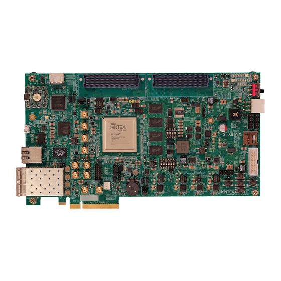
Page 8: Board Diagram
Chapter 1: KCU105 Evaluation Board Features Board Diagram The KCU105 board diagram is shown in Figure 1-1 X-Ref Target - Figure 1-1 Figure 1-1: KCU105 Evaluation Board Block Diagram KCU105 Board User Guide www.xilinx.com Send Feedback UG917 (v1.4) September 25, 2015... -
Page 9: Feature Descriptions
IMPORTANT: board. The KCU105 board can be damaged by electrostatic discharge (ESD). Follow standard ESD CAUTION! prevention measures when handling the board. X-Ref Target - Figure 1-2... - Page 10 Chapter 1: KCU105 Evaluation Board Features Table 1-1: KCU105 Board Component Descriptions Schematic Callout Component Description Notes 0381556 Page Number Kintex UltraScale XCKU040-2FFVA1156E Device XCKU040-2FFVA1156E With fan-sink on top of the FPGA soldered on Radian FB95+K52B+T710 the board DDR4 Component...
- Page 11 Chapter 1: KCU105 Evaluation Board Features Table 1-1: KCU105 Board Component Descriptions (Cont’d) Schematic Callout Component Description Notes 0381556 Page Number Dual USB-to-UART Bridge, Silicon Labs CP2105-F01-GM bridge, Bridge device (U34) with Mini-B Connector (J4) Hirose ZX62D-AB-5P8 connector HDMI Video...
-
Page 12: Kintex Ultrascale Xcku040-2Ffva1156E Device
On/Off Slide Switch SW1 Rotary Switch, PANASONIC EVQ-WK4001 Active-High (SW13) Notes: 1. The KCU105 board schematics are available for download. See the KCU105 Evaluation Kit website. 2. The KCU105 board jumper header locations are shown in Figure A-1. Kintex UltraScale XCKU040-2FFVA1156E Device... - Page 13 Chapter 1: KCU105 Evaluation Board Features FPGA Configuration The UltraScale FPGA is configured using either the master SPI or JTAG mode as determined by the configuration DIP switch SW15. X-Ref Target - Figure 1-3 Figure 1-3: Configuration DIP Switch Interfaces supporting these configuration modes are: •...
- Page 14 Chapter 1: KCU105 Evaluation Board Features Prior to KCU105 board power-up, the UltraScale FPGA U1 configuration method is selected with DIP switch SW15 switch settings: • Master SPI Mode With both SW15.6 (FPGA_M2) and SW15.5 (SYSCTLR_ENABLE) in the OFF (disable °...
- Page 15 Chapter 1: KCU105 Evaluation Board Features Encryption Key Battery Backup Circuit The XCKU040 device U1 implements bitstream encryption key technology. The KCU105 board provides the encryption key backup battery circuit shown in Figure 1-4. The Seiko TS518FE rechargeable 1.5V lithium button-type battery B1 is soldered to the board with the positive output connected to the XCKU040 device U1 VBATT pin AD7.
- Page 16 Chapter 1: KCU105 Evaluation Board Features I/O Voltage Rails There are ten I/O banks available on the KCU040 device and the KCU105 board. The voltages applied to the FPGA I/O banks (shown in Figure 1-5) used by the KCU105 board are...
-
Page 17: Ddr4 Component Memory
Chapter 1: KCU105 Evaluation Board Features Table 1-3: I/O Bank Voltage Rails Power Supply Rail FPGA (U1) Bank Voltage Net Name Bank 0 VCC1V8_FPGA 1.8V HP Bank 44 VCC1V2_FPGA 1.2V HP Bank 45 VCC1V2_FPGA 1.2V HP Bank 46 VCC1V2_FPGA 1.2V... - Page 18 Chapter 1: KCU105 Evaluation Board Features Table 1-4: DDR4 Memory Connections to the FPGA (Cont’d) Component Memory FPGA Schematic Net I/O Standard (U1) Pin Name Pin # Pin Name Ref. Des. AF23 DDR4_DQ11 POD12_DCI DQU3 AH23 DDR4_DQ12 POD12_DCI DQU4 AF24...
- Page 19 Chapter 1: KCU105 Evaluation Board Features Table 1-4: DDR4 Memory Connections to the FPGA (Cont’d) Component Memory FPGA Schematic Net I/O Standard (U1) Pin Name Pin # Pin Name Ref. Des. AK26 DDR4_DQ33 POD12_DCI DQL1 AK28 DDR4_DQ34 POD12_DCI DQL2 AM27...
- Page 20 Chapter 1: KCU105 Evaluation Board Features Table 1-4: DDR4 Memory Connections to the FPGA (Cont’d) Component Memory FPGA Schematic Net I/O Standard (U1) Pin Name Pin # Pin Name Ref. Des. AN31 DDR4_DQ61 POD12_DCI DQU5 AL34 DDR4_DQ62 POD12_DCI DQU6 AN32...
-
Page 21: Dual Quad-Spi Flash Memory
AE15 DDR4_CK_C DIFF_SSTL12_DCI CK_C U60-U62 The KCU105 board DDR4 memory component interface adheres to the constraints guidelines documented in the DDR4 Design Guidelines section of UltraScale Architecture PCB Design User Guide (UG583) [Ref 17] and in UltraScale Architecture-Based FPGAs Memory Interface Solutions LogiCORE IP Product Guide (PG150) [Ref 4]. - Page 22 1. CCLK is a dedicated pin and does not require an IOSTANDARD or LOC attribute. Figure 1-6 shows the connections of the linear Quad-SPI flash memory on the KCU105 evaluation board. For more details, see the Micron N25Q256A11ESF40F data sheet at the...
- Page 23 Chapter 1: KCU105 Evaluation Board Features X-Ref Target - Figure 1-6 Figure 1-6: Dual Quad-SPI 256 Mb Flash Memory KCU105 Board User Guide www.xilinx.com Send Feedback UG917 (v1.4) September 25, 2015...
-
Page 24: Micro-Sd Card Interface
[Figure 1-2, callout 4] The KCU105 board includes a secure digital input/output (SDIO) interface to provide access to general purpose nonvolatile micro-SD memory cards and peripherals. The micro-SD card slot supports 50 MHz high-speed micro-SD cards. The SDIO signals are connected to I/O bank 64, which has its VCCO set to 1.8V. - Page 25 Chapter 1: KCU105 Evaluation Board Features Figure 1-7 shows the connections of the SD card interface on the KCU105 board. X-Ref Target - Figure 1-7 Figure 1-7: SD Connector Circuit Topology For more details about the multiplexer devices, see the Fairchild FSSD07 data sheet at the...
-
Page 26: Usb Jtag Interface
(host side) to micro-B (KCU105 board side J87) USB cable. A 2-mm JTAG header (J3) is also provided in parallel for access by Xilinx download cables such as the platform cable USB II and the parallel cable IV. The JTAG chain of the KCU105 board is illustrated in Figure 1-8. -
Page 27: Fmc Connector Jtag Bypass
JTAG configuration interface is selected. FMC Connector JTAG Bypass When an FMC mezzanine card is attached to the KCU105 board, it is automatically added to the JTAG chain through electronically controlled single-pole single-throw (SPST) switches U26 (HPC) and U27 (LPC). The SPST switches are in a normally closed state and transition to an open state when an FMC mezzanine card is attached. - Page 28 Chapter 1: KCU105 Evaluation Board Features X-Ref Target - Figure 1-9 Figure 1-9: KCU105 Board Clocking Block Diagram KCU105 Board User Guide www.xilinx.com Send Feedback UG917 (v1.4) September 25, 2015...
- Page 29 Chapter 1: KCU105 Evaluation Board Features Table 1-7 lists the source devices for each clock. Table 1-7: KCU105 Board Clock Sources Clock Name Clock Ref. Des. Description • Silicon Labs Si5335A 1.8V LVDS Any Frequency Quad Clock Generator CLK0. System Clock 300 MHz U122 •...
- Page 30 Chapter 1: KCU105 Evaluation Board Features Table 1-8 lists the KCU105 board clock sources to the XCKU040 device U1 connections. Table 1-8: KCU105 Board Clock Sources to XCKU040 Device U1 Connections Clock Source Ref. Schematic Net Name I/O Standard XCKU040 Device (U1) Pin Des.
- Page 31 Chapter 1: KCU105 Evaluation Board Features System Clock Source [Figure 1-2, callout 6] The system clock source is a Silicon Labs Si5335A quad clock generator/buffer at U122. The system clock (SYSCLK) is a LVDS 300 MHz clock sourced from the CLK0A output pair of U122.
- Page 32 On power-up, the Si570 user clock defaults to an output frequency of 156.250 MHz. User applications can change the output frequency within the range of 10 MHz to 810 MHz through an I2C interface. Power cycling the KCU105 evaluation board resets the user clock to the default frequency of 156.250 MHz.
- Page 33 [Figure 1-2, callout 8] The KCU105 board includes a Silicon Labs Si5328B jitter attenuator U57 (8 kHz - 808 MHz) on the back side of the board. The GTH transceiver can output the RX recovered clock to a differential I/O pair on I/O bank 64 (REC_CLOCK_C_P, pin AG11 and REC_CLOCK_C_N, pin AH11) for jitter attenuation.
- Page 34 [Ref User SMA Clock Input [Figure 1-2, callout 9] The KCU105 board provides a pair of SMAs for differential user clock input into FPGA U1 bank 67 (see Figure 1-13). The P-side SMA J34 signal USER_SMA_CLOCK_P is connected to U1 GC pin D23, with the N-side SMA J35 signal USER_SMA_CLOCK_N connected to U1 GC pin C23.
- Page 35 [Figure 1-2, callout 10] The KCU105 board includes a pair of SMA connectors for a GTH clock wired to GTH Quad bank 226. This differential clock has signal names SMA_MGT_REFCLK_P and SMA_REFCLK_N, which are capacitively connected to FPGA U1 GTH bank 226 pins V6 and V5, respectively.
- Page 36 [Figure 1-2, callout 12] The KCU105 board includes two pairs (TX and RX) of SMA connectors wired to GTH Quad bank 226. These differential SMA pairs have signal names SMA_MGT_TX_P, SMA_MGT_TX_N and SMA_MGT_RX_P, SMA_MGT_RX_N (RX are capacitively coupled) and are connected to FPGA U1 GTH bank 226 pins R4, R3 and P2, P1, respectively.
-
Page 37: Gth Transceivers
The GTH transceivers in the XCKU040 device are grouped into four channels described as Quads. The reference clock for a Quad can be sourced from the Quad above or Quad below the GTH Quad of interest. There are five GTH Quads on the KCU105 board with connectivity as shown here: Quad 224: •... - Page 38 Contains four GTH transceivers allocated to FMC_HPC_DP[3:0]_C2M/M2C_P/N Table 1-9 lists the GTH banks 224 and 225 interface connections between FPGA U1 and 8-lane PCIe connector P1. Table 1-9: KCU105 Board FPGA U1 GTH Banks 224 and 225 Connections to PCIe Connector P1 Transceiver FPGA Schematic Net...
- Page 39 Chapter 1: KCU105 Evaluation Board Features Table 1-9: KCU105 Board FPGA U1 GTH Banks 224 and 225 Connections to PCIe Connector P1 (Cont’d) Transceiver FPGA Schematic Net Connected Connected Connected FPGA (U1) Pin Name Bank (U1) Pin Name Pin Name...
- Page 40 GTH bank 226 interface connections between FPGA U1, FMC LPC connector J2, SFP0 connector P5, SFP1 connector P4 and MGT TX SMA connectors J29/J28, MGT RX SMA connectors J31/J30 and MGT REFCLK SMA connectors J33/J32. Table 1-10: KCU105 Board FPGA U1 GTH Bank 226 Connections FPGA Transceiver...
- Page 41 Chapter 1: KCU105 Evaluation Board Features Table 1-11 lists the GTH banks 227 and 228 interface connections between FPGA U1 and the FMC HPC J22 connector. Table 1-11: KCU105 Board FPGA U1 GTH Bank 227 and 228 Connections FPGA Transceiver Connected...
- Page 42 Chapter 1: KCU105 Evaluation Board Features Table 1-11: KCU105 Board FPGA U1 GTH Bank 227 and 228 Connections (Cont’d) FPGA Transceiver Connected Connected Pin Connected (U1) FPGA (U1) Pin Name Schematic Net Name Bank Name Device MGTHTXP0_228 FMC_HPC_DP0_C2M_P DP0_C2M_P MGTHTXN0_228...
-
Page 43: Pci Express Endpoint Connectivity
The PCIe transmit and receive signal data paths are routed with a differential characteristic impedance of 85Ω (±10%) with an insertion loss of <4 dB up to 8 GHz. The XCKU040-2FFVA1156E (-2 speed grade) device included with the KCU105 board supports up to Gen3 x8. - Page 44 Chapter 1: KCU105 Evaluation Board Features Table 1-12 details the PCIe P1 edge connector wiring to FPGA U1. Table 1-12: KCU105 Board FPGA U1 to PCIe Edge P1 Connections PCIe Edge P1 Schematic Net FPGA (U1) Pin Name Pin Number...
-
Page 45: Sfp/Sfp+ Module Connectors
[Figure 1-2, callout 15] The KCU105 board hosts two small form-factor pluggable (SFP/SFP+) P4 and P5 that accept SFP or SFP+ modules. The connectors are housed within a single dual SFP cage assembly. The SFP transmit and receive signal data paths are routed with a differential characteristic impedance of 100Ω... - Page 46 Chapter 1: KCU105 Evaluation Board Features Table 1-13 lists the SFP+ module connections to FPGA U1. Table 1-13: KCU105 Board FPGA U1 to SFP0 and SFP1 Module Connections FPGA (U1) FPGA (U1) SFP/SFP+ Schematic Net Name Pin Name Direction Number...
-
Page 47: 10/100/1000 Mb/S Tri-Speed Ethernet Phy
[Figure 1-2, callout 17] The KCU105 evaluation board uses the Marvell Alaska PHY device (M88E1111) at U58 for Ethernet communications at 10 Mb/s, 100 Mb/s, or 1000 Mb/s. The board supports SGMII mode only. The PHY connection to a user-provided Ethernet cable is through RJ-45 connector P3, a Halo HFJ11-1G01E-L12RL with built-in magnetics and status LEDs. - Page 48 Chapter 1: KCU105 Evaluation Board Features On power-up, or on reset, the PHY is configured to operate in SGMII mode with PHY address 0b00111 using the settings shown in Table 1-15. These settings can be over written via software commands passed over the MDIO interface.
-
Page 49: Ethernet Phy Status Leds
The Ethernet PHY status LEDs are integrated into the metal frame of the P3 RJ-45 connector. These LEDs are visible on the left edge of the KCU105 board when it is installed into a PCIe slot in a PC chassis. The two PHY status LEDs are integrated within the frame of the RJ45... -
Page 50: Dual Usb-To-Uart Bridge
(U34) which allows a connection to a host computer with a USB port. The USB cable is supplied in the KCU105 evaluation board kit (Standard Type-A end to host computer, Type Micro-B end to KCU105 evaluation board connector J4). The CP2105GM is powered by the USB 5V provided by the host PC when the USB cable is plugged into the USB port on the KCU105 evaluation board. - Page 51 Chapter 1: KCU105 Evaluation Board Features X-Ref Target - Figure 1-21 Figure 1-21: KCU105 Board Dual UART CP2105GM U34 KCU105 Board User Guide www.xilinx.com Send Feedback UG917 (v1.4) September 25, 2015...
-
Page 52: Hdmi Video Output
For more technical information on the CP2105GM and the VCP drivers, see the Silicon Labs website [Ref 28]. Xilinx UART IP is expected to be implemented in the FPGA logic using IP as described in the LogiCORE IP AXI UART Lite Product Guide (PG142) [Ref 11]. - Page 53 Chapter 1: KCU105 Evaluation Board Features The HDMI U52 circuit is shown in Figure 1-22. X-Ref Target - Figure 1-22 Figure 1-22: HDMI Codec Circuit KCU105 Board User Guide www.xilinx.com Send Feedback UG917 (v1.4) September 25, 2015...
- Page 54 Chapter 1: KCU105 Evaluation Board Features Table 1-18 lists the HDMI Codec U52 to the XCKU040 device U1 connections. All HDMI nets in this table are series resistor coupled. Table 1-18: HDMI Codec U52 to XCKU040 Device U1 Connections ADV7511 U52...
-
Page 55: I2C Bus, Topology, And Switches
[Figure 1-2, callouts 21, 22] The KCU105 evaluation board implements a 2-to-1 I2C bus arrangement. A single I2C bus from the FPGA U1 XCKU040 (IIC_MAIN_SCL/SDA_LS) and system controller Zynq-7000 AP SoC U111 (SYSCTLR_I2C_SCL/SDA) is wired to the main I2C bus via level-shifters. FPGA U1 is wired through level-shifter U77 and system controller U111 is wired through level-shifter U108. - Page 56 Chapter 1: KCU105 Evaluation Board Features The TCA9548 U28 RESET_B pin 3 is connected to FPGA U1 bank 64 pin AP10 via IMPORTANT: level-shifter U44. The PCA9544 does not have a reset pin. FPGA pin AP10 LVCMOS18 net IIC_MUX_RESET_B_LS must be driven High to enable I2C bus transactions with the devices connected to U28.
-
Page 57: Status And User Leds
Chapter 1: KCU105 Evaluation Board Features Status and User LEDs Table 1-20 defines KCU105 board status and user LEDs. Table 1-20: KCU105 Board Status and User LEDs Reference Designator Description INIT OR'D POWER GOOD CP2105 DUAL UART GPIO0_ECI_IO CP2105 DUAL UART GPIO0_SCI_IO... -
Page 58: User I/O
EPHY P3 YELLOW LED ENET PHY TX User I/O [Figure 1-2, callouts 23-26, 40] The KCU105 board provides these user and general purpose I/O capabilities: • Eight user LEDs (callout 23) GPIO_LED[7-0]: DS31, DS32, DS33, DS10, DS19, DS8, DS6, DS7 °... - Page 59 Chapter 1: KCU105 Evaluation Board Features User GPIO LEDs [Figure 1-2, callout 23] Figure 1-24 shows the GPIO LED circuit. X-Ref Target - Figure 1-24 Figure 1-24: User LEDs KCU105 Board User Guide www.xilinx.com Send Feedback UG917 (v1.4) September 25, 2015...
- Page 60 Chapter 1: KCU105 Evaluation Board Features User Pushbuttons [Figure 1-2, callout 24] Figure 1-25 shows the user pushbuttons circuit. X-Ref Target - Figure 1-25 Figure 1-25: User Pushbuttons KCU105 Board User Guide www.xilinx.com Send Feedback UG917 (v1.4) September 25, 2015...
- Page 61 Chapter 1: KCU105 Evaluation Board Features CPU Reset Pushbutton [Figure 1-2, callout 25] Figure 1-26 shows the CPU reset pushbutton circuit. X-Ref Target - Figure 1-26 Figure 1-26: CPU Reset Pushbutton GPIO DIP Switch [Figure 1-2, callout 26] Figure 1-27 shows the GPIO DIP switch circuit.
- Page 62 Chapter 1: KCU105 Evaluation Board Features Rotary Switch [Figure 1-2, callout 40] Figure 1-28 shows the rotary switch SW13. X-Ref Target - Figure 1-28 Figure 1-28: Rotary Switch SW13 KCU105 Board User Guide www.xilinx.com Send Feedback UG917 (v1.4) September 25, 2015...
- Page 63 GPIO SMAs J36 and J37. X-Ref Target - Figure 1-29 Figure 1-29: GPIO SMAs J36 and J37 Table 1-21 lists the GPIO Connections to FPGA U1. Table 1-21: KCU105 Board GPIO Connections to FPGA U1 FPGA (U1) FPGA (U1) Schematic Net Name I/O Standard...
- Page 64 Chapter 1: KCU105 Evaluation Board Features Table 1-21: KCU105 Board GPIO Connections to FPGA U1 (Cont’d) FPGA (U1) FPGA (U1) Schematic Net Name I/O Standard Device Direction 4-Pole DIP SW (Active High) AN16 GPIO_DIP_SW0 Input LVCMOS12 SW12.4 AN19 GPIO_DIP_SW1 Input LVCMOS12 SW12.3...
- Page 65 [Figure 1-2, callout 34] The KCU105 evaluation board supports two PMOD GPIO headers J52 (right-angle female) and J53 (vertical male). The PMOD nets connected to these headers are accessed via level-shifters U41 (PMOD0 J52) and U42 (PMOD1 J53). The level-shifters are wired to the XCKU040 device U1 banks 44 and 45.
-
Page 66: Switches
For more information about PMOD connector compatible PMOD modules, see [Ref 27]. Switches [Figure 1-2, callouts 27, 30] The KCU105 evaluation board includes a power on-off slide switch and a configuration pushbutton switch: • Power On/Off Slide Switch SW1 (callout 30) • FPGA PROG_B SW4, active-Low (callout 27) KCU105 Board User Guide www.xilinx.com... - Page 67 [Figure 1-2, callout 30] The KCU105 board power switch is SW1. Sliding the switch actuator from the Off to On position applies 12VDC power from the 6-pin mini-fit power input connector J15. Green LED DS26 illuminates when the KCU105 board power is on. See KCU105 Board Power System for details on the onboard power system.
-
Page 68: Fpga Mezzanine Card Interface
HPC connector is populated with 400 pins, while the LPC connector is partially populated with 160 pins. The connectors are keyed so that a mezzanine card, when installed in either of these FMC connectors on the KCU105 evaluation board, faces away from the board. Connector type: •... - Page 69 100Ω (±10%) with an insertion loss of <4 dB up to 8 GHz. The KCU105 board FMC VADJ voltage VADJ_1V8 for the J22 and J2 FMC connectors is sourced by the MAX15301 U30 voltage regulator described in KCU105 Board Power System.
- Page 70 Chapter 1: KCU105 Evaluation Board Features Table 1-23 shows the FMC HPC J22 to the XCKU040 device U1 connections in FMC connector section pairs. Table 1-23: FMC HPC J22 Connections to XCKU040 Device U1 XCKU040 XCKU040 Schematic Net Name Standard...
- Page 71 Chapter 1: KCU105 Evaluation Board Features Table 1-23: FMC HPC J22 Connections to XCKU040 Device U1 (Cont’d) XCKU040 XCKU040 Schematic Net Name Standard (U1) Pin J22 Pin Schematic Net Name I/O Standard (U1) Pin FMC_HPC_LA18 LVDS FMC_HPC_LA_13_N LVDS FMC_HPC_LA18 LVDS...
- Page 72 Chapter 1: KCU105 Evaluation Board Features Table 1-23: FMC HPC J22 Connections to XCKU040 Device U1 (Cont’d) XCKU040 XCKU040 Schematic Net Name Standard (U1) Pin J22 Pin Schematic Net Name I/O Standard (U1) Pin VADJ_1V8 VADJ_1V8 G/H Connections to FPGA U1...
- Page 73 Chapter 1: KCU105 Evaluation Board Features Table 1-23: FMC HPC J22 Connections to XCKU040 Device U1 (Cont’d) XCKU040 XCKU040 Schematic Net Name Standard (U1) Pin J22 Pin Schematic Net Name I/O Standard (U1) Pin FMC_HPC_LA33_P LVDS FMC_HPC_LA30_P LVDS FMC_HPC_LA33_N LVDS...
- Page 74 Chapter 1: KCU105 Evaluation Board Features Table 1-23: FMC HPC J22 Connections to XCKU040 Device U1 (Cont’d) XCKU040 XCKU040 Schematic Net Name Standard (U1) Pin J22 Pin Schematic Net Name I/O Standard (U1) Pin Notes: 1. Series capacitor coupled to the XCKU040 U1 pin.
- Page 75 Chapter 1: KCU105 Evaluation Board Features Table 1-24 shows the FMC LPC J2 to the XCKU040 device U1 connections in FMC connector section pairs. Table 1-24: FMC LPC J2 Connections to XCKU040 Device U1 I/O Standard XCKU040 I/O Standard XCKU040...
- Page 76 Chapter 1: KCU105 Evaluation Board Features Table 1-24: FMC LPC J2 Connections to XCKU040 Device U1 (Cont’d) I/O Standard XCKU040 XCKU040 J2 Pin Schematic Net Name J2 Pin Schematic Net Name I/O Standard (U1) Pin (U1) Pin FMC_LPC_LA00_CC_P LVCOMS18 FMC_LPC_CLK0_M2C_P...
-
Page 77: Kcu105 Board Power System
Chapter 1: KCU105 Evaluation Board Features KCU105 Board Power System The KCU105 board hosts a Maxim PMBus based power system. Each individual Maxim MAX15301 or MAX15303 voltage regulator has a PMBus interface. Figure 1-34 shows the KCU105 board power system block diagram. - Page 78 Chapter 1: KCU105 Evaluation Board Features The KCU105 evaluation board uses power regulators and PMBus compliant PoL controllers from Maxim Integrated Circuits to supply the core and auxiliary voltages listed in Table 1-25. Table 1-25: Onboard Power System Devices Power Ref.
-
Page 79: Fmc Vadj_1V8 Power Rail
If no cards are attached to the FMC ports, the VADJ voltage is set to 1.8V. • When one FMC card is attached, its I2C EEPROM is read to find a VADJ voltage supported by both the KCU105 board and the FMC module within the available choices of 1.8V, 1.5V, 1.2V, and 0.0V. •... -
Page 80: Monitoring Voltage And Current
KCU105 system controller or via the Maxim PowerTool™ software graphical user interface. The KCU105 system controller is the simplest and most convenient way to monitor the voltage and current values for the power rails listed in Table 1-25. - Page 81 Chapter 1: KCU105 Evaluation Board Features Figure 1-35 shows the SYSMON external multiplexer U75 circuit block diagram. X-Ref Target - Figure 1-35 Figure 1-35: SYSMON External Multiplexer Block Diagram KCU105 Board User Guide www.xilinx.com Send Feedback UG917 (v1.4) September 25, 2015...
- Page 82 Chapter 1: KCU105 Evaluation Board Features Table 1-27 lists the KCU105 board SYSMON power system voltage and current measurement details for the external U75 Table 1-27: SYSMON Measurements Through MUX U75 Isense Op Amp 8-to-1 Mux. U75 Meas. Nom. Current Controlled Rail Name Ref.
- Page 83 Chapter 1: KCU105 Evaluation Board Features SYSMON Header J75 [Figure 1-2, callout 35] UltraScale FPGAs provide an analog converter (SYSMON) block. The SYSMON contains a single 10-bit 0.2 MSPS ADC. Consequently, the sequencer for SYSMON does not support simultaneous sampling mode or independent ADC mode. See UltraScale Architecture...
- Page 84 Chapter 1: KCU105 Evaluation Board Features X-Ref Target - Figure 1-36 Figure 1-36: KCU105 Board SYSMON and SYSMON Header J75 Voltage Source Options KCU105 Board User Guide www.xilinx.com Send Feedback UG917 (v1.4) September 25, 2015...
- Page 85 Chapter 1: KCU105 Evaluation Board Features The KCU105 board supports both the internal FPGA sensor measurements and the external measurement capabilities of the SYSMON. Internal measurements of the die temperature, VCCINT, VCCAUX, and VCCBRAM are available. Header J48 can be used to select either an external differential voltage reference (SYSMON_VREFP) or on-chip voltage reference (jumper J48 2-3) for the analog-to-digital converter.
-
Page 86: Cooling Fan
Figure 1-38.The fan turns on when the KCU105 board is powered up due to pull-up resistor R422. The SM_FAN_PWM and SM_FAN_TACH signals are wired to the XCKU040 device U1 bank 64 pins AJ9 and AJ8, respectively, which enables the user to implement their own fan speed control IP in the FPGA U1 logic. - Page 87 The system controller is an ease-of-use feature that sets up or queries onboard resources available to the XCKU040 UltraScale FPGA U1 on the KCU105 board. Programmable clocks, the internal UltraScale FPGA system monitor block (SYSMON), and the Maxim power controllers are accessible through an I2C interface connected to both the system controller and the FPGA.
-
Page 88: Switches
Appendix A Default Switch and Jumper Settings The default switch and jumper settings for the KCU105 evaluation board are provided in this appendix. Switches The default switch settings are listed in Table A-1. Table A-1: Default Switch Settings Schematic Figure 1-2... -
Page 89: Jumpers
U1 VN pin W11 PULL DOWN 20.5K TO GND Notes: 1. In KCU105 board Rev. D and later, J45 is deleted, U58 CONFIG4 pin F9 is tied to GND to specify the SGMII to CU with clock functionality. KCU105 Board User Guide www.xilinx.com... - Page 90 Appendix A: Default Switch and Jumper Settings X-Ref Target - Figure A-1 Figure A-1: KCU105 Board Header Jumper Locations KCU105 Board User Guide www.xilinx.com Send Feedback UG917 (v1.4) September 25, 2015...
-
Page 91: Appendix B: Vita 57.1 Fmc Connector Pinouts
Figure B-1 shows the pinout of the FPGA mezzanine card (FMC) low pin count (LPC) connector defined by the VITA 57.1 FMC specification. For a description of how the KCU105 evaluation board implements the FMC specification, see FPGA Mezzanine Card Interface,... - Page 92 Figure B-2 shows the pinout of the FMC high pin count (HPC) connector defined by the VITA 57.1 FMC specification. For a description of how the KCU105 evaluation board implements the FMC specification, see FPGA Mezzanine Card Interface, page 68...
-
Page 93: Appendix C: System Controller
Appendix C System Controller Overview The Xilinx system controller is an ease-of-use application that runs on a Zynq-7000 AP SoC at power-up on all UltraScale FPGA evaluation boards. These select board features can be controlled and monitored: • Programmable clocks •... - Page 94 (UG1036) [Ref 19]. 3. With the KCU105 evaluation board power turned off, install the USB cable supplied in the KCU105 evaluation board kit (standard type-A end to host computer, type Micro-B end to KCU105 evaluation board connector J4). 4. Turn on the KCU105 evaluation board. The PC recognizes that new hardware is connected, and runs the driver installation wizard to complete the installation of the CP2015GM bridge chip drivers.
-
Page 95: Kcu105 Board User Guide Www.xilinx.com
Appendix C: System Controller The menu system is shown in Figure C-2. X-Ref Target - Figure C-2 Figure C-2: System Controller Menu System KCU105 Board User Guide www.xilinx.com Send Feedback UG917 (v1.4) September 25, 2015... -
Page 96: Power-On And Reset
If no cards are attached to the FMC ports, the VADJ voltage is set to 1.8V. • When one FMC card is attached, its I2C EEPROM is read to find a VADJ voltage supported by both the KCU105 board and the FMC module within the available choices of 1.8V, 1.5V, 1.2V, and 0.0V. •... - Page 97 Appendix C: System Controller A KCU105 board power cycle (power off/power on) returns the clock sources to the factory default settings. On the UltraScale FPGA evaluation boards, the factory default for the Si570 is 156.250 MHz, and the factory default for the Si5328 is 0 Hz.
- Page 98 Appendix C: System Controller Option 2: Set KCU105 Si5328 MGT Clock Frequency Enter the Si5328 frequency (0.008-808MHz): Several seconds might elapse before the result is returned. IMPORTANT: Freq:200.0000000000 fosc=5600.000MHz f3=5.000KHz LBW=0.200KHz N1=28 N1_HS=7 NC1_LS=4 N2=1120000 N2_HS=4 N2_LS=280000 N31=40000 N32=22857 (The returned values include configuration setting details.)
- Page 99 - Options Menu- ---------------------------------------------- 1. View KCU105 Clock Restore Options 2. Enable KCU105 Si570 Automatic Restore at Power-Up Reset 3. Enable KCU105 Si5328 Automatic Restore at Power-Up Reset 4. Disable KCU105 Si570 Automatic Restore at Power-Up Reset 5. Disable KCU105 Si5328 Automatic Restore at Power-Up Reset 0.
- Page 100 Appendix C: System Controller • Enable KCU105 Si570 Automatic Restore at Power-Up Reset There is no menu response to selecting this option. To verify that the enabling function occurred, select option 1 again. • Enable KCU105 Si5328 Automatic Restore at Power-Up Reset There is no menu response to selecting this option.
-
Page 101: Pmbus Menu
Appendix C: System Controller PMBus Menu The PMBus is an I2C bus that is used to read the voltage settings of the nine KCU105 power rails controlled by the Maxim power system. Through the PMBus menu these power rails can be read once or scanned continuously until stopped by a key press. - Page 102 (The returned values include configuration setting details.) Option 7: Get VADJ1V8 Voltage VADJ1V8 = 1.800 V Unscaled Hex: MSB = 0x1C, LSB = 0xCB (The returned values include configuration setting details.) KCU105 Board User Guide www.xilinx.com Send Feedback UG917 (v1.4) September 25, 2015...
-
Page 103: Sysmon Menu
This option returns to the menu level above. SYSMON Menu The Kintex UltraScale FPGA on the KCU105 contains a 200 KSPS analog-to-digital converter known as the system monitor (SYSMON), which is described in UltraScale Architecture System Monitor User Guide (UG580) [Ref 12]. -
Page 104: Sysmon Menu Options
I2C address is used by the system controller to access SYSMON data. If the KCU105 system controller SYSMON menu is used after the UltraScale FPGA has been configured with a design, the UltraScale resident design must contain logic to enable I2C access to the UltraScale system monitor and the internal (VCCINT, VCCBRAM, VCCAUX) and auxiliary channels (VAUX0, VAUX2, VAUX8). - Page 105 0.03 A 0.03 A 0.05 A VCC1V8: 0.02 W 1.80 V 0.01 A 0.01 A 0.01 A VADJ_1V8: 0.06 W 1.80 V 0.03 A 0.02 A 0.06 A KCU105 Board User Guide www.xilinx.com Send Feedback UG917 (v1.4) September 25, 2015...
-
Page 106: Fmc Menu
FMC ports, the VADJ voltage is set to 1.8V. Otherwise, the FMC module's I2C EEPROM is read to find a VADJ voltage supported by both the KCU105 board and the FMC module within the available choices of 1.8V, 1.5V, 1.2V, and 0.0V. The VADJ voltage is set and then the main menu is displayed. -
Page 107: Fmc Menu Options
0. Return to Main Menu Select an option Identify the FMC module types plugged on to the KCU105 board, and which FMC connector is associated - the left J22 HPC or right J2 LPC. The examples shown in this section reflect the particular FMC installed at the KCU105 board J22 HPC FMC connector. - Page 108 ReadBuffer[i+1] = 4D ReadBuffer[i+2] = 31 ReadBuffer[i+3] = 30 ReadBuffer[i+4] = 31 Enter the Si570 frequency (10-810MHz): Freq:50.0000000000 HS_DIV=7 N1=14 DCO=4900.0 RFREQ=0x02AE100C27 (The returned values include configuration setting details.) KCU105 Board User Guide www.xilinx.com Send Feedback UG917 (v1.4) September 25, 2015...
- Page 109 • Set HPC Si570 Frequency FMC HPC card present (The returned values include configuration setting details.) board_area_offset = 008 board_area_format_version = 0x01 board_area_length = 056 board_mfg_hdr_offset = 014 KCU105 Board User Guide www.xilinx.com Send Feedback UG917 (v1.4) September 25, 2015...
- Page 110 Freq:205.0000000000 fosc=4920.000MHz f3= 5.000KHz LBW=0.200KHz N1=24 N1_HS=6 NC1_LS=4 N2=984000 N2_HS=4 N2_LS=246000 N31=41000 N32=22857 (The returned values include configuration setting details.) • Return to FMC Clock Menu This option returns to the menu level above. KCU105 Board User Guide www.xilinx.com Send Feedback UG917 (v1.4) September 25, 2015...
- Page 111 Enter the Si570 frequency (10-810MHz): Freq:50.0000000000 HS_DIV=7 N1=14 DCO=4900.0 RFREQ=0x02AE1505E5 (The returned values include configuration setting details.) • Return to FMC Clock Menu This option returns to the menu level above. KCU105 Board User Guide www.xilinx.com Send Feedback UG917 (v1.4) September 25, 2015...
- Page 112 The I2C EEPROM data displayed is too long to include in this appendix. If the FMC I2C EEPROM has been programmed, several data groupings are displayed: ReadBuffer[000] - ReadBuffer[255] displays various value contents KCU105 Board User Guide www.xilinx.com Send Feedback...
- Page 113 0.05 A 0.05 A 0.06 A MGTAVCC: 0.07 W 1.00 V 0.07 A 0.07 A 0.09 A MGTAVTT: 0.03 W 1.20 V 0.02 A 0.02 A 0.03 A KCU105 Board User Guide www.xilinx.com Send Feedback UG917 (v1.4) September 25, 2015...
-
Page 114: Gpio Menu
(showing a 0 or a 1). SYS Mode DIP Switch (M3, M2, M1, M0) Pushbuttons (N, S, E, W, C) ---------------------- FMC1_PRSNT = NO FMC2_PRSNT = YES KCU105 Board User Guide www.xilinx.com Send Feedback UG917 (v1.4) September 25, 2015... -
Page 115: Eeprom Menu
= NO Option 0: Return to Main Menu This option returns to the menu level above. EEPROM Menu The system controller EEPROM menu is used to read the contents of the KCU105 on-board EEPROM. EEPROM Menu Options KCU105 System Controller... -
Page 116: Config Menu
Appendix C: System Controller CONFIG Menu The system controller CONFIG menu is used to configure the KCU105 UltraScale FPGA from a micro-SD card. One of sixteen bitstreams can be selected for use by the configuration engine by setting a binary encoded value on the system controller mode DIP switch SW15 positions 1 - 4 (M3, M2, M1, M0) prior to board power up. -
Page 117: Ultrascale Fpga User Design Considerations
UltraScale FPGA User Design Considerations The KCU105 system controller provides simplified access to the programmable features on the KCU105 over an I2C interface. This I2C interface is shared with the UltraScale FPGA and can be driven by an I2C master within a design. -
Page 118: Overview
Master Constraints File Listing Overview The master Xilinx design constraints (XDC) file template for the KCU105 board provides for designs targeting the KCU105 evaluation board. Net names in the constraints listed correlate with net names on the latest KCU105 evaluation board schematic. Users must identify the appropriate pins and replace the net names with net names in the user RTL. - Page 119 PACKAGE_PIN AL25 [get_ports "DDR4_DQ17"] set_property IOSTANDARD POD12_DCI [get_ports "DDR4_DQ17"] set_property PACKAGE_PIN AM20 [get_ports "DDR4_DQ18"] set_property IOSTANDARD POD12_DCI [get_ports "DDR4_DQ18"] set_property PACKAGE_PIN AK23 [get_ports "DDR4_DQ19"] set_property IOSTANDARD POD12_DCI [get_ports "DDR4_DQ19"] KCU105 Board User Guide www.xilinx.com Send Feedback UG917 (v1.4) September 25, 2015...
- Page 120 IOSTANDARD POD12_DCI [get_ports "DDR4_DQ46"] set_property PACKAGE_PIN AN27 [get_ports "DDR4_DQ47"] set_property IOSTANDARD POD12_DCI [get_ports "DDR4_DQ47"] set_property PACKAGE_PIN AH31 [get_ports "DDR4_DQ48"] set_property IOSTANDARD POD12_DCI [get_ports "DDR4_DQ48"] set_property PACKAGE_PIN AH32 [get_ports "DDR4_DQ49"] KCU105 Board User Guide www.xilinx.com Send Feedback UG917 (v1.4) September 25, 2015...
- Page 121 PACKAGE_PIN AJ14 [get_ports "DDR4_A12"] set_property IOSTANDARD SSTL12_DCI [get_ports "DDR4_A12"] set_property PACKAGE_PIN AG19 [get_ports "DDR4_A13"] set_property IOSTANDARD SSTL12_DCI [get_ports "DDR4_A13"] set_property PACKAGE_PIN AD16 [get_ports "DDR4_A14_WE_B"] set_property IOSTANDARD SSTL12_DCI [get_ports "DDR4_A14_WE_B"] KCU105 Board User Guide www.xilinx.com Send Feedback UG917 (v1.4) September 25, 2015...
- Page 122 IOSTANDARD DIFF_POD12_DCI [get_ports "DDR4_DQS6_T"] set_property PACKAGE_PIN AP34 [get_ports "DDR4_DQS7_C"] set_property IOSTANDARD DIFF_POD12_DCI [get_ports "DDR4_DQS7_C"] set_property PACKAGE_PIN AN34 [get_ports "DDR4_DQS7_T"] set_property IOSTANDARD DIFF_POD12_DCI [get_ports "DDR4_DQS7_T"] set_property PACKAGE_PIN AE15 [get_ports "DDR4_CK_C"] KCU105 Board User Guide www.xilinx.com Send Feedback UG917 (v1.4) September 25, 2015...
- Page 123 PACKAGE_PIN G15 [get_ports "FMC_HPC_HA03_P"] set_property IOSTANDARD LVDS [get_ports "FMC_HPC_HA03_P"] set_property PACKAGE_PIN F19 [get_ports "FMC_HPC_HA04_N"] set_property IOSTANDARD LVDS [get_ports "FMC_HPC_HA04_N"] set_property PACKAGE_PIN G19 [get_ports "FMC_HPC_HA04_P"] set_property IOSTANDARD LVDS [get_ports "FMC_HPC_HA04_P"] KCU105 Board User Guide www.xilinx.com Send Feedback UG917 (v1.4) September 25, 2015...
- Page 124 IOSTANDARD LVDS [get_ports "FMC_HPC_HA18_N"] set_property PACKAGE_PIN B17 [get_ports "FMC_HPC_HA18_P"] set_property IOSTANDARD LVDS [get_ports "FMC_HPC_HA18_P"] set_property PACKAGE_PIN D18 [get_ports "FMC_HPC_HA19_N"] set_property IOSTANDARD LVDS [get_ports "FMC_HPC_HA19_N"] set_property PACKAGE_PIN D19 [get_ports "FMC_HPC_HA19_P"] KCU105 Board User Guide www.xilinx.com Send Feedback UG917 (v1.4) September 25, 2015...
- Page 125 PACKAGE_PIN J8 [get_ports "FMC_HPC_LA08_P"] set_property IOSTANDARD LVDS [get_ports "FMC_HPC_LA08_P"] set_property PACKAGE_PIN H9 [get_ports "FMC_HPC_LA09_N"] set_property IOSTANDARD LVDS [get_ports "FMC_HPC_LA09_N"] set_property PACKAGE_PIN J9 [get_ports "FMC_HPC_LA09_P"] set_property IOSTANDARD LVDS [get_ports "FMC_HPC_LA09_P"] KCU105 Board User Guide www.xilinx.com Send Feedback UG917 (v1.4) September 25, 2015...
- Page 126 IOSTANDARD LVDS [get_ports "FMC_HPC_LA23_N"] set_property PACKAGE_PIN G22 [get_ports "FMC_HPC_LA23_P"] set_property IOSTANDARD LVDS [get_ports "FMC_HPC_LA23_P"] set_property PACKAGE_PIN E21 [get_ports "FMC_HPC_LA24_N"] set_property IOSTANDARD LVDS [get_ports "FMC_HPC_LA24_N"] set_property PACKAGE_PIN E20 [get_ports "FMC_HPC_LA24_P"] KCU105 Board User Guide www.xilinx.com Send Feedback UG917 (v1.4) September 25, 2015...
- Page 127 IOSTANDARD LVCMOS18 [get_ports "FMC_LPC_PRSNT_M2C_B_LS"] set_property PACKAGE_PIN L24 [get_ports "FMC_VADJ_ON_LS"] set_property IOSTANDARD LVCMOS18 [get_ports "FMC_VADJ_ON_LS"] #FMC LPC LA set_property PACKAGE_PIN W24 [get_ports "FMC_LPC_LA00_CC_N"] set_property IOSTANDARD LVDS [get_ports "FMC_LPC_LA00_CC_N"] KCU105 Board User Guide www.xilinx.com Send Feedback UG917 (v1.4) September 25, 2015...
- Page 128 IOSTANDARD LVDS [get_ports "FMC_LPC_LA13_P"] set_property PACKAGE_PIN U22 [get_ports "FMC_LPC_LA14_N"] set_property IOSTANDARD LVDS [get_ports "FMC_LPC_LA14_N"] set_property PACKAGE_PIN U21 [get_ports "FMC_LPC_LA14_P"] set_property IOSTANDARD LVDS [get_ports "FMC_LPC_LA14_P"] set_property PACKAGE_PIN AB26 [get_ports "FMC_LPC_LA15_N"] KCU105 Board User Guide www.xilinx.com Send Feedback UG917 (v1.4) September 25, 2015...
- Page 129 PACKAGE_PIN V31 [get_ports "FMC_LPC_LA28_P"] set_property IOSTANDARD LVDS [get_ports "FMC_LPC_LA28_P"] set_property PACKAGE_PIN V34 [get_ports "FMC_LPC_LA29_N"] set_property IOSTANDARD LVDS [get_ports "FMC_LPC_LA29_N"] set_property PACKAGE_PIN U34 [get_ports "FMC_LPC_LA29_P"] set_property IOSTANDARD LVDS [get_ports "FMC_LPC_LA29_P"] KCU105 Board User Guide www.xilinx.com Send Feedback UG917 (v1.4) September 25, 2015...
- Page 130 PACKAGE_PIN AF8 [get_ports "GPIO_SW_S"] set_property IOSTANDARD LVCMOS18 [get_ports "GPIO_SW_S"] set_property PACKAGE_PIN AF9 [get_ports "GPIO_SW_W"] set_property IOSTANDARD LVCMOS18 [get_ports "GPIO_SW_W"] set_property PACKAGE_PIN AN8 [get_ports "CPU_RESET"] set_property IOSTANDARD LVCMOS18 [get_ports "CPU_RESET"] KCU105 Board User Guide www.xilinx.com Send Feedback UG917 (v1.4) September 25, 2015...
- Page 131 PACKAGE_PIN AF13 [get_ports "HDMI_R_CLK"] set_property IOSTANDARD LVCMOS18 [get_ports "HDMI_R_CLK"] set_property PACKAGE_PIN AK11 [get_ports "HDMI_R_D0"] set_property IOSTANDARD LVCMOS18 [get_ports "HDMI_R_D0"] set_property PACKAGE_PIN AP11 [get_ports "HDMI_R_D1"] set_property IOSTANDARD LVCMOS18 [get_ports "HDMI_R_D1"] KCU105 Board User Guide www.xilinx.com Send Feedback UG917 (v1.4) September 25, 2015...
- Page 132 IOSTANDARD LVCMOS18 [get_ports "PHY_INT_LS"] set_property PACKAGE_PIN L25 [get_ports "PHY_MDC_LS"] set_property IOSTANDARD LVCMOS18 [get_ports "PHY_MDC_LS"] set_property PACKAGE_PIN H26 [get_ports "PHY_MDIO_LS"] set_property IOSTANDARD LVCMOS18 [get_ports "PHY_MDIO_LS"] set_property PACKAGE_PIN J23 [get_ports "PHY_RESET_LS"] KCU105 Board User Guide www.xilinx.com Send Feedback UG917 (v1.4) September 25, 2015...
- Page 133 PACKAGE_PIN AL8 [get_ports "SFP0_TX_DISABLE"] set_property IOSTANDARD LVCMOS18 [get_ports "SFP0_TX_DISABLE"] set_property PACKAGE_PIN AM9 [get_ports "SFP1_LOS_LS"] set_property IOSTANDARD LVCMOS18 [get_ports "SFP1_LOS_LS"] set_property PACKAGE_PIN D28 [get_ports "SFP1_TX_DISABLE"] set_property IOSTANDARD LVCMOS18 [get_ports "SFP1_TX_DISABLE"] #SYSTEM CONTROLLER KCU105 Board User Guide www.xilinx.com Send Feedback UG917 (v1.4) September 25, 2015...
- Page 134 IOSTANDARD LVCMOS18 [get_ports "MAXIM_CABLE_B_FPGA"] #PMBUS set_property PACKAGE_PIN AK10 [get_ports "PMBUS_ALERT_FPGA"] set_property IOSTANDARD LVCMOS18 [get_ports "PMBUS_ALERT_FPGA"] #VADJ PGOOD set_property PACKAGE_PIN M27 [get_ports "VADJ_1V8_PGOOD_LS"] set_property IOSTANDARD LVCMOS18 [get_ports "VADJ_1V8_PGOOD_LS"] KCU105 Board User Guide www.xilinx.com Send Feedback UG917 (v1.4) September 25, 2015...
-
Page 135: Appendix E: Board Setup
Installation of the KCU105 board inside a computer chassis is required when developing or testing PCI Express® functionality. When the KCU105 board is used inside a computer chassis (that is, plugged in to the PCIe® slot), power is provided from the ATX power supply 4-pin peripheral connector through the... - Page 136 Figure E-1. a. Plug the 6-pin 2 x 3 Molex connector on the adapter cable into J15 on the KCU105 board. b. Plug the 4-pin 1 x 4 peripheral power connector from the ATX power supply into the 4-pin adapter cable connector.
-
Page 137: Appendix F: Board Specifications
Appendix F Board Specifications Dimensions Height: 5.5 inch (14.0 cm) Length: 10.5 inch (26.7 cm) The KCU105 board height exceeds the standard 4.376 inch (11.15 cm) height of a PCI IMPORTANT: ® Express card. Environmental Temperature Operating: 0°C to +45°C Storage: -25°C to +60°C... -
Page 138: Appendix G: Regulatory And Compliance Information
Overview This product is designed and tested to conform to the European Union directives and standards described in this section. Refer to the KCU105 board master answer record concerning the CE requirements for the PC Test Environment: www.xilinx.com/support/answers/63175) Declaration of Conformity Kintex UltraScale KCU105 Declaration of Conformity is online. -
Page 139: Electromagnetic Compatibility
This product complies with Directive 2002/95/EC on the restriction of hazardous substances (RoHS) in electrical and electronic equipment. This product complies with CE Directives 2006/95/EC, Low Voltage Directive (LVD) and 2004/108/EC, Electromagnetic Compatibility (EMC) Directive. KCU105 Board User Guide www.xilinx.com Send Feedback UG917 (v1.4) September 25, 2015... -
Page 140: Xilinx Resources
Topics include design assistance, advisories, and troubleshooting tips. References The most up to date information related to the KCU105 board and its documentation is available on the following websites. KCU105 Evaluation Kit KCU105 Evaluation Kit –... - Page 141 17. UltraScale Architecture PCB Design User Guide (UG583) 18. Silicon Labs CP210x USB-to-UART Installation Guide (UG1033) 19. Tera Term Terminal Emulator Installation Guide (UG1036) 20. For additional documents associated with Xilinx devices, design tools, intellectual property, boards, and kits see the Xilinx documentation website.
-
Page 142: Please Read: Important Legal Notices
Please Read: Important Legal Notices The information disclosed to you hereunder (the “Materials”) is provided solely for the selection and use of Xilinx products. To the maximum extent permitted by applicable law: (1) Materials are made available "AS IS" and with all faults, Xilinx hereby DISCLAIMS ALL WARRANTIES AND CONDITIONS, EXPRESS, IMPLIED, OR STATUTORY, INCLUDING BUT NOT LIMITED TO WARRANTIES OF MERCHANTABILITY, NON-INFRINGEMENT, OR FITNESS FOR ANY PARTICULAR PURPOSE;... - Page 143 (including loss of data, profits, goodwill, or any type of loss or damage suffered as a result of any action brought by a third party) even if such damage or loss was reasonably foreseeable or Xilinx had been advised of the possibility of the same.