Xilinx Kintex-7 FPGA KC724 User Manual
Gtx transceiver characterization board
Hide thumbs
Also See for Kintex-7 FPGA KC724:
- Getting started manual (41 pages) ,
- Getting started manual (29 pages) ,
- Getting started (24 pages)

Related Manuals for Xilinx Kintex-7 FPGA KC724


Summary of Contents for Xilinx Kintex-7 FPGA KC724
- Page 1 Kintex-7 FPGA KC724 GTX Transceiver Characterization Board User Guide UG932 (v2.2) October 10, 2014...
-
Page 2: Revision History
(including loss of data, profits, goodwill, or any type of loss or damage suffered as a result of any action brought by a third party) even if such damage or loss was reasonably foreseeable or Xilinx had been advised of the possibility of the same. -
Page 3: Table Of Contents
Appendix D: Additional Resources Xilinx Resources ............63 KC724 GTX Transceiver Characterization Board www.xilinx.com... - Page 4 ..............66 www.xilinx.com...
-
Page 5: Chapter 1: Kc724 Board Features And Operation
GTX transceivers available on the Kintex-7 XC7K325T-3 FFG900E FPGA. The KC724 board schematic, bill-of-material (BOM), layout files, and reference designs are available online Kintex-7 FPGA KC724 Characterization Kit website KC724 Board Features •... - Page 6 5.0V, 10A 3.3V, 18A Push Buttons, 2.5V, 1.5A User Clocks DIP Switches, and LEDs 3.3V SuperClock-2 Module 2.5V Interface VCCO_HR UG932_c1_01_092912 Figure 1-1: KC724 Board Block Diagram www.xilinx.com KC724 GTX Transceiver Characterization Board Send Feedback UG932 (v2.2) October 10, 2014...
-
Page 7: Detailed Description
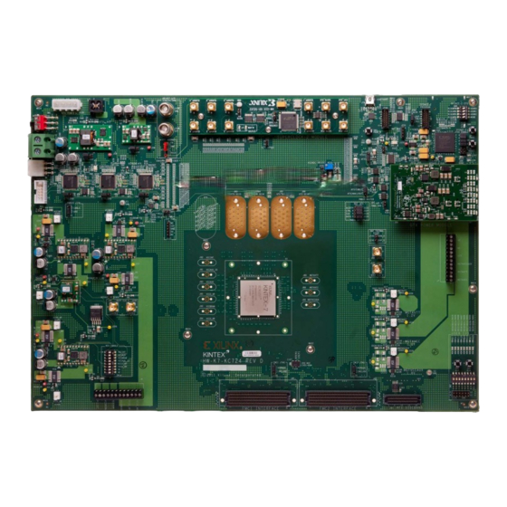
Figure 1-2 is for reference only and might not reflect the current revision of the board. X-Ref Target - Figure 1-2 UG932_c1_02_100312 Figure 1-2: KC724 Board Features. Callouts Listed in Table 1-1 KC724 GTX Transceiver Characterization Board www.xilinx.com Send Feedback UG932 (v2.2) October 10, 2014... - Page 8 User Push Buttons (Active High), page 23 SW4, SW5 J83, J84, J85, J86 GTX transceiver connector pads, page 23 USB-to-UART Bridge, page 28 FMC1 Connector, page 29 FMC2 Connector, page 29 www.xilinx.com KC724 GTX Transceiver Characterization Board Send Feedback UG932 (v2.2) October 10, 2014...
-
Page 9: Power Management
Caution! When powering the board through J2, use only the power supply provided for use with this board (Xilinx part number 3800033). Caution! Do NOT plug a PC ATX power supply 6-pin connector into J2 on the KC724 board. The ATX 6-pin connector has a different pinout than J2. -
Page 10: Onboard Power Regulation
7 Series GTX Power Module MGTAVCC 1.05V at 12.0A max MGTAVTT 1.2V at 8.0A max MGTVCCAUX 1.8V at 2.6A max UG932_c1_03_072712 Figure 1-3: KC724 Board Power Supply Block Diagram www.xilinx.com KC724 GTX Transceiver Characterization Board Send Feedback UG932 (v2.2) October 10, 2014... - Page 11 Fixed LDO regulator, 25 mA VREF_3012 1.25V Notes: 1. The UCD9248PFC (U11) at Address 54 monitors MGTAVCC, MGTAVTT, and MGTVCCAUX rail voltage and current levels through the TI Fusion test application. KC724 GTX Transceiver Characterization Board www.xilinx.com Send Feedback UG932 (v2.2) October 10, 2014...
-
Page 12: Using External Power Sources
J6 (callout 7, Figure 1-2). Caution! The core power terminal block J6 has a maximum load current contact rating of 24A. www.xilinx.com KC724 GTX Transceiver Characterization Board Send Feedback UG932 (v2.2) October 10, 2014... -
Page 13: Disabling Onboard Power
1-2), is provided for use with the TI USB Interface Adapter PMBus pod and associated TI GUI. References More information about the power system components used by the KC724 board are available from the Texas Instruments Digital Power website KC724 GTX Transceiver Characterization Board www.xilinx.com Send Feedback UG932 (v2.2) October 10, 2014... -
Page 14: Series Gtx Transceiver Power Module
7 series GTX modules included with the KC724 board. Table 1-3: 7 Series GTX Transceiver Power Module Power Supply Rail Nominal Voltage Maximum Current Rating Net Name MGTAVCC 1.05V MGTAVTT 1.2V MGTVCCAUX 1.8V 2.6A www.xilinx.com KC724 GTX Transceiver Characterization Board Send Feedback UG932 (v2.2) October 10, 2014... - Page 15 Information about the 7 series GTX power supply modules included with the KC724 kit is available from these vendor websites: • Intersil • Texas Instruments • General Electric KC724 GTX Transceiver Characterization Board www.xilinx.com Send Feedback UG932 (v2.2) October 10, 2014...
-
Page 16: Active Heatsink Power Connector
The fan power connections are detailed in Table 1-4: Table 1-4: Fan Power Connections Fan Wire Header Pin Black J121.1 - GND J121.2 - 12V Blue J121.3 - NC www.xilinx.com KC724 GTX Transceiver Characterization Board Send Feedback UG932 (v2.2) October 10, 2014... -
Page 17: Kintex-7 Fpga
DIP switch (SW8) to select one of eight bitstreams stored on a Secure Digital (SD) memory card (see System ACE SD Configuration Address DIP Switches, page 19). KC724 GTX Transceiver Characterization Board www.xilinx.com Send Feedback UG932 (v2.2) October 10, 2014... -
Page 18: Prog_B Push Button
The DONE LED DS21 (callout 15, Figure 1-2) indicates the state of the DONE pin of the FPGA. When the DONE pin is High, DS21 lights indicating the FPGA is successfully configured. www.xilinx.com KC724 GTX Transceiver Characterization Board Send Feedback UG932 (v2.2) October 10, 2014... -
Page 19: Init Led
Figure 1-11: Configuration Address DIP Switch (SW8) The switch settings for selecting each address are shown in Table 1-5. Table 1-5: SW8 DIP Switch Configuration Configuration Bitstream ADR2 ADR1 ADR0 Address KC724 GTX Transceiver Characterization Board www.xilinx.com Send Feedback UG932 (v2.2) October 10, 2014... -
Page 20: 200 Mhz 2.5V Lvds Oscillator
IOSTANDARD Function Direction Clock recovery Input LVDS_25 CM_LVDS1_P Clock recovery Output Clock recovery Input LVDS_25 CM_LVDS1_N Clock recovery Output Clock recovery Input LVDS_25 CM_LVDS2_P Clock recovery Output www.xilinx.com KC724 GTX Transceiver Characterization Board Send Feedback UG932 (v2.2) October 10, 2014... - Page 21 LVCMOS18 CM_CTRL_20 – Control I/O In/Out LVCMOS18 CM_CTRL_21 – Control I/O In/Out LVCMOS18 CM_CTRL_22 – Control I/O In/Out LVCMOS18 CM_CTRL_23 – CM_RESET Output LVCMOS18 CM_RST RESET_B Input KC724 GTX Transceiver Characterization Board www.xilinx.com Send Feedback UG932 (v2.2) October 10, 2014...
-
Page 22: User Leds (Active High)
User switch Input LVCMOS18 USER_SW4 User switch Input LVCMOS18 USER_SW5 User switch Input LVCMOS18 USER_SW6 User switch Input LVCMOS18 USER_SW7 – User switch Input LVCMOS18 USER_SW8 – www.xilinx.com KC724 GTX Transceiver Characterization Board Send Feedback UG932 (v2.2) October 10, 2014... -
Page 23: User Push Buttons (Active High)
RX-TX lanes. Four lanes are referred to as a Quad. Note: Figure 1-13 is for reference only and might not reflect the current revision of the board. KC724 GTX Transceiver Characterization Board www.xilinx.com Send Feedback UG932 (v2.2) October 10, 2014... - Page 24 Chapter 1: KC724 Board Features and Operation X-Ref Target - Figure 1-13 QUAD_116 QUAD_117 QUAD_115 QUAD_118 UG932_c1_13_062312 Figure 1-13: GTX Quad Locations www.xilinx.com KC724 GTX Transceiver Characterization Board Send Feedback UG932 (v2.2) October 10, 2014...
- Page 25 2,805 115_TX0_N 2,806 115_RX0_P 2,898 115_RX0_N 2,898 115_TX1_P 2,525 115_TX1_N 2,523 115_RX1_P 2,489 115_RX1_N 2,489 115_TX2_P 2,549 115_TX2_N 2,549 115_RX2_P 2,308 115_RX2_N 2,309 115_TX3_P 2,840 115_TX3_N 2,840 KC724 GTX Transceiver Characterization Board www.xilinx.com Send Feedback UG932 (v2.2) October 10, 2014...
- Page 26 2,617 117_TX0_N 2,616 117_RX0_P 2,886 117_RX0_N 2,886 117_TX1_P 2,400 117_TX1_N 2,401 117_RX1_P 2,337 117_RX1_N 2,337 117_TX2_P 2,635 117_TX2_N 2,634 117_RX2_P 2,349 117_RX2_N 2,349 117_TX3_P 2,823 117_TX3_N 2,823 www.xilinx.com KC724 GTX Transceiver Characterization Board Send Feedback UG932 (v2.2) October 10, 2014...
- Page 27 Table 1-13: GTX Transceiver Clock Inputs to the FPGA U1 FPGA Pin Net Name Quad Connector 115_REFCLK0_P 115_REFCLK0_N 115_REFCLK1_P 115_REFCLK1_N 116_REFCLK0_P 116_REFCLK0_N 116_REFCLK1_P 116_REFCLK1_N 117_REFCLK0_P 117_REFCLK0_N 117_REFCLK1_P KC724 GTX Transceiver Characterization Board www.xilinx.com Send Feedback UG932 (v2.2) October 10, 2014...
-
Page 28: Usb-To-Uart Bridge
GROUND Signal ground. The CP2103 supports an I/O voltage range of 1.8V to 3.3V on the KC724 board. Xilinx UART IP is expected to be implemented in the FPGA logic. The FPGA supports the USB-to-UART bridge using four signal pins: •... -
Page 29: Fpga Mezzanine Card Hpc Interface
FMC HPC connectors on the KC724 board tracks the I/O voltage of the FPGA banks that each FMC interface maps to. FMC1 tracks VCCO_HP. FMC2 tracks VCCO_HR. KC724 GTX Transceiver Characterization Board www.xilinx.com Send Feedback UG932 (v2.2) October 10, 2014... - Page 30 FMC1_HA06_P AJ17 FMC1_HA06_N AE16 FMC1_HA07_P AF16 FMC1_HA07_N AJ19 FMC1_HA08_P AK19 FMC1_HA08_N AG19 FMC1_HA09_P AH19 FMC1_HA09_N AJ18 FMC1_HA10_P AK18 FMC1_HA10_N AD19 FMC1_HA11_P AE19 FMC1_HA11_N AD17 FMC1_HA12_P AD16 FMC1_HA12_N www.xilinx.com KC724 GTX Transceiver Characterization Board Send Feedback UG932 (v2.2) October 10, 2014...
- Page 31 AE15 FMC1_HA17_CC_P AE14 FMC1_HA17_CC_N FMC1_HB00_CC_P FMC1_HB00_CC_N FMC1_HB01_P FMC1_HB01_N FMC1_HB02_P FMC1_HB02_N FMC1_HB03_P FMC1_HB03_N FMC1_HB04_P FMC1_HB04_N FMC1_HB05_P FMC1_HB05_N FMC1_HB06_CC_P FMC1_HB06_CC_N FMC1_HB07_P FMC1_HB07_N FMC1_HB08_P FMC1_HB08_N FMC1_HB09_P FMC1_HB09_N FMC1_HB10_P FMC1_HB10_N FMC1_HB11_P KC724 GTX Transceiver Characterization Board www.xilinx.com Send Feedback UG932 (v2.2) October 10, 2014...
- Page 32 FMC1_LA01_CC_P AF11 FMC1_LA01_CC_N AA12 FMC1_LA02_P AB12 FMC1_LA02_N FMC1_LA03_P FMC1_LA03_N FMC1_LA04_P FMC1_LA04_N FMC1_LA05_P FMC1_LA05_N AA11 FMC1_LA06_P AA10 FMC1_LA06_N AA13 FMC1_LA07_P AB13 FMC1_LA07_N AB10 FMC1_LA08_P AC10 FMC1_LA08_N FMC1_LA09_P FMC1_LA09_N www.xilinx.com KC724 GTX Transceiver Characterization Board Send Feedback UG932 (v2.2) October 10, 2014...
- Page 33 AK14 FMC1_LA18_CC_P AK13 FMC1_LA18_CC_N AH14 FMC1_LA19_P AJ14 FMC1_LA19_N AJ13 FMC1_LA20_P AJ12 FMC1_LA20_N AF12 FMC1_LA21_P AG12 FMC1_LA21_N AG13 FMC1_LA22_P AH12 FMC1_LA22_N FMC1_LA23_P FMC1_LA23_N FMC1_LA24_P FMC1_LA24_N FMC1_LA25_P FMC1_LA25_N FMC1_LA26_P KC724 GTX Transceiver Characterization Board www.xilinx.com Send Feedback UG932 (v2.2) October 10, 2014...
- Page 34 U39.10 = U39 pin 10. Table 1-18: VITA 57.1 FMC2 HPC Connections at JA2 U1 FPGA Pin Net Name FMC Pin FMC2_CLK0_M2C_P FMC2_CLK0_M2C_N FMC2_CLK1_M2C_P FMC2_CLK1_M2C_N FMC2_CLK2_BIDIR_P FMC2_CLK2_BIDIR_N FMC2_CLK3_BIDIR_P FMC2_CLK3_BIDIR_N AD23 FMC2_HA00_CC_P www.xilinx.com KC724 GTX Transceiver Characterization Board Send Feedback UG932 (v2.2) October 10, 2014...
- Page 35 FMC2_HA08_P AH24 FMC2_HA08_N AJ24 FMC2_HA09_P AK25 FMC2_HA09_N AE25 FMC2_HA10_P AF25 FMC2_HA10_N AK23 FMC2_HA11_P AK24 FMC2_HA11_N AG25 FMC2_HA12_P AH25 FMC2_HA12_N FMC2_HA13_P FMC2_HA13_N FMC2_HA14_P FMC2_HA14_N FMC2_HA15_P FMC2_HA15_N FMC2_HA16_P FMC2_HA16_N KC724 GTX Transceiver Characterization Board www.xilinx.com Send Feedback UG932 (v2.2) October 10, 2014...
- Page 36 FMC2_HA20_P FMC2_HA20_N FMC2_HA21_P FMC2_HA21_N FMC2_HA22_P FMC2_HA22_N FMC2_HA23_P FMC2_HA23_N FMC2_HB00_CC_P FMC2_HB00_CC_N FMC2_HB01_P FMC2_HB01_N FMC2_HB02_P FMC2_HB02_N FMC2_HB03_P FMC2_HB03_N FMC2_HB04_P FMC2_HB04_N FMC2_HB05_P FMC2_HB05_N FMC2_HB06_CC_P FMC2_HB06_CC_N FMC2_HB07_P FMC2_HB07_N FMC2_HB08_P FMC2_HB08_N FMC2_HB09_P www.xilinx.com KC724 GTX Transceiver Characterization Board Send Feedback UG932 (v2.2) October 10, 2014...
- Page 37 FMC2_HB13_N FMC2_HB14_P FMC2_HB14_N FMC2_HB15_P FMC2_HB15_N FMC2_HB16_P FMC2_HB16_N FMC2_HB17_CC_P FMC2_HB17_CC_N FMC2_HB18_P FMC2_HB18_N FMC2_HB19_P FMC2_HB19_N FMC2_HB20_P FMC2_HB20_N FMC2_HB21_P FMC2_HB21_N U39.11 FMC2_I2C_SCL U39.10 FMC2_I2C_SDA FMC2_LA00_CC_P FMC2_LA00_CC_N FMC2_LA01_CC_P FMC2_LA01_CC_N FMC2_LA02_P FMC2_LA02_N KC724 GTX Transceiver Characterization Board www.xilinx.com Send Feedback UG932 (v2.2) October 10, 2014...
- Page 38 FMC2_LA06_P FMC2_LA06_N FMC2_LA07_P FMC2_LA07_N FMC2_LA08_P FMC2_LA08_N FMC2_LA09_P FMC2_LA09_N FMC2_LA10_P FMC2_LA10_N FMC2_LA11_P FMC2_LA11_N FMC2_LA12_P FMC2_LA12_N FMC2_LA13_P FMC2_LA13_N FMC2_LA14_P FMC2_LA14_N FMC2_LA15_P FMC2_LA15_N FMC2_LA16_P FMC2_LA16_N FMC2_LA17_CC_P FMC2_LA17_CC_N FMC2_LA18_CC_P FMC2_LA18_CC_N FMC2_LA19_P www.xilinx.com KC724 GTX Transceiver Characterization Board Send Feedback UG932 (v2.2) October 10, 2014...
- Page 39 FMC2_LA26_P FMC2_LA26_N FMC2_LA27_P FMC2_LA27_N FMC2_LA28_P FMC2_LA28_N FMC2_LA29_P FMC2_LA29_N FMC2_LA30_P FMC2_LA30_N FMC2_LA31_P FMC2_LA31_N FMC2_LA32_P FMC2_LA32_N FMC2_LA33_P FMC2_LA33_N FMC2_PRSNT_M2C_L FMC1_FMC2_TCK U23.8 U19.2 / U20.1 FMC2_TDI U20.2 / U25.3 FMC2_TDO KC724 GTX Transceiver Characterization Board www.xilinx.com Send Feedback UG932 (v2.2) October 10, 2014...
-
Page 40: Xadc
Jumper pins 2-3 (AGND) on J142: In this configuration, the FPGA's XADC uses an internal reference circuit. Note: A jumper should be installed in one of the two positions during normal operation. www.xilinx.com KC724 GTX Transceiver Characterization Board Send Feedback UG932 (v2.2) October 10, 2014... -
Page 41: I2C Bus Management
MUX as shown in Table 1-20. Table 1-20: I2C Channel Assignments U39 Channel I2C Component SuperClock-2 module 7 series GTX transceiver power supply module FMC1 FMC2 KC724 GTX Transceiver Characterization Board www.xilinx.com Send Feedback UG932 (v2.2) October 10, 2014... - Page 42 Chapter 1: KC724 Board Features and Operation www.xilinx.com KC724 GTX Transceiver Characterization Board Send Feedback UG932 (v2.2) October 10, 2014...
- Page 43 1 through 6 must be set to the ON position as shown in Figure A-1. X-Ref Target - Figure A-1 SW10 Pin 1 VCCINT VCCAUX VCCBRAM VCCAUX_IO VCCO_HP VCCO_HR UG932_aB_01_062812 Figure A-1: Default Switch Settings KC724 GTX Transceiver Characterization Board www.xilinx.com Send Feedback UG932 (v2.2) October 10, 2014...
-
Page 44: Appendix A: Default Jumper And Switch Positions
Appendix A: Default Jumper and Switch Positions www.xilinx.com KC724 GTX Transceiver Characterization Board Send Feedback UG932 (v2.2) October 10, 2014... -
Page 45: Appendix B: Master Constraints File Listing
Appendix B Master Constraints File Listing The KC724 board master Xilinx design constraints file (XDC) template provides for designs targeting the KC724 Kintex-7 FPGA GTX Transceiver Characterization Board. Net names in the constraints listed in this appendix correlate with net names on the KC724 board schematic. - Page 46 PACKAGE_PIN AH10 [get_ports FMC1_LA17_CC_N] set_property IOSTANDARD LVCMOS18 [get_ports FMC1_LA17_CC_N] set_property PACKAGE_PIN AK14 [get_ports FMC1_LA18_CC_P] set_property IOSTANDARD LVCMOS18 [get_ports FMC1_LA18_CC_P] set_property PACKAGE_PIN AK13 [get_ports FMC1_LA18_CC_N] set_property IOSTANDARD LVCMOS18 [get_ports FMC1_LA18_CC_N] www.xilinx.com KC724 GTX Transceiver Characterization Board Send Feedback UG932 (v2.2) October 10, 2014...
- Page 47 IOSTANDARD LVCMOS18 [get_ports FMC1_LA32_P] set_property PACKAGE_PIN AA16 [get_ports FMC1_LA32_N] set_property IOSTANDARD LVCMOS18 [get_ports FMC1_LA32_N] set_property PACKAGE_PIN Y16 [get_ports FMC1_LA33_P] set_property IOSTANDARD LVCMOS18 [get_ports FMC1_LA33_P] set_property PACKAGE_PIN Y15 [get_ports FMC1_LA33_N] KC724 GTX Transceiver Characterization Board www.xilinx.com Send Feedback UG932 (v2.2) October 10, 2014...
- Page 48 IOSTANDARD LVCMOS18 [get_ports FMC1_HA12_N] set_property PACKAGE_PIN Y19 [get_ports FMC1_HA13_P] set_property IOSTANDARD LVCMOS18 [get_ports FMC1_HA13_P] set_property PACKAGE_PIN Y18 [get_ports FMC1_HA13_N] set_property IOSTANDARD LVCMOS18 [get_ports FMC1_HA13_N] set_property PACKAGE_PIN AA18 [get_ports FMC1_HA14_P] www.xilinx.com KC724 GTX Transceiver Characterization Board Send Feedback UG932 (v2.2) October 10, 2014...
- Page 49 IOSTANDARD LVCMOS18 [get_ports FMC1_HB09_P] set_property PACKAGE_PIN AF1 [get_ports FMC1_HB09_N] set_property IOSTANDARD LVCMOS18 [get_ports FMC1_HB09_N] set_property PACKAGE_PIN AG4 [get_ports FMC1_HB10_P] set_property IOSTANDARD LVCMOS18 [get_ports FMC1_HB10_P] set_property PACKAGE_PIN AG3 [get_ports FMC1_HB10_N] KC724 GTX Transceiver Characterization Board www.xilinx.com Send Feedback UG932 (v2.2) October 10, 2014...
- Page 50 PACKAGE_PIN J23 [get_ports FMC2_LA02_P] set_property IOSTANDARD LVCMOS18 [get_ports FMC2_LA02_P] set_property PACKAGE_PIN J24 [get_ports FMC2_LA02_N] set_property IOSTANDARD LVCMOS18 [get_ports FMC2_LA02_N] set_property PACKAGE_PIN L22 [get_ports FMC2_LA03_P] set_property IOSTANDARD LVCMOS18 [get_ports FMC2_LA03_P] www.xilinx.com KC724 GTX Transceiver Characterization Board Send Feedback UG932 (v2.2) October 10, 2014...
- Page 51 IOSTANDARD LVCMOS18 [get_ports FMC2_LA16_N] set_property PACKAGE_PIN U27 [get_ports FMC2_LA17_CC_P] set_property IOSTANDARD LVCMOS18 [get_ports FMC2_LA17_CC_P] set_property PACKAGE_PIN U28 [get_ports FMC2_LA17_CC_N] set_property IOSTANDARD LVCMOS18 [get_ports FMC2_LA17_CC_N] set_property PACKAGE_PIN T25 [get_ports FMC2_LA18_CC_P] KC724 GTX Transceiver Characterization Board www.xilinx.com Send Feedback UG932 (v2.2) October 10, 2014...
- Page 52 PACKAGE_PIN V30 [get_ports FMC2_LA31_N] set_property IOSTANDARD LVCMOS18 [get_ports FMC2_LA31_N] set_property PACKAGE_PIN V25 [get_ports FMC2_LA32_P] set_property IOSTANDARD LVCMOS18 [get_ports FMC2_LA32_P] set_property PACKAGE_PIN W26 [get_ports FMC2_LA32_N] set_property IOSTANDARD LVCMOS18 [get_ports FMC2_LA32_N] www.xilinx.com KC724 GTX Transceiver Characterization Board Send Feedback UG932 (v2.2) October 10, 2014...
- Page 53 PACKAGE_PIN AG25 [get_ports FMC2_HA12_P] set_property IOSTANDARD LVCMOS18 [get_ports FMC2_HA12_P] set_property PACKAGE_PIN AH25 [get_ports FMC2_HA12_N] set_property IOSTANDARD LVCMOS18 [get_ports FMC2_HA12_N] set_property PACKAGE_PIN P24 [get_ports FMC2_HA13_P] set_property IOSTANDARD LVCMOS18 [get_ports FMC2_HA13_P] KC724 GTX Transceiver Characterization Board www.xilinx.com Send Feedback UG932 (v2.2) October 10, 2014...
- Page 54 PACKAGE_PIN K15 [get_ports FMC2_HB02_N] set_property IOSTANDARD LVCMOS18 [get_ports FMC2_HB02_N] set_property PACKAGE_PIN L12 [get_ports FMC2_HB03_P] set_property IOSTANDARD LVCMOS18 [get_ports FMC2_HB03_P] set_property PACKAGE_PIN L13 [get_ports FMC2_HB03_N] set_property IOSTANDARD LVCMOS18 [get_ports FMC2_HB03_N] www.xilinx.com KC724 GTX Transceiver Characterization Board Send Feedback UG932 (v2.2) October 10, 2014...
- Page 55 IOSTANDARD LVCMOS18 [get_ports FMC2_HB17_CC_P] set_property PACKAGE_PIN D13 [get_ports FMC2_HB17_CC_N] set_property IOSTANDARD LVCMOS18 [get_ports FMC2_HB17_CC_N] set_property PACKAGE_PIN C15 [get_ports FMC2_HB18_P] set_property IOSTANDARD LVCMOS18 [get_ports FMC2_HB18_P] set_property PACKAGE_PIN B15 [get_ports FMC2_HB18_N] KC724 GTX Transceiver Characterization Board www.xilinx.com Send Feedback UG932 (v2.2) October 10, 2014...
- Page 56 IOSTANDARD LVCMOS18 [get_ports CM_CTRL_18] set_property PACKAGE_PIN C29 [get_ports CM_CTRL_19] set_property IOSTANDARD LVCMOS18 [get_ports CM_CTRL_19] set_property PACKAGE_PIN A26 [get_ports CM_CTRL_20] set_property IOSTANDARD LVCMOS18 [get_ports CM_CTRL_20] set_property PACKAGE_PIN A25 [get_ports CM_CTRL_21] www.xilinx.com KC724 GTX Transceiver Characterization Board Send Feedback UG932 (v2.2) October 10, 2014...
- Page 57 #SYSTEM CLOCKS set_property PACKAGE_PIN C25 [get_ports LVDS_OSC_P] set_property IOSTANDARD LVDS_25 [get_ports LVDS_OSC_P] set_property PACKAGE_PIN B25 [get_ports LVDS_OSC_N] set_property IOSTANDARD LVDS_25 [get_ports LVDS_OSC_N] #LEDs set_property PACKAGE_PIN A20 [get_ports APP_LED1] KC724 GTX Transceiver Characterization Board www.xilinx.com Send Feedback UG932 (v2.2) October 10, 2014...
- Page 58 IOSTANDARD LVCMOS18 [get_ports SA2_SDHOST_D2] set_property PACKAGE_PIN D19 [get_ports SA2_SDHOST_D3] set_property IOSTANDARD LVCMOS18 [get_ports SA2_SDHOST_D3] set_property PACKAGE_PIN L18 [get_ports SA2_SDHOST_CMD] set_property IOSTANDARD LVCMOS18 [get_ports SA2_SDHOST_CMD] set_property PACKAGE_PIN E19 [get_ports SA2_SDHOST_CLK] www.xilinx.com KC724 GTX Transceiver Characterization Board Send Feedback UG932 (v2.2) October 10, 2014...
- Page 59 PACKAGE_PIN J8 [get_ports 117_REFCLK1_P] set_property PACKAGE_PIN J7 [get_ports 117_REFCLK1_N] set_property PACKAGE_PIN F2 [get_ports 117_TX3_P] set_property PACKAGE_PIN F1 [get_ports 117_TX3_N] set_property PACKAGE_PIN F6 [get_ports 117_RX3_P] set_property PACKAGE_PIN F5 [get_ports 117_RX3_N] KC724 GTX Transceiver Characterization Board www.xilinx.com Send Feedback UG932 (v2.2) October 10, 2014...
- Page 60 PACKAGE_PIN D6 [get_ports 118_RX1_P] set_property PACKAGE_PIN D5 [get_ports 118_RX1_N] set_property PACKAGE_PIN D2 [get_ports 118_TX0_P] set_property PACKAGE_PIN D1 [get_ports 118_TX0_N] set_property PACKAGE_PIN E4 [get_ports 118_RX0_P] set_property PACKAGE_PIN E3 [get_ports 118_RX0_N] www.xilinx.com KC724 GTX Transceiver Characterization Board Send Feedback UG932 (v2.2) October 10, 2014...
-
Page 61: Appendix C: Vita 57.1 Fmc Connector Pinouts
LA33_N HB20_P HB21_N 12P0V DP6_C2M_N HB17_N_CC LA32_N HB20_N 3P3V DP5_C2M_P VIO_B_M2C VADJ VADJ 3P3V DP5_C2M_N VIO_B_M2C VADJ VADJ 3P3V RES0 UG932_ac_01_061812 Figure C-1: FMC HPC Connector Pinout KC724 GTX Transceiver Characterization Board www.xilinx.com Send Feedback UG932 (v2.2) October 10, 2014... - Page 62 Appendix C: VITA 57.1 FMC Connector Pinouts www.xilinx.com KC724 GTX Transceiver Characterization Board Send Feedback UG932 (v2.2) October 10, 2014...
-
Page 63: Appendix D: Additional Resources
The most up to date information related to the KC724 board and its documentation is available on these websites: Kintex-7 FPGA KC724 Characterization Kit Kintex-7 FPGA KC724 Characterization Kit documentation Kintex-7 FPGA KC724 Characterization Kit Answer Record (AR 43390) These documents provide supplemental material useful with this guide: 7 Series FPGAs Overview DS180... - Page 64 Appendix D: Additional Resources These external websites provide supplemental material useful with this guide: Texas Instruments Digital Power www.xilinx.com KC724 GTX Transceiver Characterization Board Send Feedback UG932 (v2.2) October 10, 2014...
-
Page 65: Appendix E: Regulatory And Compliance Information
This product is designed and tested to conform to the European Union directives and standards described in this section. Declaration of Conformity To view the declaration of conformity online, visit: Kintex-7 FPGA KC724 Declaration of Conformity Directives 2006/95/EC, Low Voltage Directive (LVD) 2004/108/EC, Electromagnetic Compatibility (EMC) Directive... -
Page 66: Markings
This product complies with Directive 2002/95/EC on the restriction of hazardous substances (RoHS) in electrical and electronic equipment. This product complies with CE Directives 2006/95/EC, Low Voltage Directive (LVD) and 2004/108/EC, Electromagnetic Compatibility (EMC) Directive. www.xilinx.com KC724 GTX Transceiver Characterization Board Send Feedback UG932 (v2.2) October 10, 2014...