Table of Contents
Advertisement
GE
Intelligent Platforms
Hardware Reference
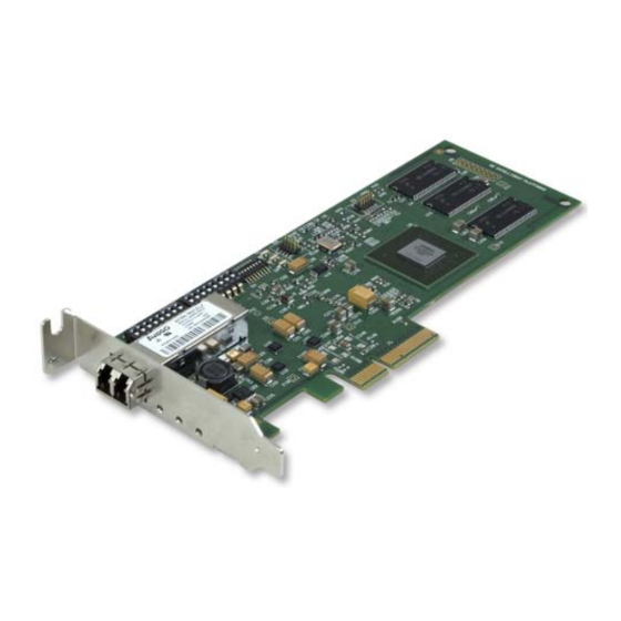
PCIE-5565PIORC*
Ultrahigh Speed Fiber-Optic Reflective Memory
with Interrupts
THE PCIE-5565PIORC IS DESIGNED TO MEET THE EUROPEAN UNION (EU) RESTRICTION OF HAZARD-
OUS SUBSTANCE (ROHS) DIRECTIVE (2002/95/EC) CURRENT REVISIO N.
Publication No: 500-9367875565-000 Rev. A
Advertisement
Table of Contents

Summary of Contents for GE PCIE-5565PIORC*
- Page 1 Intelligent Platforms Hardware Reference PCIE-5565PIORC* Ultrahigh Speed Fiber-Optic Reflective Memory with Interrupts THE PCIE-5565PIORC IS DESIGNED TO MEET THE EUROPEAN UNION (EU) RESTRICTION OF HAZARD- OUS SUBSTANCE (ROHS) DIRECTIVE (2002/95/EC) CURRENT REVISIO N. Publication No: 500-9367875565-000 Rev. A...
- Page 2 Document History 500-9367875565-000 Rev. A September 23, 2011 Hardware Reference Manual Document Number:...
-
Page 3: Table Of Contents
Table of Contents List of Figures ................. 5 List of Tables . - Page 4 3.3.16 Interrupt 4 Sender Data FIFO ............. .59 3.3.17 Interrupt 4 Sender ID FIFO .
-
Page 5: List Of Figures
List of Figures Figure 1 Block Diagram of PCIE-5565PIORC ............. . 9 Figure 2 Typical Reflective Memory Network . -
Page 6: List Of Tables
List of Tables Table 1-1 Example Node ID Switch S2 RFM-5565 ............17 Table 1-2 Switch S1 Configuration RFM-5565 . - Page 7 Table 3-37 Big/Little Endian Descriptor Register ............44 Table 3-38 Interrupt Control and Status Register .
-
Page 8: Overview
Overview The PCIE‐5565PIORC* is a PCI Express (PCIe) member of GE’s family of Reflective Memory real‐time fiber‐optic network products that supports both low profile and standard height PCIe boards. Two or more PCIE‐5565PIORCs, along with other members of this family, can be integrated into a network using standard fiber‐optic cables. Each board in the network is referred to as a “node.” Reflective Memory allows computers, workstations, PLCs and other embedded controllers with different architectures and dissimilar operating systems to share data in real time. The 5565 family of Reflective Memory (referred to as RFM‐5565 in this manual) is fast, flexible and easy to operate. Data is transferred by writing to memory (SDRAM), which appears to reside globally in all boards on the network. Onboard circuitry automatically performs the data transfer to all other nodes with little or no involvement of any host processor. A block diagram of the PCIE‐5565PIORC is shown in Figure 1 on page 9. Features Features include: • High speed, easy to use fiber‐optic network (2.12 Gbaud serially) • x4 lane PCI Express 1 • No host processor involvement in the operation of the network • Selectable Redundant Mode of Operation • Up to 256 nodes • Connectivity with multimode fiber up to 300 m, singlemode fiber up to 10 km • Dynamic packet size, 4 to 64 bytes of data per packet • Fiber network transfer rate 43 MByte/s to 170 MByte/s • 128/256 MBytes SDRAM Reflective Memory with selectable parity • Independent Direct Memory Access (DMA) channel • Four general purpose network interrupts; each with 32 bits of data • Configurable endian conversion for multiple CPU architectures on the same ... -
Page 9: Figure 1 Block Diagram Of Pcie-5565Piorc
PCI Express Compliance The PCIE‐5565PIORC complies with requirements of the PCI Express Specification, Revision 1.1. Vendor and Device Identification The PCI Configuration register reserved for the vendor ID has the value of $114A, which designates GE. The PCI Configuration register reserved for the device ID has the value of $5565, which is GE’s board type. Subsystem Vendor ID and Subsystem ID The PCI Configuration register reserved for the subsystem vendor ID has the value of $1556, which designates PLD Applications. The PCI Configuration register reserved for the subsystem ID has the value of $0080, which is the PLD Applications PCI‐X core identification number. Block Diagram Figure 1 Block Diagram of PCIE-5565PIORC Fiber-Optic Network Optics 2.125 GHz SERDES 16-bit 106.25 MHz FIFO... -
Page 10: Figure 2 Typical Reflective Memory Network
Figure 2 Typical Reflective Memory Network VMIVME-5565 PCI-5565PIORC NODE 0 PCI WorkStation with NODE 1 PCI-5565PIORC VMEbus Chassis with VMIVME-5565 PMC-5565PIORC VMEbus Chassis with NODE 255 PMC-5565PIORC Up to 300m between nodes for multimode Up to 10km between nodes for single mode 10 PCIE-5565PIORC Reflective Memory Board... - Page 11 References PCI Express™ Card Electromechanical Specification Revision 1.1 March 28, 2005 PCI Express Base Specification, Revision 1.1 March 28, 2005 Overview 11...
- Page 12 Organization This manual is composed of the following chapters: Overview provides a general description of the PCIE‐5565PIORC, and General Safety terms and symbols. Chapter 1 Handling and Installation describes unpacking and installation of the hardware. Chapter 2 Theory of Operation describes the product’s features and functionality. Chapter 3 Programming describes PCI Configuration Registers and other registers for programming and installation. Maintenance provides GE’s contact information relative to the care and maintenance of the unit. Compliance provides the applicable information regarding regulatory compliance. 12 PCIE-5565PIORC Reflective Memory Board...
- Page 13 Safety Summary The following general safety precautions must be observed during all phases of the operation, service and repair of this product. Failure to comply with these precautions or with specific warnings elsewhere in this manual violates safety standards of the design, manufacture, and intended use of this product. GE assumes no liability for the customerʹs failure to comply with these requirements. Ground the To minimize shock hazard, the chassis and system cabinet must be connected to System an electrical ground. A three‐conductor AC power cable should be used. The power cable must either be plugged into an approved three‐contact electrical outlet or used with a three‐contact to two‐contact adapter with the grounding wire (green) firmly connected to an electrical ground (safety ground) at the power outlet. Do Not Operate in Do not operate the system in the presence of flammable gases or fumes. Operation an Explosive of any electrical system in such an environment constitutes a definite safety Atmosphere hazard. Keep Away from Operating personnel must not remove product covers. Component replacement Live Circuits and internal adjustments must be made by qualified maintenance personnel. Do not replace components with power cable connected. Under certain conditions, dangerous voltages may exist even with the power cable removed. To avoid injuries, always disconnect power and discharge circuits before touching them. Do Not Service or Do not attempt internal service or adjustment unless another person capable of ...
- Page 14 Warnings, WARNING Cautions WARNING denotes a hazard. It calls attention to a procedure, practice, or and Notes condition, which, if not correctly performed or adhered to, could result in injury or death to personnel. CAUTION CAUTION denotes a hazard. It calls attention to an operating procedure, practice, or condition, which, if not correctly performed or adhered to, could result in damage to or destruction of part or all of the system.
-
Page 15: Handling And Installation
1 • Handling and Installation This chapter describes the installation and configuration of the board. Cable configuration and board layout are illustrated in this chapter. 1.1 Unpacking Procedures Any precautions found in the shipping container should be observed. All items should be carefully unpacked and thoroughly inspected for damage that might have occurred during shipment. The board(s) should be checked for broken components, damaged printed circuit board(s), heat damage and other visible contamination. All claims arising from shipping damage should be filed with the carrier and a complete report sent to GE Technical Support. 1.2 Handling Precaution Some of the components assembled on GE’s products may be sensitive to electrostatic discharge and damage may occur on boards that are subjected to a high‐energy electrostatic field. When the board is placed on a bench for configuring, etc., it is suggested that conductive material should be placed under the board to provide a conductive shunt. Unused boards should be stored in the same protective boxes in which they were shipped. Handling and Installation 15... -
Page 16: Switch S1 And S2 Configuration
1.3 Switch S1 and S2 Configuration Prior to installing the RFM‐5565 in a host system, the desired node ID must be set using switch S2. Each node in the network must have a unique node ID. See Figure 1‐1 on page 18 for the location of switch S2. Switch S2 corresponds to 8 node ID select signal lines. The 8 node ID select lines permit any binary node ID from 0 to $FF (255 decimal). Switch S2 position 1 corresponds to the least significant node ID line and switch S2 position 8 corresponds to the most significant node ID line. Placing switch S2 in the OFF position sets the binary node ID line low (0), while placing switch S2 in the ON position sets the binary node ID line high (1). Table 1‐1 on page 17 provides examples of possible node IDs. 1.3.1 Before Installation Switch S1 and S2 Configuration NOTE ALL nodes on the ring MUST be configured for the SAME transfer mode, either redundant or non- redundant transfer mode. -
Page 17: Table 1-1 Example Node Id Switch S2 Rfm-5565
NOTE S1 position 8 should be set in the ON position only when a flash update of the control logic has failed. After a successful flash update of the control logic, S1 position 8 should be set in the OFF position. -
Page 18: Figure 1-1 S1 And S2 Location Pcie-5565Piorc
Figure 1-1 S1 and S2 Location PCIE-5565PIORC 18 PCIE-5565PIORC Reflective Memory Board... -
Page 19: Physical Installation
1.4 Physical Installation CAUTION Do not install or remove the board while power is applied. Host PCI Express compatible sites vary widely in appearance and board installation procedures. GE recommends examining the host system installation procedures prior to installing this board. The following procedure outlines the installation of the PCIE‐5565PIORC onto a suitable motherboard with an available PCIe connector (x4, x8, or x16). 1. Open the system chassis. Ensure that the node ID has been set prior to instal‐ lation. Also, setup the board for the desired mode of operation. See Section Switch S1 and S2 Configuration on page 16. 2. Install the PCIE‐5565PIORC firmly into the PCIe connector (refer to Figure 1‐ 2 on page 19 for installation of the PCIE‐5565PIORC). Install the screw to secure the PCIE‐5565PIORC to the chassis. 3. Close the system chassis, apply power. Figure 1-2 Installing the PCIE-5565PIORC PCIE-5565PIORC PCIE-5565PIORC Side View Isometric View This PCIE‐5565PIORC comes in two physical form factors: low profile and ... -
Page 20: Front Panel Description
1.5 Front Panel Description The PCIE‐5565PIORC has an optical transceiver and three LEDs located on the front panel illustrated in the figure below. Table 1‐3 on page 21 outlines the front panel’s LEDs. The port labeled “RX” is the receiver and the port labeled “TX” is the transmitter. The PCIE‐5565PIORC uses “LC” type fiber‐optic cables. Figure 1-3 Low Profile and Standard Front Panels of the PCIE-5565PIORC Standard Front Panel Low Profile Front Panel TX TRANSMITTER CONNECTION RX RECEIVER CONNECTION STATUS (RED) SIGNAL DETECT (YELLOW) OWN DATA (GREEN) CAUTION When fiber-optic cables are not connected, the supplied dust caps need to be installed to keep dust and dirt out of the optics. -
Page 21: Led Description
1.5.1 LED Description Table 1-3 LED Descriptions Color Description Status User defined board status indicator. SIG. DET. Yellow Indicates optical network connection. Own Data Green Indicates when own data is received. The status LED’s power up default state is ON. The status LED is a user defined board indicator and can be toggled ON or OFF by writing to Bit 31 of the Control and Status register. The signal detect LED turns ON if the receiver detects light and can be used as a simple method of checking that the optical network is properly connected to the receiver. The Own Data LED is turned ON when the board detects its own data returning over the network. The default setting is OFF. 1.6 Cable Configuration The RFM‐5565 is available with a multimode or singlemode fiber‐optic interface. ... -
Page 22: Figure 1-4 Lc Type Fiber-Optic Cable Connector
Figure 1-4 LC Type Fiber-Optic Cable Connector 0.84 (21.23) (4.5mm) 0.49 (1.25) Dimensions: inches (mm) Figure 1-5 Example: Six Node Ring Connectivity PCIE-5565PIORC Node 1 Node 2 Node 3 Node 4 Node 6 Node 5 22 PCIE-5565PIORC Reflective Memory Board... -
Page 23: Theory Of Operation
2 • Theory of Operation The following sections describe the functionality of the RFM‐5565 Reflective Memory board. A description of the major sub‐circuits and their operation is included. This section will also occasionally mention Control and Status registers related to operations. To see a detailed description of these Control and Status registers please refer to Chapter 3, Programming, on page 29 of this manual. 2.1 Basic Operation Each RFM‐5565 node (any 5565 Reflective Memory board) in the network is interconnected using fiber‐optic cables in a daisy chain loop. The transmitter of the first board must be connected to the receiver of the second board. The transmitter of the second board is connected to the receiver of the third, and so on, until the loop is completed back at the receiver of the first board. Alternatively, any node can be connected to the ring network using one or more ACC‐5595* Reflective Memory Hubs. It is important that the ring network be complete (i.e., every receiver and transmitter must be connected). The RFM‐5565 will not transmit packets if the receiver does not detect a signal or it has lost synchronization (e.g., the cable is damaged). Each node must have a unique node ID, which is set using switch S2 (i.e. no two nodes should have the same node ID). The order of the node IDs is unimportant. A transfer of data over the network is initiated by a write to onboard SDRAM from the host system. The write can be as simple as a PIO target write, or it can be due to a DMA cycle by the resident DMA engine. While the write to the SDRAM is occurring, circuitry on the RFM‐5565 automatically writes the data and other pertinent information into the transmit FIFO. From the transmit FIFO, the transmit circuit retrieves the data and puts it into a variable length packet of 4 to 64 bytes that is transmitted over the fiber‐optic interface to the receiver of the next board. The receiver then checks the packet for errors. When the error free data is received, the receive circuit opens the packet and stores the data in the board’s receive FIFO. From the receive FIFO, another circuit writes the data into the local onboard SDRAM at the same relative location in memory as the originating node. This circuit also simultaneously routes the data into the board’s own transmit FIFO. From there, the process is repeated until the data returns to the receiver of the originating node. At the originating node, the data packet is removed from the network. ... -
Page 24: Rfm-5565 Register Sets
2.3 RFM-5565 Register Sets To go beyond the simple target read and write operation of the board, the user must understand and manipulate bits within three register sets. The three register sets are referred to as: • PCI Configuration Registers • Local Configuration Registers • RFM Control and Status Registers PCI Configuration Registers – This set of registers is predefined by the PCI Local Bus Specification and is standard for all PCI and PCI Express devices. This register set contains the Vendor ID, Device ID, Subsystem Vendor ID and Base Address registers. The PCI Configuration Registers are first initialized and then modified as needed by the PCI bus system BIOS. The register set is rarely altered by the user, but the ability to read these registers, particularly the Base Address Registers, will be necessary to locate the other two sets of registers. Local Configuration Registers – Base Address Register 0 has the starting address for register memory space accesses and Base Address Register 1 has the starting address for register IO space accesses. Some Local Configuration Registers pertinent to the RFM‐5565’s operation include the Interrupt Control and Status Register (INTCSR) and the DMA Control Registers. RFM Control and Status Registers – The RFM Control and Status Registers implement the functions unique to the RFM‐5565 Reflective Memory board. These functions include RFM operation status, detailed control of the RFM sources for the PCI interrupt, and network interrupt access. These registers are accessed at locations offset from the address contained in Base Address Register 2. 2.4 Reflective Memory RAM This board is available with 128 or 256 MByte of onboard Reflective Memory SDRAM. The SDRAM starts at the location specified in Base Address Register 3. Unlike the previous versions of Reflective Memory products, the RFM Control and Status Registers do NOT replace the first $40 locations of RAM. The offset address range is $0 to $7FFFFFF for the 128 MByte and $0 to $FFFFFFF for the 256 MByte option. 24 PCIE-5565PIORC Reflective Memory Board... -
Page 25: Interrupt Circuits
2.5 Interrupt Circuits The RFM‐5565 has a single interrupt output (INTA#). One or more events on the RFM‐5565 board can cause the interrupt. The sources of the interrupt can be individually enabled and monitored through several registers. The interrupt circuitry of the RFM‐5565 is arranged in two tiers. The primary tier of interrupts is enabled and monitored by the Local Configuration Register’s INTCSR at offset $68. The sources for monitoring the primary tier interrupts include: 1. DMA Ch 0 Done 2. Local Interrupt Input (LINTi#) The primary tier interrupt source (1) is used during DMA cycles and must be configured in the DMA registers. The other primary tier interrupt source (2) is the Local Interrupt Input (LINTi#). All secondary tier interrupts are funneled through the LINTi#. Second tier interrupts include several operational status bits, faults, and network interrupts. The second tier interrupts are selected and monitored through the two RFM Control and Status Registers referred to as the Local Interrupt Status Register (LISR) and the Local Interrupt Enable Register (LIER). For a detailed description of these two registers refer to Chapter 3, Programming, on page 29. A block diagram of the main interrupt circuitry is shown in Figure 2‐1 on page 26 . Theory of Operation 25... -
Page 26: Figure 2-1 Interrupt Circuitry Block Diagram
Figure 2-1 Interrupt Circuitry Block Diagram Network Receiver Circuitry RFM Control and Status Registers (per Base Address Register 2) Network Fault/Status Interrupt FIFOs Events Local Interrupt Status Register (LISR) Local Interrupt Enable Register (LIER) (Offset $14) (Offset $10) Second Tier Interrupts LINT# RFM Control and Status Registers (per Base Address Register 0 or 1) -
Page 27: Network Interrupts
2.6 Network Interrupts The RFM‐5565 is capable of passing interrupt packets, as well as data packets, over the network. The network interrupt packets can be directed to a specific node or broadcast globally to all other nodes on the network. Each network interrupt packet contains the sender’s node ID, the destination node ID, the interrupt type and 32 bits of user defined data. The types of network interrupts include four general purpose interrupts and a reset node request interrupt. Node specific interrupts are sent by configuring three RFM Control and Status registers. Each receiving node evaluates the interrupt packets as they pass through. If a general purpose interrupt is directed to that node, then the sender’s node ID is stored in the appropriate Sender ID FIFO (one of four). Each Sender ID FIFO is 127 locations deep. The accompanying data will be stored in a companion 127 locations deep data FIFO. If enabled through the LISR, LIER and INTCSR registers, any of the network interrupts can also generate a host PCI interrupt at each receiving node. The reset node request interrupt is not stored in a FIFO like the four general purpose interrupts. Furthermore, it does not cause an immediate reset of the board. Instead, it sets a bit in the LISR register, which will result in a PCI interrupt if enabled. The actual board reset should be performed by the host system in an orderly fashion. However, the user application could use this network interrupt for any purpose. 2.7 Redundant Transfer Mode of Operation The RFM‐5565 is capable of operating in a redundant transfer mode. The board is configured for redundant mode when switch S1 position 1 is in the ON position. In the redundant transfer mode, each packet transfers twice, regardless of the packet size. The receiving circuitry of each node on the network evaluates each of the redundant transfers. If no errors are detected in the first transfer, it is used to update the onboard memory and the second transfer is discarded. However, if the first transfer contains an error, the second transfer is used to update the onboard memory provided it has no transmission errors. If errors are detected in both transfers, the transfers will not be used and the data is completely removed from the network. Redundant transfer mode reduces the chance that any data is dropped from the network. However, the redundant transfer mode also reduces the network data ... -
Page 28: Rogue Packet Removal Operation
2.8 Rogue Packet Removal Operation A rogue packet is a packet that does not belong to any node on the network. Recalling the basic operation of Reflective Memory, one node originates a packet on the network in response to a memory write from the host. The packet is transferred around the network to all nodes until it returns to the originating node. It is a requirement that the originating node remove the packet from the network. If, however, the packet is erroneously altered as it passes through another node, or if the originating node begins to malfunction, then the originating node may fail to recognize the packet as its own and will not remove it from the network. In this case, the packet will continue to traverse the network as a “rogue packet.” Rogue packets are extremely rare. A rogue packet could be created when turning a node’s power on or off while connected to a 5595 Hub. It could also occur when connecting or disconnecting fiber cables. A rogue packet might be created if any node in the network overflows a network FIFO. Their existence could indicate a malfunctioning board due to true component failure, or due to operation in an overly harsh environment. Normally, the solution is to isolate and replace the malfunctioning board and/or improve the environment. However, some users prefer to tolerate sporadic rogue packets rather than halt the system for maintenance provided the rogue packets are removed from the network. To provide tolerance for rogue packet faults, the RFM‐5565 contains circuitry that allows it to operate as one of two Rogue Masters. A rogue master marks each packet as it passes through from another node. If the same packet returns to the rogue master a second time, the Rogue Master recognizes that it is a rogue packet and removes it from the network (after the rogue packet has affected every node). When a rogue packet is detected, a rogue packet fault flag is set in the LISR. The assertion of the rogue packet fault bit may optionally assert a PCI interrupt to inform the host that the condition exists. Two rogue masters, Rogue Master 0 and Rogue Master 1, are provided to cross check each other. Rogue Master 0 is enabled by placing switch S1 position 5 in the ON position. Rogue Master 1 is enabled by placing switch S1 position 6 in the ON position. Just as two boards in a network should not have the same node ID, two boards in the same network should not be set as the same Rogue Master. Otherwise, one of the two will erroneously remove packets marked by the other. 28 PCIE-5565PIORC Reflective Memory Board... -
Page 29: Programming
3 • Programming Basic target write and read operations of the RFM‐5565 require little or no software. The board powers up in a functional mode. The user will need to access the PCI Configuration registers (Base Address Register 0, 1, 2 and 3) to learn where the system BIOS has located the other register sets and the Reflective Memory. The location of the register sets and the Reflective Memory varies from system to system, and can even vary from slot to slot within a system. For operations beyond the basic setup, such as enabling or disabling interrupts or performing DMA cycles, the user must know the specific bit assignments of the registers within the three register sets. That information is provided in this chapter. The three register sets are: • PCI Configuration Registers • Local Configuration Registers • RFM Control and Status Registers Programming 29... -
Page 30: Pci Configuration Registers
3.1 PCI Configuration Registers The PCI Configuration registers are located in 256 bytes of the PCI Configuration Space, which follows a template defined by the PCI Specification v2.2. The first 64 bytes of the PCI Configuration Space are composed of a fully predefined header. Within that header region, each device implements only the necessary and relevant registers. However, all registers and bit functions within the header region, that are present, must comply with the definitions of the PCI Specification. Beyond the first 64 byte boundary, each device can implement additional device unique registers. Although the PCI Configuration registers are accessible at all times, they are rarely altered by the user. Table 3-1 PCI Configuration Registers Address (Hex) 31..24 23..16 15..8 7..0 Device ID Vendor ID Status Register Command Register Class Code Revision ID BIST Header Type Latency Timer Cache Line Size Base Address Register 0 Base Address Register 1... -
Page 31: Table 3-3 Pci Command Register
Table 3-3 PCI Command Register PCI Command: Offset $04 *Value after Description Read Write PCI Reset I/O Space. Writing a one (1) allows the device to respond to I/O Space accesses. Writing a zero (0) disables the device from responding to I/O Space accesses. -
Page 32: Table 3-4 Pci Status Register
Table 3-4 PCI Status Register PCI Status: Offset $06 Value after Description Read Write PCI Reset Reserved Interrupt Status. Set by the Reflective Memory when the function would normally assert an interrupt pin, regardless of interrupt disable bit state. New Capabilities Functions Support. Hardwired to a one (1). -
Page 33: Table 3-6 Pci Class Code Register
Table 3-6 PCI Class Code Register PCI Class Code: Offset $09 Value after Description Read Write PCI Reset Register Level Programming Interface. None defined. 15:8 Subclass Code 23:16 Base Class Code Base Class Code of $02 equals Network Controller. Subclass Code of $80 equals other network controller. Table 3-7 PCI Cache Line Size Register PCI Cache Line Size: Offset $0C *Value after... -
Page 34: Table 3-10 Pci Built-In Self Test Register
Table 3-10 PCI Built-in Self Test Register PCI Built-in Self Test: Offset $0F Value after Description Read Write PCI Reset BIST Pass/Failed. Writing $0 indicates a device passed its test. Non-$0 values indicate a device failed its test. Device-specific failure codes can be encoded in a non-$0 value. Reserved. -
Page 35: Table 3-12 Pci Base Address Register 1 For Access To Local Configuration Registers
PCI Base Address Register 1 contains the starting address for I/O mapped accesses to Local Configuration Registers. The value in this register is loaded by the system BIOS. Table 3-12 PCI Base Address Register 1 for Access to Local Configuration Registers PCIBAR1: Offset $14 *Value after Description Read Write PCI Reset Memory Space Indicator. A zero (0) indicates the register maps into Memory Space. A one (1) indicates the register maps into I/O Space. (NOTE: Hardcoded to one (1).) Reserved. -
Page 36: Table 3-14 Pci Base Address Register 3 For Access To Reflective Memory
PCI Base Address Register 3 contains the starting address for PIO memory mapped accesses to the Reflective Memory RAM. The value in this register is loaded by the system BIOS. It depends on both the amount of installed SDRAM and the settings of S1 switch positions 3 and 4. The address offset range is: $0 to $01FFFFF for the 2 MByte window setting, $0 to $0FFFFFF for the 16 MByte window setting, $0 to $3FFFFFF for the 64 MByte window setting, $0 to $7FFFFFF for the 128 MByte SDRAM option, and $0 to $FFFFFFF for the 256 MByte option. Table 3-14 PCI Base Address Register 3 for Access to Reflective Memory PCIBAR3: Offset $1C *Value after Description Read Write PCI Reset Memory Space Indicator. Writing zero (0) indicates the register maps into Memory Space. -
Page 37: Table 3-17 Pci Cardbus Cis Pointer Register
Table 3-17 PCI Cardbus CIS Pointer Register PCI Cardbus CIS Pointer: Offset $28 Value after Description Read Write PCI Reset 31:0 Cardbus Information Structure Pointer for PCMCIA. Not Supported. Table 3-18 PCI Subsystem Vendor ID Register PCI Subsystem Vendor ID: Offset $2C *Value after Description Read... -
Page 38: Table 3-22 Pci Interrupt Line
Table 3-22 PCI Interrupt Line PCI Interrupt Line: PCIILR, Offset $3C *Value after Description Read Write PCI Reset Interrupt Line Routing Value. Value indicates which input of the system interrupt controller(s) is connected to each interrupt line of the device. *NOTE: This register will be altered by the system BIOS during the system boot process. -
Page 39: Table 3-26 Power Management Capability Structure
Table 3-26 Power Management Capability Structure Offset 31::24 23::16 15:8 0x078 Capabilities Register (Hardwire to 0x0003) 0x80 Next Cap Ptr 0x01 Capability ID 0x070 Data (hardwired to 0x00) PM Control/Status Bridge Power Management Status and Control Extensions (hardwired to (hardwired to 0x0008) 0xx00) Table 3-27 PCIe Capability Structure Offset... -
Page 40: Table 3-30 Device Control Register Bit Definition
Table 3-29 Device Capabilities Register Bit Definition (Continued) Device Capabilities Register Bit Definition: Offset 0x084 Phantom Functions Not Supported. Hardwired to 00 Supported Max Payload Size Max payload is 256 bytes Supported Table 3-30 Device Control Register Bit Definition Device Control Register Bit Definition: Offset 0x088 Bit(s) Field Description... -
Page 41: Table 3-31 Device Status Register Bit Definition
Table 3-31 Device Status Register Bit Definition Device Status Register Bit Definition: Offset 0x08A Bit(s) Field Description 15:6 Reserved Transactions Pending When set to one, indicates that this function has issued non-posted request packets which have not yet been completed. Aux Power Detected Aux power not required. -
Page 42: Table 3-34 Link Status Register Bit Definition
Table 3-34 Link Status Register Bit Definition Link Status Register Bit Definition: Offset 0x092 Bit(s) Field Description 15:13 Reserved Hardwired to 0x00 Slot Clock 1 = The card uses the reference clock provided on the Configuration connector Link Training 1 = Link Training in process 0 = Link Training done Link Training Error 1 = Link Training Error Occurred... -
Page 43: Local Configuration Registers
3.2 Local Configuration Registers The Local Configuration Registers are memory cycle accessible at the offsets from the value stored in Base Address Register 0. The registers at offsets $00 to $FF are also I/O cycle accessible at the offsets from the value stored in Base Address Register 1. The offsets are specified below. Table 3-35 Local Configuration and DMA Control Registers (Offset from Register Name Writable Base Address) $00-$07 Reserved MARBR (same as $AC) Big/Little Endian Descriptor $10-$67 Reserved INTCSR Reserved PCI H Rev Reserved DMA Channel 0 Mode DMA Channel 0 PCI Address... -
Page 44: Table 3-36 Mode/Dma Arbitration Register
Table 3-36 Mode/DMA Arbitration Register MARBR: BAR0/1 Offset $08 or $AC Value after Description Read Write PCI Reset 23:0 Reserved $040000 Reserved Reserved 31:26 Reserved Table 3-37 Big/Little Endian Descriptor Register BIGEND: BAR0/1 Offset $0C Value after Description Read Write PCI Reset Reserved... -
Page 45: Table 3-38 Interrupt Control And Status Register
Table 3-38 Interrupt Control and Status Register INTCSR: BAR0/1 Offset $68 Value after Description Read Write PCI Reset Reserved PCI Interrupt Enable. Writing a one (1) enables PCI interrupts. 10:9 Reserved Local Interrupt Input Enable. Writing a one (1) enables a local interrupt (i.e., RFM interrupts) to assert a host Interrupt. -
Page 46: Table 3-41 Pci Core/Features Revision Id
Table 3-41 PCI Core/Features Revision ID PCIHREV: BAR0/1 Offset $74 Value after Bits Description Read Write PCI Reset PCI Core/Features Revision ID. This value is read by the Current Rev# RFM-5565 driver to determine the features of this board. Table 3-42 DMA Channel 0 Mode Register DMAMODE0: BAR0/1 Offset $80 Value after Description... -
Page 47: Table 3-45 Dma Channel 0 Transfer Size (Bytes) Register
Table 3-45 DMA Channel 0 Transfer Size (Bytes) Register DMASIZ0: BAR0/1 Offset $8C Value after Description Read Write PCI Reset 22:0 DMA Transfer Size (Bytes). Indicates the number of bytes to transfer during a DMA operation. 31:23 Reserved Table 3-46 DMA Channel 0 Descriptor Pointer Register DMADPR0: BAR0/1 Offset $90 Value after Description... -
Page 48: Table 3-48 Dma Channel 0 Pci Dual Address Cycles Upper Address
Table 3-48 DMA Channel 0 PCI Dual Address Cycles Upper Address DMADAC0: BAR0/1 Offset $B4 Value after Description Read Write PCI Reset 31:0 Upper 32 Bits for 64-bit addressing during DMA Channel 0 Cycles. If set to $0, the DMA performs a 32-bit address DMA Channel 0 access. -
Page 49: Rfm Control And Status Registers
3.3 RFM Control and Status Registers The RFM Control and Status Registers for the RFM‐5565 are memory cycle accessible at the offsets from the value stored in Base Address Register 2. The offsets are specified below. The space reserved for this group of registers is 64 bytes. Table 3-51 Memory Map of the Local Control and Status Registers Offset Mnemonic Description Access Comments Board Revision read only Current board revision/model Board ID Register read only BID is $65 for RFM-5565 $3.2 Board Revision Build read only... -
Page 50: Board Revision Register
3.3.1 Board Revision Register Board Revision (BRV) BAR2 (Offset $0): An 8‐bit register used to represent revisions or model numbers. This register is read‐only. 3.3.2 Board ID Register Board ID (BID) BAR2 (Offset $1): An 8‐bit register which contains an 8‐bit code unique to the RFM‐5565 type boards. The code is $65. This register is read‐only. 3.3.3 Board Revision Build Register Board Revision Build (BRB) BAR2 (Offset $2): A 16‐bit register used to represent the build number for this specific revision. The upper four bits indicate the PCI memory window size corresponding to the FPGA configuration file currently loaded. This register is read‐only. – 1 = 2 MB memory window – 2 = 16 MB memory window – 3 = 64 MB memory window – 4 = 128 MB memory window – 5 = 256 MB memory window 3.3.4 Node ID Register Node ID (NID) BAR2 (Offset $4): An 8‐bit register containing the node ID of the board. This register reflects the setting of the onboard switch S2 and is read‐only. Each board on a network must have a unique node ID. 3.3.5 Local Control and Status Register 1 Local Control and Status Register 1 (LCSR1) BAR2 (Offset $08): A 32‐bit register ... - Page 51 Local Control and Status Register 1 Bit Definitions Bit 31: Status LED – The board contains a user defined RED status LED. Setting this bit low (0) turns OFF the LED. The default state of this bit after reset is high (1) and the LED will be ON. Bit 30: Transmitter Disable – Setting this bit high (1) will manually turn OFF the board’s transmitter. The default state of this bit after reset is low (0) and the transmitter is enabled. When turning the board’s transmitter back ON by setting this bit back to low (0), an unspecified amount of time must be allowed to provide for the turn‐on time of the optics. Bit 29: Dark‐on‐Dark Enable – When this bit is set high (1), the board’s transmitter will be turned OFF if the board’s receiver does not detect a signal or if the receiver detects invalid data patterns. The dark‐on‐dark feature is useful in hub configurations. Bit 28: Loopback Enable – When this bit is set high (1), the fiber optic transmitter and receiver are disabled and the transmit signal is looped back to the receiver circuit internally. This allows basic functional testing with or without an external cable. Bit 27: Local Memory Parity Enable – When this bit is set high (1), parity checking is enabled when reading from the RFM‐5565 SDRAM. Note that parity works only on 32‐bit and 64‐bit accesses. Byte (8‐bit), Word (16‐bit), and 24‐bit memory write accesses are inhibited while parity is enabled. Bit 26: Redundant Mode Enabled – When this bit is set high (1), redundant mode of network transfers has been enabled. This bit is read‐only. Redundant mode is enabled by setting switch S1 position 1 in the ON position. Bit 25: Rogue Master 1 Enabled – When this bit is set high (1), the board is operating as Rogue Master 1. This bit is read‐only. Rogue Master 1 operation is enabled by setting switch S1 position 6 in the ON position. Bit 24: Rogue Master 0 Enabled – When this bit is set high (1), the ...
- Page 52 Window 1 Window 0 PCI PIO Window Size default = installed memory size 64 MByte 16 MByte 2 MByte Bits 21 and 20: Config 1 and Config 0 – These two bits indicate the installed memory size as defined in the following table. The two bits are read‐only. Config 1 Config 0 Memory Size 64 MByte 128 MByte 256 MByte Reserved Bit 18: Delay TX from PCI Write – When this bit is set high (1), the board is operating with reduced PCI write bandwidth. This bit is read‐only. This mode is enabled by setting switch S1 position 2 in the ON position. Data received on the PCI bus ...
- Page 53 Bits 15 through 08: Reserved – These bits are reserved. Bit 07: TX FIFO Empty – A logic high (1) indicates the TX FIFO is currently empty. This bit provides immediate status only (not latched) and is read‐only. Bit 06: TX FIFO Almost Full – A logic high (1) indicates the TX FIFO is currently almost full. This bit provides immediate status only (not latched) and is read‐only. Periodic assertion of this bit is normal. Bit 05: Latched RX FIFO Full – A logic high (1) indicates the RX FIFO has experienced a full condition at least once. This bit is read‐only within this register. To clear this condition write to the corresponding bit within the Local Interrupt Status Register. NOTE The occurrence of the Latched RX FIFO Full signal is a fault condition due to a board malfunction and indicates that the received data may have been lost. Bit 04: ...
-
Page 54: Local Interrupt Control Registers
3.3.6 Local Interrupt Control Registers The RFM‐5565 contains a number of sources for the interrupt. The second tier of interrupts is controlled by two registers called the LISR as shown in Table 3‐53 on page 54 and the LIER shown in Table 3‐54 on page 57. All Local Interrupts are logically “ORed” together into the single interrupt called the LINTi#. The LINTi# line is, in turn, controlled by Bit 11 of the Local Configuration register (INTCSR at offset $68 to Base address 0). The control and status of local interrupts are implemented in the two local registers (LISR and LIER). The bit functions of these two registers mirror each other. Local Interrupt Status Register Local Interrupt Status Register (LISR) BAR2 (Offset $10): This is a 32‐bit register containing a group of interrupt status flags. The LIER contains a corresponding group of enables. Before any local interrupt can cause an interrupt on the LINTi# line, the Status Bit, its Enable and the Global Enable must be asserted. Table 3-53 Local Interrupt Status Register LISR: BAR2 Offset $10 Bit 31 Bit 30 Bit 29 Bit 28 Bit 27 Bit 26 Bit 25 Bit 24... - Page 55 set high (1), the Global Interrupt Enable bit will automatically be cleared as this register (LISR) is being read. This bit is read and write accessible with this register and thus allows a single read‐modify‐write operation to service the local interrupts. Bit 13: Local Memory Parity Error ‐ When this bit is high (1), one or more parity errors have been detected on local memory accesses. This bit is latched. Once set, it must be cleared by writing a zero to this bit location. Note that Bit 27 of the LCSR1 must be set high before parity is active. Also note that parity works only on 32‐bit and 64‐bit accesses. Word (16‐bit) and byte (8‐bit) memory write accesses are inhibited. Bit 12: Memory Write Inhibited ‐ When this bit is high (1), an 8‐bit byte, a 16‐bit word, or a 24‐bit write to local memory was attempted and inhibited while the board was in the parity enabled mode. This bit is latched. Once set, it must be cleared by writing a zero to this bit location. Bit 11: Latched Sync Loss – When this bit is high (1), the receiver circuit has lost synchronization with the incoming signal one or more times. This bit is latched. Once set, it must be cleared by writing a zero to this bit location. The assertion of the Latched Sync Loss usually indicates the receiver link was or is disconnected, either intentionally or unintentionally, and data may have been lost. This event will also occur if the upstream node tied to the receiver is powered off or is disabled. Bit 10: RX FIFO Full – When this bit is high (1), the RX FIFO has been full one or more times. This bit is latched. Once set, it must be cleared by writing a zero to this bit location. This is a fault condition and data may have been lost. NOTE This condition should not occur during normal operation. Bit 10 is for diagnostic purposes only. Bit 09: ...
- Page 56 Bit 07: Pending Net. Int. 4 – When this bit is high (1), one or more type 4 network interrupts have been received. To see the sender data and sender node ID, read the Interrupt Sender Data 4 (ISD4) FIFO at offset $38 and the Interrupt Sender ID (SID4) at offset $3C respectively. Bit 06: Rogue Packet Fault ‐ When this bit is set high (1), the board is operating as either Rogue Master 1 or 0 and has detected and removed a rogue packet. This bit is latched. Once set, it must be cleared by writing a zero (0) to this bit location. Bit 05: TX FIFO Full ‐ When this bit is high (1), the TX FIFO has been full one or more times. This bit is latched. Once set, it must be cleared by writing a zero (0) to this bit location. This is a fault condition and data may have been lost. NOTE This condition should not occur during normal operation. Bit 05 is for diagnostic purposes only. Bit 04: Reserved ‐ This bit is reserved. Bit 03: Reset Node Request – When this bit is high (1), another node on the network has requested that the local PCI bus master reset this board. The RFM‐5565 does not reset itself automatically. Bit 02: Pending Net. Int. 3 – When this bit is high (1), one or more ...
-
Page 57: Network Target Data Register
Local Interrupt Enable Register Local Interrupt Enable Register (LIER) BAR2 (Offset $14): A 32‐bit register containing a group of interrupt enables corresponding to the status bits in LISR. Table 3-54 Local Interrupt Enable Register LIER: BAR2 Offset $14 Bit 31 Bit 30 Bit 29 Bit 28 Bit 27 Bit 26 Bit 25 Bit 24 Reserved Bit 23 Bit 22 Bit 21 Bit 20 Bit 19 Bit 18 Bit 17... -
Page 58: Network Interrupt Command Register
3.3.9 Network Interrupt Command Register Network Interrupt Command (NIC) BAR2 (Offset $1D): An 8‐bit register containing a four‐bit code that defines the type of network interrupt issued. See Table 3‐55 on page 58 for a definition of the possible codes. The NIC is both read and write accessible. Only writing to the NIC register will initiate the network interrupt. The network interrupt is transmitted in order following after all previously written data. Table 3-55 Network Interrupt Command Register NIC: BAR2 Offset $1D NIC[3,2,1,0] Function X000 Reset Node Request (sets LISR Bit 03 only, the user application must perform the actual reset) X001 Network Interrupt 1 (stored in a 127 deep FIFO at the receiving node) X010... -
Page 59: Interrupt 2 Sender Data Fifo
network interrupts are pending, examine bits 07, 02, 01 and 00 in the LISR register. 3.3.12 Interrupt 2 Sender Data FIFO Interrupt 2 Sender Data FIFO (ISD2) BAR2 (Offset $28): A 32‐bit FIFO functioning just like ISD1, except it responds only to type 2 network interrupts. 3.3.13 Interrupt 2 Sender ID FIFO Interrupt 2 Sender ID FIFO (SID2) BAR2 (Offset $2C): An 8‐bit FIFO functioning just like SID1, except it responds only to type 2 network interrupts. 3.3.14 Interrupt 3 Sender Data FIFO Interrupt 3 Sender Data FIFO (ISD3) BAR2 (Offset $30): A 32‐bit FIFO functioning just like ISD1, except it responds only to type 3 network interrupts. 3.3.15 Interrupt 3 Sender ID FIFO Interrupt 3 Sender ID FIFO (SID3) BAR2 (Offset $34): An 8‐bit FIFO functioning just like SID1, except it responds only to type 3 network interrupts. 3.3.16 Interrupt 4 Sender Data FIFO Interrupt 4 Sender Data FIFO (ISD4) BAR2 (Offset $38): A 32‐bit FIFO functioning ... -
Page 60: Figure 3-1 Block Diagram Of The Network Interrupt Reception Circuitry
Figure 3-1 Block Diagram of the Network Interrupt Reception Circuitry Network Transmitter Receiver Network Input Circuitry Circuitry Output Interrupt Detection and Routing Circuitry Network Network Network Network Network Network Network Network Interrupt 1 Interrupt 1 Interrupt 2 Interrupt 2 Interrupt 3 Interrupt 3 Interrupt 4 Interrupt 4... -
Page 61: Example Of A Block Dma Operation For Rfm-5565
3.4 Example of a Block DMA Operation for RFM-5565 1. Base Address Register 0 stores the starting address of the Local Control and Configuration registers, which include the DMA Control registers. The value in this register is PCIBAR0. 2. There are six DMA registers that must be configured to set up the DMA cycle. These DMA registers will remain unchanged after the DMA cycle. DMA channel 0 mode setting: DMAMODE0 at PCIBAR0 + offset $80 Bit 9 set to 0 indicates the use of normal Block DMA (not Scatter/Gather mode). DMA channel 0 PCI starting address: DMAPADR0 at PCIBAR0 + offset $84 Set to the starting address of the PC memory (for either source or destination transfer). DMA channel 0 local starting address: DMALADR0 at PCIBAR0 + offset $88 Set to the starting address of the local (RFM) memory (for either source or destination transfers). NOTE: The first local (RFM) memory location is at $0. DMA channel 0 transfer size: DMASIZ0 at PCIBAR0 + offset $8C Set to the number of bytes to be transferred (maximum $7FFFFF). DMA channel 0 Descriptor Pointer: DMADPR0 at PCIBAR0 + offset $90 Set to $0 for PCI‐to‐Local or set to $8 for Local‐to‐PCI. DMA channel 0 PCI DAC upper address: DMADAC0 at PCIBAR0 + offset $B4 This register is set to $0 when using 32‐bit ... -
Page 62: Example Of A Scatter-Gather Dma Operation For Rfm-5565
3.5 Example of a Scatter-Gather DMA Operation for RFM-5565 Scatter‐Gather DMA transfer is a mode usually used to perform large data transfers separated into multiple smaller pages or blocks. Note that a data page must not cross a 4 GByte address boundary. The DMA descriptor pointer is the address for a chained list of page descriptors. Each page descriptor defines the address and size of a data block plus a pointer to the next descriptor block. The descriptors are automatically fetched when needed and then data is read/written to the corresponding page. The descriptor chain is processed until the data transfer is finished or the end of the descriptor chain is reached, whichever comes first. Page descriptor blocks cannot be mapped in 64‐bit addressing space. The first descriptor must be on a 16‐byte boundary. For best performance, each descriptor block should be aligned on a 16‐byte or 8‐byte boundary. A descriptor chain must be created in PCI 32‐bit memory space before starting a Scatter‐Gather DMA. Each descriptor in the chain has this format: 1st Dword: Lower 32‐bit PCI Address for Data (each page must be aligned on an 8‐byte boundary), 2nd Dword: Upper 32‐bit PCI Address for Data ($0 for 32‐bit addressing), 3rd Dword: Number of bytes to transfer to/from PCI Address (each page size must be a multiple of 8 bytes), 4th Dword: PCI Address of Next Descriptor (write $1 in this field to denote end of chain) Also, keep a total for the size of all data blocks pointed to by the chain. This total length value must be written to the DMA transfer size register. 1. Base Address Register 0 stores the starting address of the Local Control and Configuration registers, which include the DMA Control registers. The value in this register is PCIBAR0. 2. There are six DMA registers that must be configured to set up the DMA cycle. These registers will remain unchanged after the DMA cycle. 62 PCIE-5565PIORC Reflective Memory Board... - Page 63 DMA channel 0 mode setting: DMAMODE0 at PCIBAR0 + offset $80 Bit 9 set to 1 indicates the use of Scatter‐ Gather DMA (not normal Block mode). DMA channel 0 PCI starting address: DMAPADR0 at PCIBAR0 + offset $84 This register is unused during Scatter‐ Gather DMA. DMA channel 0 local starting address: DMALADR0 at PCIBAR0 + offset $88 Set to the starting address of the local (RFM) memory (for either source or destination transfers). NOTE: The first local (RFM) memory location is at $0. DMA channel 0 transfer size: DMASIZ0 at PCIBAR0 + offset $8C Set to the total number of bytes to be transferred in all blocks (maximum $7FFFFF). DMA channel 0 Descriptor Pointer: DMADPR0 at PCIBAR0 + offset $90 Set bits 31:4 to the PCI Address of the first DMA Scatter‐Gather descriptor location. Set bit‐3 to 0 for PCI‐to‐Local or set bit‐3 to 1 for Local‐to‐PCI. DMA channel 0 PCI DAC upper address: DMADAC0 at PCIBAR0 + offset $B4 This register is unused during Scatter‐ Gather DMA. 3. To initiate and monitor the transfer, access DMACSR0 as follows: DMA channel 0 Command/Status register: DMACSR0 at PCIBAR0 + offset $A8. Write $0003 to start the transfer, then poll the same register. When Bit 4 is high (1), the DMA cycle is complete. NOTE Polling read cycles take priority over the DMA cycles. Overly aggressive polling will slow the DMA transfer.
-
Page 64: Example Of A Pci Pio Sliding Window Operation For Rfm-5565
3.6 Example of a PCI PIO Sliding Window Operation for RFM-5565 RFM‐5565 cards are currently available with 128 or 256 MByte of installed memory. Under some circumstances, it is useful to reduce the PCI memory address space window size. For example, a BIOS may have difficulty dividing the address space into enough windows with appropriate granularity for all of the installed devices. In another example, the operating system may not be able to assign resources for all of the drivers loaded. Reducing the PCI window size allows the RFM‐5565 to use a smaller footprint on the PCI bus address space. However, changing the PCI PIO window size does not affect other functions of the card. All of the installed memory on the card can be updated by data packets on the Reflective Memory network. For example, a 256 MByte card will reflect every value written in the 256 MByte Reflective Memory network address space. Also, the RFM‐5565 DMA engine can be used to access every byte of the memory installed on the card. It is also possible to move (remap) the PCI PIO window to access every byte of the memory installed on the card using PIO accesses. Here is a brief description of selecting the PCI memory window size. There are four possible choices: 2 MByte, 16 MByte, 64 MByte or use the default full memory size. Two switches on S1 are used to configure the PCI memory window size. The switch settings should only be changed while the power is off. Use S1 switch positions 3 and 4 to select one of the four window sizes. Bits 20 and 21 of RFM register LCSR1 (PCIBAR2 Offset $08) indicate the full installed memory size. Bit 19 of LCSR1 is connected to S1 switch position 3 and bit 22 of LCSR1 is connected to S1 switch position 4. Both bits 19 and 22 can be read by software (‘1’ when on, ‘0’ when off). The table below lists the number of PCI PIO window selections available with various RFM‐5565 memory options. PCI PIO Number of Number of Number of Switch S1 Switch S1... - Page 65 space. This gives the user application PIO access to the Reflective Memory locations $00000000 up to $001FFFFF. The user application can set the Local Base Address (Remap) register pointing to any valid window in the installed memory. For example, the user application can write $00200000 to the Remap register to access the second 2 MByte PCI PIO window. The register value will be $00200001 since bit‐0 is hardwired to 1. This gives the user application PIO access to the Reflective Memory locations $00200000 up to $003FFFFF. The user application uses the same PCIBAR3 window ranging from $F7600000 up to $F77FFFFF. NOTE After writing a new value to the LAS1BA remap register, the user application should read the LAS1BA remap register before accessing the new window. This ensures the new window mapping has taken effect and subsequent memory accesses will be to the new memory window. In summary, register LAS1RR is the range register corresponding to the size of the ...
-
Page 66: Example Of Network Interrupt Handling
3.7 Example of Network Interrupt Handling The following is an example of the steps necessary to set up the RFM‐5565 to generate a PCI interrupt in response to one of the four basic network interrupts. This example also lists the steps necessary to service that interrupt. When using this example, it is advisable to examine Figure 2‐1 on page 26 and Figure 3‐1 on page 60 to obtain a visual sense of the circuitry involved. 3.7.1 Setup 1. Clear any prior unscheduled interrupts in the SID1 FIFO by writing zero (0) to the SID1 at PCIBAR2 + offset $24. 2. Clear any prior unscheduled interrupts in the SID2 FIFO by writing zero (0) to the SID2 at PCIBAR2 + offset $2C. 3. Clear any prior unscheduled interrupts in the SID3 FIFO by writing zero (0) to the SID3 at PCIBAR2 + offset $34. 4. Clear any prior unscheduled interrupts in the SID4 FIFO by writing zero (0) to the SID4 at PCIBAR2 + offset $3C. 5. Using a read‐modify‐write operation, set Bit 07, Bit 02, Bit 01 and Bit 00 high (1) in the LIER register at PCIBAR2 + offset $14. This allows any one of the four basic network interrupts to assert the onboard signal LINTi#, provided the global enable in the LISR is also high (1). 6. Write the value $4000 to the LISR register at PCIBAR2 + offset $10. The value $4000 sets the Global Interrupt Enable (Bit 14) high (1) and clears any unre‐ lated sources. You may prefer to use a read‐modify‐write operation if other sources in the LISR are to remain unchanged. 7. Using a read‐modify‐write operation, set Bit 8 and Bit 11 high (1) in the INTCSR register at PCIBAR0 + offset $68. Bit 8 is the PCI Interrupt Enable and Bit 11 is the Local Interrupt Input (LINTi#) Enable. 3.7.2 Servicing Network Interrupts Read the INTCSR register at PCIBAR0 + offset $68. Verify that the Local Interrupt ... -
Page 67: Maintenance
Maintenance If a GE product malfunctions, please verify the following: 1. Software version resident on the product 2. System configuration 3. Electrical connections 4. Jumper or configuration options 5. Boards are fully inserted into their proper connector location 6. Connector pins are clean and free from contamination 7. No components or adjacent boards were disturbed when inserting or remov‐ ing the board from the chassis 8. Quality of cables and I/O connections If products must be returned, contact GE for a Return Material Authorization (RMA) Number. This RMA Number must be obtained prior to any return. www.ge-ip.com/rma RMA request forms can be obtained from: GE Technical Support is available at: 1‐800‐433‐2682 in North America, or +1‐780‐401‐7700 for international calls. Requests for Technical Support can be support.huntsville.ip@ge.com sent to: www.ge‐ip.com Or, visit our website: Maintenance Prints User level repairs are not recommended. The drawings and diagrams in this manual are for reference purposes only. Maintenance 67... -
Page 68: Compliance Information
Compliance Information This chapter provides the applicable information regarding regulatory compliance for the PCIE‐5565PIORC. The PCIE‐5565PIORC has met the requirements for compliance to the following standards: GE has evaluated the PCIE‐5565PIORC has met the requirements for compliance to the following standards: • EN55024 • EN55022, Class A • EN60950‐1:2006 International Compliance It has also met the following international levels. European Union • EN 55024:1998/A1:2001/A2:2003 ITE • EN 55022:2006/A1:2007 (Class A) • EN 60950‐1:2006 United States • FCC 47 CFR Part 15 Class A • UL 60950‐1 (2nd Edition) Australia/New Zealand • AS/NZS CISPR 22:2006 Class A ITE • EN55022 :2006/A1:2007 (Class A) Japan • VCCI (April 2005) Class A using: Canada • ... - Page 69 FCC Part 15 This device complies with Part 15 of the FCC Rules. Operation is subject to the following two conditions: (1) this device may not cause harmful interference, and (2) this device must accept any interference received, including interference that may cause undesired operation. FCC Class A NOTE This equipment has been tested and found to comply with the limits for a Class A digital device, pursuant to Part 15 of the FCC Rules. These limits are designed to provide reasonable protection against harmful interference when the equipment is operated in a commercial environment.
- Page 70 © 2011 GE Intelligent Platforms Embedded Systems, Inc. All rights reserved. Information Centers For more information, please visit * indicates a trademark of GE Intelligent Platforms, Inc. and/or its affiliates. All other the GE Intelligent Platforms Embedded Americas: trademarks are the property of their respective...