Sign In
Upload
Manuals
Brands
Xilinx Manuals
Transceiver
Virtex-6 FPGA
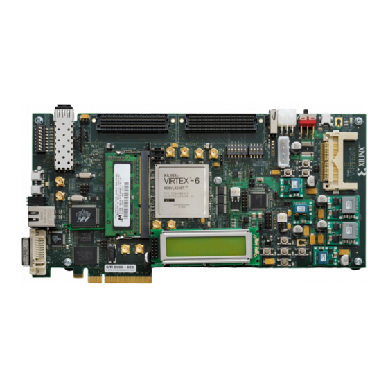
Xilinx Virtex-6 FPGA Development Board Manuals
Manuals and User Guides for Xilinx Virtex-6 FPGA Development Board. We have
10
Xilinx Virtex-6 FPGA Development Board manuals available for free PDF download: Manual, User Manual, Getting Started Manual, Getting Started, Hardware Setup Manual
Xilinx Virtex-6 FPGA User Manual (317 pages)
GTX Transceivers
Brand:
Xilinx
| Category:
Transceiver
| Size: 11.4 MB
Table of Contents
Revision History
3
Table of Contents
9
Preface: about this Guide
17
Guide Contents
17
Additional Documentation
17
Additional Resources
18
Additional References
18
Chapter 1: Transceiver and Tool Overview
19
Overview
19
Port and Attribute Summary
23
Virtex-6 FPGA GTX Transceiver Wizard
36
Simulation
37
Functional Description
37
Ports and Attributes
38
Sim_Gtxreset_Speedup
39
Sim_Receiver_Detect_Pass
40
Sim_Rxrefclk_Source
40
Sim_Txrefclk_Source
40
Sim_Version
41
Sim_Tx_Elec_Idle_Level
41
Implementation
41
Functional Description
41
FF484 Package Placement Diagrams
42
FF784 Package Placement Diagrams
44
FF1156 Package Placement Diagrams
47
FF1759 Package Placement Diagrams
52
FF1154 Package Placement Diagrams
61
FF1155 Package Placement Diagrams
73
FF1923 Package Placement Diagrams
79
FF1924 Package Placement Diagrams
89
Chapter 2: Shared Transceiver Features
101
Reference Clock Input Structure
101
Functional Description
101
Ports and Attributes
101
Use Modes: Reference Clock Termination
102
Reference Clock Selection
102
Functional Description
102
Ports and Attributes
106
Single External Reference Clock Use Model
108
Multiple External Reference Clocks Use Model
110
Pll
113
Functional Description
113
Ports and Attributes
115
PLL Settings for Common Protocols
117
Power down
120
Functional Description
120
Ports and Attributes
120
Generic Power-Down Capabilities
121
PLL Power down
122
TX and RX Power down
122
Power-Down Requirements for TX and RX Buffer Bypass
122
Power-Down Features for PCI Express Operation
123
Loopback
123
Functional Description
123
Ports and Attributes
124
Acjtag
125
Functional Description
125
Dynamic Reconfiguration Port
125
Ports and Attributes
126
Chapter 3 : Transmitter
127
TX Overview
127
FPGA TX Interface
128
Functional Description
128
Interface Width Configuration
128
TXUSRCLK and TXUSRCLK2 Generation
129
Ports and Attributes
130
Using TXOUTCLK to Drive the GTX TX
131
TXOUTCLK Driving a GTX TX in 2-Byte Mode (Single Lane)
131
TXOUTCLK Driving a GTX TX in 4-Byte Mode (Single Lane)
132
TXOUTCLK Driving a GTX TX in 1-Byte Mode (Single Lane)
133
TXOUTCLK Driving more than One GTX TX in 2-Byte Mode (Multiple Lanes)
133
TXOUTCLK Driving more than One GTX TX in 4-Byte Mode (Multiple Lanes)
134
TXOUTCLK Driving more than One GTX TX in 1-Byte Mode (Multiple Lanes)
135
TX Initialization
136
Functional Description
136
Ports and Attributes
138
GTX TX Reset in Response to Completion of Configuration
139
GTX TX Reset in Response to GTXTXRESET Pulse
139
GTX TX Component-Level Resets
140
After Power-Up and Configuration
142
After Turning on a Reference Clock to the TX PLL
142
After Changing the Reference Clock to the TX PLL
142
After Assertion/Deassertion of TXPOWERDOWN
142
TX Rate Change with the TX Buffer Enabled
142
TX Rate Change with the TX Buffer Bypassed
142
TX Parallel Clock Source Reset
142
TX 8B/10B Encoder
143
Functional Description
143
8B/10B Bit and Byte Ordering
143
K Characters
144
Running Disparity
144
Ports and Attributes
144
Enabling and Disabling 8B/10B Encoding
146
TX Gearbox
146
Functional Description
146
Ports and Attributes
146
Enabling the TX Gearbox
147
TX Gearbox Bit and Byte Ordering
147
TX Gearbox Operating Modes
148
External Sequence Counter Operating Mode
149
Internal Sequence Counter Operating Mode
151
TX Buffer
153
Functional Description
153
Ports and Attributes
154
Using the TX Buffer
154
Using the TX Buffer for Oversampling Mode
154
TX Buffer Bypass
155
Functional Description
155
Ports and Attributes
155
Using the TX Phase-Alignment Circuit to Bypass the Buffer
158
TX Phase Alignment after Rate Change Use Mode
159
Using the TX Phase Alignment Circuit to Minimize TX Lane-To-Lane Skew
160
Transmit Fabric Clocking Use Model for TX Buffer Bypass
161
TX Pattern Generator
162
Functional Description
162
Ports and Attributes
164
Use Models
164
TX Oversampling
166
Functional Description
166
Ports and Attributes
166
TX Polarity Control
166
Using TX Polarity Control
166
TX Fabric Clock Output Control
167
Functional Description
167
Serial Clock Divider
168
Parallel Clock Divider and Selector
168
Ports and Attributes
169
PCI Express Clocking Use Mode
170
Rate Change Use Mode for PCI Express 2.0 Operation
171
TX Configurable Driver
172
Functional Description
172
Ports and Attributes
173
Use Modes - TX Driver
178
General
178
Pcie Mode
178
Customizable User Presets
178
Use Mode - Resistor Calibration
178
TX Receiver Detect Support for PCI Express Designs
179
Functional Description
179
Ports and Attributes
179
TX Out-Of-Band Signaling
180
Functional Description
180
Ports and Attributes
181
Chapter 4: Receiver
183
RX Overview
183
RX Analog Front End
184
Functional Description
184
Ports and Attributes
185
Use Modes - RX Termination
186
Use Mode - Resistor Calibration
191
RX Out-Of-Band Signaling
192
Functional Description
192
Ports and Attributes
192
RX Equalizer
194
Functional Description
194
Ports and Attributes
197
Use Mode - Continuous Time RX Linear Equalizer Only
199
Use Mode - Fixed Tap Mode
199
Use Mode - Auto-To-Fix
203
Use Mode - Auto
203
Rx Cdr
204
Functional Description
204
Ports and Attributes
205
RX Fabric Clock Output Control
207
Functional Description
207
Serial Clock Divider
208
Parallel Clock Divider and Selector
208
Ports and Attributes
209
RX Margin Analysis
210
Functional Description
210
Horizontal Eye Margin Scan
210
Eye Outline Scan Mode
212
Ports and Attributes
212
RX Polarity Control
213
Functional Description
213
Ports and Attributes
213
Using RX Polarity Control
213
RX Oversampling
214
Feature Description
214
Ports and Attributes
215
RX Pattern Checker
215
Functional Description
215
Ports and Attributes
216
Use Models
216
RX Byte and Word Alignment
217
Functional Description
217
Enabling Comma Alignment
218
Configuring Comma Patterns
218
Activating Comma Alignment
219
Alignment Status Signals
219
Alignment Boundaries
220
Manual Alignment
220
Ports and Attributes
222
RX Loss-Of-Sync State Machine
226
Functional Description
226
Ports and Attributes
227
RX 8B/10B Decoder
228
Functional Description
228
8B/10B Decoder Bit and Byte Order
228
RX Running Disparity
229
Ports and Attributes
230
RX Buffer Bypass
231
Functional Description
231
Ports and Attributes
232
Using the RX Phase Alignment Circuit to Bypass the Buffer
235
RX Elastic Buffer
238
Functional Description
238
Ports and Attributes
239
Rx_Buffer_Use
239
Boolean Use or Bypass the RX Elastic Buffer
239
TRUE: Use the RX Elastic Buffer (Normal Mode)
239
FALSE: Permanently Bypass the RX Elastic Buffer (Advanced Feature)
239
Using the RX Elastic Buffer for Channel Bonding or Clock Correction
240
RX Clock Correction
240
Functional Description
240
Ports and Attributes
241
Using RX Clock Correction
245
Enabling Clock Correction
245
Setting RX Elastic Buffer Limits
245
Setting Clock Correction Sequences
245
Clock Correction Options
246
Monitoring Clock Correction
246
RX Channel Bonding
247
Functional Description
247
Ports and Attributes
247
Using RX Channel Bonding
250
Enabling Channel Bonding
250
Channel Bonding Mode
250
Connecting Channel Bonding Ports
251
Setting Channel Bonding Sequences
254
Setting the Maximum Skew
254
Precedence between Channel Bonding and Clock Correction
255
RX Gearbox
256
Functional Description
256
Ports and Attributes
256
Enabling the RX Gearbox
257
RX Gearbox Operating Modes
257
RX Gearbox Block Synchronization
258
RX Initialization
261
Functional Description
261
Ports and Attributes
261
GTX RX Reset in Response to Completion of Configuration
263
GTX RX Reset in Response to GTXRXRESET Pulse
263
Link Idle Reset Support
264
GTX RX Component-Level Resets
264
After Power-Up and Configuration
266
After Turning on a Reference Clock to RX PLL
266
After Changing the Reference Clock to RX PLL
267
After Assertion/Deassertion of RXPOWERDOWN
267
RX Rate Change with RX Elastic Buffer Enabled
267
RX Rate Change with RX Elastic Buffer Bypassed
267
RX Parallel Clock Source Reset
267
After Remote Power-Up
267
Electrical Idle Reset
267
After Connecting RXN/RXP
268
After an RX Elastic Buffer Error
268
Before Channel Bonding
268
After Changing Channel Bonding Mode on the Fly
268
After a PRBS Error
268
After an Oversampler Error
268
After Comma Realignment
269
FPGA RX Interface
269
Functional Description
269
Interface Width Configuration
269
RXUSRCLK and RXUSRCLK2 Generation
270
Ports and Attributes
271
Rx_Data_Width
271
Chapter 5: Board Design Guidelines
273
Overview
273
Pin Description and Design Guidelines
273
GTX Transceiver Pin Descriptions
273
Termination Resistor Calibration Circuit
274
Managing Unused GTX Transceivers
276
Analog Power Supply Pins
276
Unused Quad Column
277
Partially Unused Quad Column
278
Partially Used Quad
279
Quad Usage Priority
279
Reference Clock
280
Overview
280
Reference Clock Checklist
282
Reference Clock Interface
282
Lvds
282
Lvpecl
282
AC Coupled Reference Clock
283
Unused Reference Clocks
283
Reference Clock Power
283
Reference Clock Toggling
283
Power Supply and Filtering
283
Overview
283
Power Supply Regulators
284
Linear Vs. Switching Regulators
284
Linear Regulator
284
Switching Regulator
285
Power Supply Distribution Network
286
Staged Decoupling
286
Power Supply Decoupling Capacitors
286
Printed Circuit Board Design
286
Board Stackup
287
GTX Transceiver Power Connections
288
Signal BGA Breakout
289
Crosstalk
291
Hot Swapping Devices
291
Selectio Usage Guidelines
291
Appendix A: 8B/10B Valid Characters
294
Appendix A: 8B/10B Valid Characters
296
Appendix A: 8B/10B Valid Characters
298
Appendix A: 8B/10B Valid Characters
300
Appendix A: 8B/10B Valid Characters
302
Appendix B: DRP Address Map of the GTX Transceiver
303
Rx_Dlyalign_Ctrinc
314
Rx_Dlyalign_Lpfinc
314
Rx_Dlyalign_Ovrdsetting
314
Appendix C: Low Latency Design
315
GTX TX Latency
316
GTX RX Latency
317
Advertisement
Xilinx Virtex-6 FPGA Manual (381 pages)
Brand:
Xilinx
| Category:
Motherboard
| Size: 7.26 MB
Table of Contents
Section 1
217
Table of Contents
217
I3 I2 I1 I0
219
Inputs I3
219
Vhdlinstantiationtemplate
220
Designentrymethod
220
Instantiation Inference
220
Library UNISIM; Use Unisim.vcomponents.all
220
I0(I0), // LUT Input
221
I1 => I1, -- LUT Input I2 => I2, -- LUT Input I3 => I3
221
I3 => I3 -- LUT Input
221
Virtex-6 Libraries Guide for HDL Designs
221
Section 2
224
Init[14] Init
226
Init[15] Init
226
Outputs OLO
226
Design Entry Method
227
Instantiation Yes
227
Inference Recommended
227
CORE Generator™ and Wizards no
227
Macro Support no
227
Available Attributes
227
Attribute Data Type Values Default Description
227
INIT Hexadecimal any 32-Bit Value All Zeros Specifies the Logic Value for the Look-Up
227
VHDL Instantiation Template
227
Unless They Already Exist, Copy the Following Two Statements and Paste Them before the Entity Declaration
227
I0(I0), // LUT Input
231
I1(I1), // LUT Input
231
I2(I2), // LUT Input
231
I3(I3), // LUT Input
231
I4(I4) // LUT Input
231
Available Attributes
235
For more Information
235
See the Virtex-6 FPGA User Documentation (User Guides and Data Sheets)
235
Virtex-6 Libraries Guide for HDL Designs
235
I0(I0), // LUT Input
235
I1(I1), // LUT Input
235
I2(I2), // LUT Input
235
I3(I3), // LUT Input
235
I4(I4), // LUT Input
235
Xilinx HDL Libraries Guide, Version
235
O(O), // LUT General Output
235
Verilog Instantiation Template
239
Library UNISIM; Use Unisim.vcomponents.all
374
Xilinx Virtex-6 FPGA User Manual (148 pages)
GTH Transceivers
Brand:
Xilinx
| Category:
Transceiver
| Size: 4.24 MB
Table of Contents
Revision History
3
Table of Contents
5
Guide Contents
9
Additional Documentation
9
Additional Resources
10
Chapter 1: Transceiver and Tool Overview
11
Overview
11
Port and Attribute Summary
14
Virtex-6 FPGA GTH Transceiver Wizard
30
Simulation
31
Functional Description
31
Ports and Attributes
31
Implementation
31
FF1155 Package Diagrams
33
FF1923 and FF1924 Package Diagrams
36
Chapter 2: Shared Transceiver Features
43
Reference Clock Input Structure
43
Functional Description
43
Ports and Attributes
44
Using the Reference Clock
44
Reference Clock Distribution and Selection
45
Functional Description
45
Ports and Attributes
45
Clocking from an External Source
46
Clocking from a Neighboring GTH Quad
46
Pll
48
Functional Description
48
Ports and Attributes
52
PLL Settings for the Common Protocol
55
Reset and Initialization
55
Functional Description
55
Ports and Attributes
56
GTH Quad Initialization in Response to Completion of Configuration
60
GTH Quad Reset in Response to GTHRESET
62
Resetting the Transmit Datapath
65
Resetting the Receive Datapath
65
Power down
66
Functional Description
66
Ports and Attributes
66
Using Power down
67
Loopback
67
Functional Description
67
Far-End Loopback
67
Near-End PCS Loopback
68
Near-End PMA Loopback
68
Ports and Attributes
69
Dynamic Reconfiguration Port
70
Functional Description
70
Ports and Attributes
70
Using the DRP Interface
70
Management Interface
71
Functional Description
71
Ports and Attributes
71
Using the Management Interface
72
Chapter 3 : Transmitter
75
FPGA TX Interface
75
Functional Description
75
Ports and Attributes
78
Transmit Clocking
81
Configuring the Transmitter for Multi-Lane Applications
82
TX 8B/10B Block
82
Functional Description
82
Ports and Attributes
82
Enabling 8B/10B Mode
85
TX 64B/66B Block
86
Functional Description
86
Ports and Attributes
86
Enabling 64B/66B Mode
89
TX Raw Mode
89
Functional Description
89
Ports and Attributes
89
Enabling Raw Mode
92
TX Pattern Generator
93
Functional Description
93
Ports and Attributes
93
TX Polarity Control
96
Functional Description
96
Ports and Attributes
96
Using TX Polarity Control
96
TX Configurable Driver
97
Functional Description
97
Ports and Attributes
98
Setting the TX Driver
100
Amplitude (Swing)
100
Post-Cursor Emphasis
100
Pre-Cursor Emphasis
101
Chapter 4: Receiver
104
RX Analog Front End
104
Ports and Attributes
105
Interfacing to the RX AFE
105
RX Equalization
105
Functional Description
105
Ports and Attributes
106
Setting the RX Equalization
108
Agc
108
Dfe
108
Ctle
109
Rx Cdr
109
Functional Description
109
Ports and Attributes
110
RX Polarity Control
111
Functional Description
111
Ports and Attributes
111
Using RX Polarity Control
111
RX Pattern Checker
112
Functional Description
112
Ports and Attributes
113
Using RX Pattern Checker
116
RX Raw Mode
117
Functional Description
117
Ports and Attributes
117
Enabling Raw Mode
121
Using the Barrel Shifter
121
RX 64B/66B Block
122
Functional Description
122
Ports and Attributes
122
Enabling 64B/66B Mode
126
RX 8B/10B Block
126
Functional Description
126
Ports and Attributes
126
Enabling 8B/10B Mode
130
Using Comma Alignment
130
FPGA RX Interface
130
Functional Description
130
Ports and Attributes
132
Receive Clocking
136
Configuring the Receiver for Multi-Lane Applications
137
Chapter 5: Board Design Guidelines
139
Overview
139
Pin Description and Design Guidelines
139
GTH Quad Pin Descriptions
139
Termination Resistor Calibration Circuit
141
Reference Clock
141
Overview
141
GTH Transceiver Reference Clock Checklist
142
Reference Clock Interface
143
Lvpecl
143
AC Coupled Reference Clock
143
Unused Reference Clocks
144
Reference Clock Power
144
Crosstalk
146
Advertisement
Xilinx Virtex-6 FPGA User Manual (92 pages)
Brand:
Xilinx
| Category:
Motherboard
| Size: 3.01 MB
Table of Contents
Revision History
2
Table of Contents
3
Preface: about this Guide
5
Guide Contents
5
Additional Documentation
5
Additional Support Resources
6
Chapter 1: ML605 Evaluation Board
7
Overview
7
Additional Information
7
Features
8
Block Diagram
10
Related Xilinx Documents
10
Detailed Description
11
1 Virtex-6 XC6VLX240T-1FFG1156 FPGA
13
Configuration
13
I/O Voltage Rails
14
2 MB DDR3 Memory SODIMM
15
3 Mb Platform Flash XL
20
4 MB Linear BPI Flash
20
ML605 Flash Boot Options
21
5 System ACE CF and Compactflash Connector
24
6 Usb Jtag
26
7 Clock Generation
27
Oscillator (Differential)
27
Oscillator Socket (Single-Ended, 2.5V)
27
SMA Connectors (Differential)
29
8 Multi-Gigabit Transceivers (GTX Mgts)
31
9 PCI Express Endpoint Connectivity
32
10 SFP Module Connector
35
100 /1000 Tri-Speed Ethernet PHY
36
SGMII GTX Transceiver Clock Generation
37
12 USB-To-UART Bridge
39
13 USB Controller
40
506 DVI Codec
41
15 IIC Bus
42
Kb NV Memory
44
16 Status Leds
45
Ethernet PHY Status Leds
46
FPGA INIT and DONE Leds
47
17 User I/O
47
User Leds
48
User Pushbutton Switches
49
User DIP Switch
50
User SMA GPIO
51
LCD Display (16 Character X 2 Lines)
52
18 Switches
53
Power On/Off Slide Switch SW2
53
FPGA_PROG_B Pushbutton SW4 (Active-Low)
54
SYSACE_RESET_B Pushbutton SW3 (Active-Low)
54
System ACE CF Compactflash Image Select DIP Switch S1
55
Mode, Osc Enable, Boot EEPROM Select, and Addr Select DIP Switch S2
56
19 VITA 57.1 FMC HPC Connector
57
20 VITA 57.1 FMC LPC Connector
63
21 Power Management
65
AC Adapter and Input Power Jack/Switch
65
Onboard Power Regulation
66
22 System Monitor
68
Configuration Options
73
Connector Pinout
77
Xilinx Virtex-6 FPGA User Manual (62 pages)
System Monitor
Brand:
Xilinx
| Category:
Monitor
| Size: 3.1 MB
Table of Contents
Revision History
2
Table of Contents
3
Preface: about this Guide
5
Additional Documentation
5
Additional Support Resources
6
System Monitor Primitive
8
System Monitor Ports
8
User Attributes
10
Pre-Configuration Operation
10
Analog-To-Digital Converter
11
Temperature Sensor
12
Power Supply Sensor
14
Register File Interface
14
Status Registers
15
Flag Register
17
Control Registers
17
Configuration Registers (40H to 42H)
17
Test Registers (43H to 47H)
20
Channel Sequencer Registers (48H to 4Fh)
21
Alarm Registers (50H to 57H)
21
DRP JTAG Interface
21
System Monitor DRP JTAG Write Operation
21
System Monitor JTAG DRP Read Operation
22
JTAG DRP Commands
23
DRP Arbitration
24
Jtagbusy
24
Jtagmodified
24
Jtaglocked
24
System Monitor Control Logic
25
Channel Sequencer
25
ADC Channel Selection (48H and 49H)
26
ADC Channel Averaging (4Ah and 4Bh)
27
ADC Channel Analog-Input Mode (4Ch and 4Dh)
29
ADC Channel Acquisition Time (4Eh and 4Fh)
29
Maximum and Minimum Status Registers
29
Automatic Alarms
29
Supply Sensor Alarms
30
Thermal Management
30
Thermal Diode (DXP and DXN)
31
System Monitor Calibration
31
Calibration Coefficients
32
Calibration Example
32
System Monitor Timing
33
Continuous Sampling
34
Acquisition Phase
34
Conversion Phase
35
Event-Driven Sampling
36
Analog Inputs
39
Auxiliary Analog Inputs
40
Adjusting the Acquisition Time
41
Analog Input Description
41
Unipolar Input Signals
42
Bipolar Input Signals
43
Application Guidelines
45
Reference Inputs (VREFP and VREFN)
45
Analog Power Supply and Ground (AVDD and AVSS)
45
External Analog Inputs
47
Anti-Alias Filters
47
PC Board Design Guidelines
47
Example Instantiation of SYSMON
49
Sysmon I/O
50
SYSMON Attributes
51
Simulation of the SYSMON Design
57
EDK Support for System Monitor
59
Chipscope Pro Tool and System Monitor
60
Xilinx Virtex-6 FPGA Getting Started Manual (77 pages)
Connectivity Kit
Brand:
Xilinx
| Category:
Cables and connectors
| Size: 14.11 MB
Table of Contents
Revision History
2
Table of Contents
5
Preface: about this Guide
7
Additional Resources
7
Additional Support
7
Virtex-6 FPGA Connectivity Kit
9
Introduction
9
Connectivity Kit Contents
9
What Is Inside the Box
9
What Is Available Online
10
Getting Started with the Connectivity Targeted Reference Design Demo
10
Board and Connectivity Targeted Reference Design Features
10
Hardware Demonstration Setup Instructions
12
Install Windows Driver
15
Install Linux Driver
27
Evaluating the Virtex-6 FPGA Connectivity TRD
33
Installation and Licensing of ISE Design Suite
36
Downloading and Installing Tool Licenses
36
Modifying the Virtex-6 FPGA Targeted Reference Design
42
Hardware Modifications
42
Test Setup
44
Software Modifications
45
Windows Driver
45
Linux Driver
56
Next Steps
57
Connectivity TRD Modules
57
PCI Express
58
Packet DMA
59
Multiport Virtual FIFO and Memory Controller Block
60
Xaui
61
Software Device Driver and Software Application/Gui Files and Scripts
62
Simulating the Connectivity TRD
63
Reusing the DMA IP from Northwest Logic
63
Modifications to the Connectivity TRD
63
Getting Started with the Virtex-6 FPGA IBERT Reference Design
64
IBERT Hardware Demonstration Setup Instructions
64
Reference Design Files
75
Installation Is Complete
75
Warranty
76
Xilinx Virtex-6 FPGA Getting Started (72 pages)
Evaluation Kit
Brand:
Xilinx
| Category:
Motherboard
| Size: 9.45 MB
Table of Contents
Table of Contents
3
Preface: about this Guide
5
Additional Documentation
5
Additional Support Resources
6
Introduction
7
ML605 Evaluation Kit Contents
7
Key Features
8
Virtex-6 FPGA
8
Configuration
8
Communication and Networking
8
Memory
8
Clocking
8
Input/Output and Expansion Ports
9
Power
9
Getting Started with the Flash Demonstration
9
Board Features
10
Connecting the Cables and Power
11
Setting the System Properties
12
Configuring the FPGA
15
Running the bist Application
17
Getting Started with PCI Express PIO Demonstration
28
System Requirements, Installation, and Setup
29
Running the PCI Express PIO Demonstration
31
Configuration Registers Test
32
Base Address Register (BAR) Test
38
Getting Started with the Base Reference Design
43
Setting up the Hardware for the Base Reference Design
44
Installing Base Reference Design Application GUI
44
Running the Base Reference Design
55
Installing the ISE Software
61
Redeeming the Software and IP License
62
Now What
67
Getting Additional Help and Support
68
Support
68
Warranty
69
Appendix A: References
71
Xilinx Virtex-6 FPGA Getting Started (36 pages)
Brand:
Xilinx
| Category:
Motherboard
| Size: 4.34 MB
Table of Contents
Revision History
2
Table of Contents
3
Preface: about this Guide
5
Additional Documentation
5
Additional Resources
6
Conventions
6
Typographical
6
Online Document
7
Getting Started with the Virtex-6 FPGA ML605 Embedded Kit
9
Introduction
9
ML605 Embedded Kit Contents
9
What's Inside the Box
9
What's Available Online
10
Getting Started with the Video Demonstration
10
Processor System Used for the Video Demo
10
Video Demo Hardware Requirements
11
Video Demo Hardware Setup Instructions
11
Running the Video Demo
13
Getting Started with the Petalinux Demonstration
15
Processor System Used for the Petalinux Demo
15
Petalinux Demo Hardware Setup Instructions
16
Running the Petalinux Demo
18
Installation and Licensing of ISE Design Suite 12.1
19
ISE 12.1 Software Installation
19
Downloading and Installing Tool Licenses
24
Communicating with the ML605 USB-UART
29
Installing the USB-UART Driver
29
Connecting to the ML605 UART
29
Configuring the Host Computer
29
Testing the USB-UART Driver Installation
30
Next Steps
31
Data Sheet
33
DS758 ML605 Embedded Kit Microblaze Processor Subsystem Data Sheet
33
Tutorials
33
UG732 ML605 Microblaze Processor Subsystem Software Tutorial
33
UG731 ML605 Microblaze Processor Subsystem Hardware Tutorial
33
Reference Designs
33
Microblaze Processor Subsystem
33
Microblaze Processor Subsystem with Video Pipeline Demo
33
Getting Help and Support
34
Appendix A: Warranty
35
Xilinx Virtex-6 FPGA User Manual (50 pages)
Configurable Logic Block
Brand:
Xilinx
| Category:
Computer Hardware
| Size: 2.02 MB
Table of Contents
Revision History
2
Table of Contents
3
Preface: about this Guide
5
Additional Documentation
5
Additional Support Resources
6
Virtex-6 FPGA CLB
7
CLB Overview
7
Slice Description
8
CLB / Slice Timing Models
34
General Slice Timing Model and Parameters
34
Slice Distributed RAM Timing Model and Parameters (Available in SLICEM Only)
38
Slice SRL Timing Model and Parameters (Available in SLICEM Only)
41
Slice Carry-Chain Timing Model and Parameters
44
CLB Primitives
45
Distributed RAM Primitives
45
Shift Registers (Srls) Primitive
47
Other Shift Register Applications
48
Multiplexer Primitives
49
Carry Chain Primitive
49
Xilinx Virtex-6 FPGA Hardware Setup Manual (2 pages)
FPGA CONNECTIVITY KIT
Brand:
Xilinx
| Category:
Control Unit
| Size: 3.23 MB
Advertisement
Related Products
Xilinx Virtex-5 RocketIO GTP
Xilinx Virtex-4 RocketIO
Xilinx Virtex UltraScale+ FPGAs
Xilinx Virtex-7 VC7203
Xilinx VC7203
Xilinx Virtex-II Pro
Xilinx Virtex-7 FPGA VC7222 IBERT
XILINX Virtex-5 LXT
XILINX Virtex-5 FXT
Xilinx Virtex-4 SX Prototype Platform
Xilinx Categories
Motherboard
Computer Hardware
Transceiver
Microcontrollers
Controller
More Xilinx Manuals
Login
Sign In
OR
Sign in with Facebook
Sign in with Google
Upload manual
Upload from disk
Upload from URL