Xilinx ML605 User Manual
Hide thumbs
Also See for ML605:
- Hardware user's manual (88 pages) ,
- Hardware tutorial (40 pages) ,
- Manual (22 pages)

Related Manuals for Xilinx ML605


Summary of Contents for Xilinx ML605
- Page 1 ML605 Hardware User Guide User Guide [optional] UG534 (v1.2.1) January 21, 2010 [optional] UG534 (v1.2.1) January 21, 2010...
-
Page 2: Revision History
Xilinx. Xilinx expressly disclaims any liability arising out of your use of the Documentation. Xilinx reserves the right, at its sole discretion, to change the Documentation without notice at any time. Xilinx assumes no obligation to correct any errors contained in the Documentation, or to advise you of any corrections or updates. -
Page 3: Table Of Contents
..........6 Chapter 1: ML605 Evaluation Board Overview . - Page 4 ............73 Appendix A: Default Switch and Jumper Settings Appendix B: VITA 57.1 FMC LPC (J63) and HPC (J64) Connector Pinout Appendix C: ML605 Master UCF Appendix D: References www.xilinx.com ML605 Hardware User Guide UG534 (v1.2.1) January 21, 2010...
-
Page 5: Preface: About This Guide
This manual contains the following chapters: • Chapter 1, “ML605 Evaluation Board,” provides an overview of the embedded development board and details the components and features of the ML605 board. • Appendix A, “Default Switch and Jumper Settings.” • Appendix B, “VITA 57.1 FMC LPC (J63) and HPC (J64) Connector Pinout.”... -
Page 6: Additional Support Resources
PCB and interface level. Additional Support Resources To search the database of silicon and software questions and answers or to create a technical support case in WebCase, see the Xilinx website at: http://www.xilinx.com/support. www.xilinx.com ML605 Hardware User Guide UG534 (v1.2.1) January 21, 2010... -
Page 7: Chapter 1: Ml605 Evaluation Board
Chapter 1 ML605 Evaluation Board Overview The ML605 board enables hardware and software developers to create or evaluate designs targeting the Virtex®-6 XC6VLX240T-1FFG1156 FPGA. The ML605 provides board features common to many embedded processing systems. Some commonly used features include: a DDR3 SODIMM memory, an 8-lane PCI Express®... -
Page 8: Features
Chapter 1: ML605 Evaluation Board Features The ML605 provides the following features: • 1. Virtex-6 XC6VLX240T-1FFG1156 FPGA • 2. 512 MB DDR3 Memory SODIMM • 3. 128 Mb Platform Flash XL • 4. 32 MB Linear BPI Flash • 5. System ACE CF and CompactFlash Connector •... - Page 9 22. System Monitor • Configuration Options ♦ 3. 128 Mb Platform Flash XL ♦ 4. 32 MB Linear BPI Flash ♦ 5. System ACE CF and CompactFlash Connector ♦ 6. USB JTAG ML605 Hardware User Guide www.xilinx.com UG534 (v1.2.1) January 21, 2010...
-
Page 10: Block Diagram
UG534_01_092709 Figure 1-1: ML605 High-Level Block Diagram Related Xilinx Documents Prior to using the ML605 Evaluation Board, users should be familiar with Xilinx resources. Appendix D, “References” for a direct link to Xilinx documentation. See the following locations for additional documentation on Xilinx tools and solutions: •... -
Page 11: Detailed Description
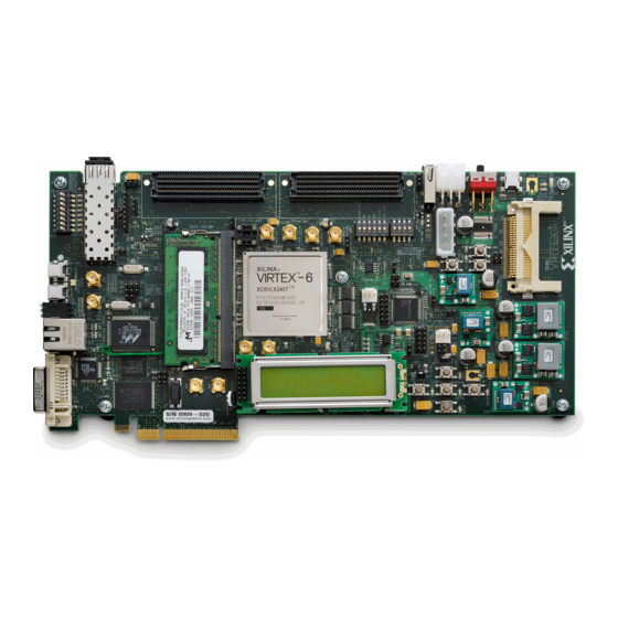
Table 1-1 the section headings in this document. X-Ref Target - Figure 1-2 (on backside) UG534_02_123009 Figure 1-2: ML605 Board Photo The numbered features in Figure 1-2 correlate to the features and notes listed in Table 1-1. - Page 12 Chapter 1: ML605 Evaluation Board Table 1-1: ML605 Features (Cont’d) Schematic Number Feature Notes Page 200 MHz OSC, oscillator socket, SMA Clock generation connectors a. 200 MHz oscillator (on Epson 200 MHz 2.5V LVDS OSC backside) b. Oscillator socket, single- MMD Components 66 MHz 2.5V...
-
Page 13: Virtex-6 Xc6Vlx240T-1Ffg1156 Fpga
Electronics SG-BGA-6046 FPGA socket. References See the Virtex-6 FPGA Data Sheet. [Ref 4] Configuration The ML605 supports configuration in the following modes: • Slave SelectMAP (using Platform Flash XL with the onboard 47 MHz oscillator) • Master BPI-Up (using Linear BPI Flash device) •... -
Page 14: I/O Voltage Rails
Chapter 1: ML605 Evaluation Board The ML605 supports Master BPI-Up, JTAG, and Slave SelectMAP. These are selected by setting M[2:0] options 010, 101 and 110 shown in Table 1-2. Table 1-2: Virtex-6 FPGA Configuration Modes Configuration Mode M[2:0] Bus Width... -
Page 15: Mb Ddr3 Memory Sodimm
2. 512 MB DDR3 Memory SODIMM A 512MB DDR3 SODIMM is provided as a flexible and efficient form-factor volatile memory for user applications. The ML605 SODIMM socket is wired to support a maximum SODIMM size of 2 GB. The ML605 DDR3 64-bit wide interface has been tested to 800 MT/s. - Page 16 Chapter 1: ML605 Evaluation Board Table 1-4: DDR3 SODIMM Connections (Cont’d) J1 SODIMM U1 FPGA Pin Schematic Net Name Pin Number Pin Name DDR3_A6 DDR3_A7 DDR3_A8 DDR3_A9 DDR3_A10 A10/AP DDR3_A11 DDR3_A12 A12_BC_N DDR3_A13 DDR3_A14 DDR3_A15 DDR3_BA0 DDR3_BA1 DDR3_BA2 DDR3_D0 DDR3_D1...
- Page 17 DDR3_D39 DQ39 DDR3_D40 DQ40 DDR3_D41 DQ41 DDR3_D42 DQ42 DDR3_D43 DQ43 DDR3_D44 DQ44 DDR3_D45 DQ45 DDR3_D46 DQ46 DDR3_D47 DQ47 DDR3_D48 DQ48 DDR3_D49 DQ49 DDR3_D50 DQ50 DDR3_D51 DQ51 DDR3_D52 DQ52 DDR3_D53 DQ53 ML605 Hardware User Guide www.xilinx.com UG534 (v1.2.1) January 21, 2010...
- Page 18 Chapter 1: ML605 Evaluation Board Table 1-4: DDR3 SODIMM Connections (Cont’d) J1 SODIMM U1 FPGA Pin Schematic Net Name Pin Number Pin Name DDR3_D54 DQ54 DDR3_D55 DQ55 DDR3_D56 DQ56 DDR3_D57 DQ57 DDR3_D58 DQ58 DDR3_D59 DQ59 DDR3_D60 DQ60 DDR3_D61 DQ61 DDR3_D62...
- Page 19 See the Micron Technology, Inc. for more information [Ref 22]. In addition, see the Virtex-6 FPGA Memory Interface Solutions User Guide [Ref 6] and the Virtex-6 FPGA Memory Resources User Guide [Ref ML605 Hardware User Guide www.xilinx.com UG534 (v1.2.1) January 21, 2010...
-
Page 20: Mb Platform Flash Xl
FPGA design recommendations. 4. 32 MB Linear BPI Flash A Numonyx JS28F256P30 Linear BPI Flash memory (P30) on the ML605 provides 32 MB of non-volatile storage that can be used for configuration as well as software storage. The Linear BPI Flash shares the dual use configuration pins in parallel with the XCF128 Platform Flash XL. -
Page 21: Ml605 Flash Boot Options
Detailed Description ML605 Flash Boot Options The ML605 has two parallel wired flash memory devices as shown in Figure 1-3. At ML605 power-up, before FPGA configuration, DIP switch S2 switch 2 selects which flash device, U4 (BPI) or U27 (Platform Flash), provides the boot bitstream. Typically S2 switch 2 will be open/OFF to select the U27 Platform Flash. - Page 22 Chapter 1: ML605 Evaluation Board Table 1-5: Platform Flash and BPI Flash Connections (Cont’d) U4 BPI Flash U27 Platform Flash U1 FPGA Pin Schematic Net Name Pin Number Pin Name Pin Number Pin Name AF24 FLASH_D0 DQ00 AF25 FLASH_D1 DQ01...
- Page 23 Resources tab for more information. Also, see the Platform Flash XL High-Density Configuration and Storage Device Data Sheet [Ref 17] and the Virtex-6 Configuration User Guide [Ref 10]. ML605 Hardware User Guide www.xilinx.com UG534 (v1.2.1) January 21, 2010...
-
Page 24: System Ace Cf And Compactflash Connector
CompactFlash, with the xilinx.sys file located in the root directory. The xilinx.sys file is used by the System ACE CF controller to define the project directory structure, which consists of one main folder containing eight sub-folders used to store the eight ACE files containing the configuration images. - Page 25 1. The System ACE CF clock is sourced from U28 32.000 MHz osc. References See the System ACE CF product page and the System ACE CompactFlash Solution Data Sheet. [Ref 18] ML605 Hardware User Guide www.xilinx.com UG534 (v1.2.1) January 21, 2010...
-
Page 26: Usb Jtag
6. USB JTAG JTAG configuration is provided through onboard USB-to-JTAG configuration logic where a computer host accesses the ML605 JTAG chain through a Type-A (computer host side) to Type-Mini-B (ML605 side) USB cable. The JTAG chain of the board is illustrated in Figure 1-4. -
Page 27: Clock Generation
7. Clock Generation There are three FPGA fabric clock sources available on the ML605 . Oscillator (Differential) The ML605 has one 2.5V LVDS differential 200 MHz oscillator (U11) soldered onto the board and wired to an FPGA global clock input. •... - Page 28 Chapter 1: ML605 Evaluation Board X-Ref Target - Figure 1-7 Silkscreened outline has beveled corner Socket has notch in crossbar UG534_07_092109 Figure 1-7: ML605 Oscillator Socket Pin 1 Location Identifiers www.xilinx.com ML605 Hardware User Guide UG534 (v1.2.1) January 21, 2010...
-
Page 29: Sma Connectors (Differential)
Oscillator top has corner dot marking UG534_08_092109 Figure 1-8: ML605 Oscillator Pin 1 Location Identifiers SMA Connectors (Differential) A high-precision clock signal can be provided to the FPGA using differential clock signals through the onboard 50-ohm SMA connectors J58(P)/J55(N). - Page 30 Chapter 1: ML605 Evaluation Board GTX SMA Clock The ML605 includes a pair of SMA connectors for a GTX (MGT) Clock as described in Figure 1-9 Table 1-7. X-Ref Target - Figure 1-9 J30 32K10K-400E3 GND1 GND2 GND3 SMA_REFCLK_C_N1 GND4...
-
Page 31: Multi-Gigabit Transceivers (Gtx Mgts)
Detailed Description 8. Multi-Gigabit Transceivers (GTX MGTs) The ML605 provides access to 20 MGTs. • Eight (8) of the MGTs are wired to the PCIe x8 Endpoint (P1) edge connector fingers • Eight (8) of the MGTs are wired to the FMC HPC connector (J64) •... -
Page 32: Pci Express Endpoint Connectivity
The ML605 board trace impedance on all PCIe lanes supports both Gen1 and Gen2 applications. The ML605 supports up to Gen1 x8 and Gen2 x4 as shipped with a -1 speed grade for the LX240T device. - Page 33 PCIE_RX4_P PETp4 Integrated Endpoint block GTXE1_X0Y10 receive pair PCIE_RX4_N PETn4 PCIE_RX5_P PETp5 Integrated Endpoint block GTXE1_X0Y9 receive pair PCIE_RX5_N PETn5 PCIE_RX6_P PETp6 Integrated Endpoint block GTXE1_X0Y8 receive pair PCIE_RX6_N PETn6 ML605 Hardware User Guide www.xilinx.com UG534 (v1.2.1) January 21, 2010...
- Page 34 AC adapter might be required. If a different AC adapter is used, its load regulation should be better than ±10%. ML605 power switch SW2 turns the board on and off by controlling the 12V supply to the board.
-
Page 35: Sfp Module Connector
Low = Module Present Jumper J54 SFP_RT_SEL Jumper Pins 1-2 = Full Bandwidth Jumper Pins 2-3 = Reduced Bandwidth Test Point J51 SFP_LOS High = Loss of Receiver Signal Low = Normal Operation ML605 Hardware User Guide www.xilinx.com UG534 (v1.2.1) January 21, 2010... -
Page 36: 100/1000 Tri-Speed Ethernet Phy
FPGA signal SFP_TX_DISABLE_FPGA. 11. 10/100/1000 Tri-Speed Ethernet PHY The ML605 utilizes the onboard Marvell Alaska PHY device (88E1111) for Ethernet communications at 10, 100, or 1000 Mb/s. The board supports MII, GMII, RGMII, and SGMII interfaces from the FPGA to the PHY (Table 1-11). -
Page 37: Sgmii Gtx Transceiver Clock Generation
PHY_INT INT_B AH13 PHY_RESET RESET_B AL13 PHY_CRS AK13 PHY_COL AP11 PHY_RXCLK RXCLK AG12 PHY_RXER RXER AM13 PHY_RXCTL_RXDV RXDV AN13 PHY_RXD0 RXD0 AF14 PHY_RXD1 RXD1 AE14 PHY_RXD2 RXD2 AN12 PHY_RXD3 RXD3 ML605 Hardware User Guide www.xilinx.com UG534 (v1.2.1) January 21, 2010... - Page 38 Chapter 1: ML605 Evaluation Board Table 1-13: Ethernet PHYConnections (Cont’d) U80 M88E1111 U1 FPGA Pin Schematic Net Name Pin Number Pin Name AM12 PHY_RXD4 RXD4 AD11 PHY_RXD5 RXD5 AC12 PHY_RXD6 RXD6 AC13 PHY_RXD7 RXD7 AH12 PHY_TXC_GTXCLK GTXCLK AD12 PHY_TXCLK TXCLK...
-
Page 39: Usb-To-Uart Bridge
The ML605 contains a Silicon Labs CP2103GM USB-to-UART bridge device (U34) which allows connection to a host computer with a USB cable. The USB cable is supplied in this evaluation kit (Type A end to host computer, Type Mini-B end to ML605 connector J21). Table 1-14 details the ML605 J21 pinout. -
Page 40: Usb Controller
Chapter 1: ML605 Evaluation Board 13. USB Controller The ML605 provides USB support via a Cypress CY7C67300 EZ-Host™ Programmable Embedded USB Host and Peripheral Controller (U81). The host port is a USB Type-A connector (J5). A USB keyboard (without an internal USB hub) will be able to connect to this USB Host port to demonstrate functionality. -
Page 41: Dvi Codec
Detailed Description 14. DVI Codec The ML605 features a DVI connector (P3) to support an external video monitor. The DVI circuitry utilizes a Chrontel CH7301C (U38) capable of 1600 X 1200 resolution with 24-bit color. The video interface chip drives both the digital and analog signals to the DVI connector. -
Page 42: Iic Bus
Chapter 1: ML605 Evaluation Board 15. IIC Bus The ML605 implements four IIC bus interfaces at the FPGA. The "MAIN" IIC bus hosts four items: • FPGA U1 Bank 34 "MAIN" IIC interface • 8Kb NV Memory U6 • FMC HPC connector J64 •... - Page 43 IIC_SDA_DVI_F 2 Kb EEPROM IIC_SDA_MAIN Addr: 0b1010000 Addr: 0b0011011 Temperature Sensor DVI CODEC SFP_MOD_DEF2 SFP MODULE CHRONTEL CONNECTOR SFP_MOD_DEF1 CH730C-TF Addr: 0b1010000 Addr: 0b1110110 UG534_14_092109 Figure 1-14: IIC Bus Topology ML605 Hardware User Guide www.xilinx.com UG534 (v1.2.1) January 21, 2010...
-
Page 44: Kb Nv Memory
Chapter 1: ML605 Evaluation Board 8 Kb NV Memory The ML605 hosts an 8 Kb ST Microelectronics M24C08-WDW6TP IIC parameter storage memory device (U6). The IIC address of U7 is 0b1010100, and U6 is not write protected (WP pin 7 is tied to GND). -
Page 45: Status Leds
DDR3 VTTDDR Power Good DS30 SYSACE_ERR_LED System ACE CF System ACE CF Error Error LED DS31 FPGA_INIT_B INIT FPGA Initialization in progress DS32 DVI_GPIO1_FMC_C2M_PG GREEN FMC PWR GD FMC Power Good ML605 Hardware User Guide www.xilinx.com UG534 (v1.2.1) January 21, 2010... -
Page 46: Ethernet Phy Status Leds
Chapter 1: ML605 Evaluation Board Ethernet PHY Status LEDs The Ethernet PHY status LEDs are mounted to be visible when the ML605 board is installed into a PC motherboard. They are mounted in right-angle, plastic housings and can be seen on the connector end of the board. This cluster of six LEDs is installed adjacent to the RJ45 Ethernet jack P2. -
Page 47: Fpga Init And Done Leds
Detailed Description FPGA INIT and DONE LEDs The typical Xilinx FPGA power up and configuration status LEDs are present on the ML605. The red INIT LED DS31 comes on momentarily after the FPGA powers up and during its internal power-on process. The DONE LED DS13 comes on after the FPGA programming bitstream has been downloaded and the FPGA successfully configured. -
Page 48: User Leds
Chapter 1: ML605 Evaluation Board User LEDs The ML605 provides two groups of active-High LEDs as described in Figure 1-18 Table 1-21. X-Ref Target - Figure 1-18 GPIO_LED_0 GPIO_LED_1 GPIO_LED_2 GPIO_LED_3 GPIO_LED_4 GPIO_LED_5 GPIO_LED_6 GPIO_LED_7 H-1X8 27.4 27.4 27.4 27.4 27.4... -
Page 49: User Pushbutton Switches
AH27 GPIO_LED_N – DS20 User Pushbutton Switches The ML605 provides six active-High pushbutton switches: • SW5, SW6, SW7, SW8 and SW9, arranged in a diamond configuration to depict “directional” headings North, South, East, West and Center respectively • SW10 CPU Reset pushbutton... -
Page 50: User Dip Switch
SW7.2 GPIO_SW_W SW8.2 GPIO_SW_C SW9.2 CPU_RESET SW10.2 User DIP Switch The ML605 includes an active-High eight pole DIP switch as described in Figure 1-20 Table 1-23. X-Ref Target - Figure 1-20 VCC1V5 GPIO DIP SW1 GPIO DIP SW2 GPIO DIP SW3... -
Page 51: User Sma Gpio
Detailed Description User SMA GPIO The ML605 includes an pair of SMA connectors for GPIO as described in Figure 1-21 Table 1-24. X-Ref Target - Figure 1-21 J56 32K10K-400E3 GND1 GND2 GND3 GND4 GND5 GND6 GND7 USER SMA GPIO N... -
Page 52: Lcd Display (16 Character X 2 Lines)
Chapter 1: ML605 Evaluation Board LCD Display (16 Character x 2 Lines) The ML605 board has a 16-character x 2-line LCD (Display Tech S162D BA BC, installed onto J41 2x7 header) on the board to display text information. Potentiometer R270 adjusts the contrast of the LCD. -
Page 53: Switches
MODE, Boot EEPROM Select and CCLK Osc Enable DIP switch S2 (active-High) Power On/Off Slide Switch SW2 SW2 is the ML605 board main power on/off switch. Sliding the switch actuator from the off to on position applies 12V power from either J60 (6-pin Mini-Fit) or J25 (4-pin ATX) Ω... -
Page 54: Fpga_Prog_B Pushbutton Sw4 (Active-Low)
Chapter 1: ML605 Evaluation Board FPGA_PROG_B Pushbutton SW4 (Active-Low) This switch grounds the FPGA's PROG_B pin when pressed. This action clears the FPGA. See the Virtex-6 FPGA Data Sheet for more information on clearing the contents of the FPGA. [Ref 4]... -
Page 55: System Ace Cf Compactflash Image Select Dip Switch S1
System ACE to boot at power-on if it finds a CF card present. In order to boot from BPI Flash U4 or Xilinx Platform Flash (U27) without System ACE contention, S1 switch 4 must be OFF. ML605 Hardware User Guide www.xilinx.com... -
Page 56: Mode, Osc Enable, Boot Eeprom Select, And Addr Select Dip Switch S2
SiT8102 (X4). When switch 1 is closed (CCLK_EXTERNAL High), X4 drives a 47 MHz clock onto the FPGA_CCLK signal. Boot EEPROM Select: S2 switch 2 is used to select the between the Xilinx Platform Flash or the Numonyx Linear BPI Flash for the FPGA boot memory device. -
Page 57: Vita 57.1 Fmc Hpc Connector
“4. 32 MB Linear BPI Flash,” page 20 details. 19. VITA 57.1 FMC HPC Connector The ML605 implements both the High Pin Count (HPC, J64) and Low Pin Count (LPC, J63) connector options of VITA 57.1.1 FMC specification. This section discusses the FMC HPC J64 connector. - Page 58 Chapter 1: ML605 Evaluation Board Note: The ML605 board VADJ voltage for the FMC HPC and LPC connectors (J64 and J63) is fixed at 2.5V (non-adjustable). The 2.5V rail cannot be turned off. The ML605 VITA 57.1 FMC interfaces are compatible with 2.5V mezzanine cards capable of supporting 2.5V VADJ.
- Page 59 FMC_HPC_HA12_N AE32 FMC_HPC_HA16_N AB33 FMC_HPC_HA15_P AB32 FMC_HPC_HA20_P FMC_HPC_HA15_N AC32 FMC_HPC_HA20_N FMC_HPC_HA19_P FMC_HPC_HB03_P AL30 FMC_HPC_HA19_N FMC_HPC_HB03_N AM31 FMC_HPC_HB02_P AP32 FMC_HPC_HB05_P AN33 FMC_HPC_HB02_N AP33 FMC_HPC_HB05_N AN34 FMC_HPC_HB04_P AM33 FMC_HPC_HB09_P AL34 FMC_HPC_HB04_N AL33 ML605 Hardware User Guide www.xilinx.com UG534 (v1.2.1) January 21, 2010...
- Page 60 Chapter 1: ML605 Evaluation Board Table 1-28: VITA 57.1 FMC HPC Connections (Cont’d) J64 FMC U1 FPGA J64 FMC U1 FPGA Schematic Net Name Schematic Net Name HPC Pin HPC Pin FMC_HPC_HB09_N AK34 FMC_HPC_HB08_P AK33 FMC_HPC_HB13_P AH33 FMC_HPC_HB08_N AK32 FMC_HPC_HB13_N...
- Page 61 2. These signals do not connect to U1 FPGA pins. The pin numbers in the right-hand column identify the device and pin these signals are connected to (U88.17 = U88 pin 17, and so on). ML605 Hardware User Guide www.xilinx.com...
- Page 62 Chapter 1: ML605 Evaluation Board Table 1-29: Power Supply Voltages for HPC Connector Allowable Max Capacitive Voltage Supply No Pins Max Amps Tolerance Voltage Range Load VADJ Fixed 2.5V +/- 5% 1000 uF VIO_B_M2C 0-VADJ 1.15 +/- 5% 500 uF...
-
Page 63: Vita 57.1 Fmc Lpc Connector
-3 dB insertion loss point within a two-level signaling environment. Note: The ML605 board VADJ voltage for the FMC HPC and LPC connectors (J64 and J63) is fixed at 2.5V (non-adjustable). The 2.5V rail cannot be turned off. The ML605 VITA 57.1 FMC interfaces are compatible with 2.5V mezzanine cards capable of supporting 2.5V VADJ. - Page 64 Chapter 1: ML605 Evaluation Board Table 1-30 shows the VITA 57.1 FMC LPC connections. The connector pinout is in Appendix B, “VITA 57.1 FMC LPC (J63) and HPC (J64) Connector Pinout.” Any signal named FMC_LPC_xxxx that is wired between a U1 FPGA pin and some other device does not appear in this table..
-
Page 65: Power Management
Mini-Fit type connector J60. The AC-to-DC power supply included in the kit has a mating 6-pin plug. When the ML605 is installed into a table top or tower PC's PCIe slot, the ML605 is typically powered from the PC ATX power supply. One of the ATX hard disk type 4-pin power connectors is plugged into ML605 connector J25. -
Page 66: Onboard Power Regulation
Chapter 1: ML605 Evaluation Board Onboard Power Regulation Figure 1-28 shows the ML605 onboard power supply architecture. The ML605 uses power solutions from Texas Instruments. X-Ref Target - Figure 1-28 Power Supply PWR Jack J25/J60 Linear Regulator TL1963 VCC5 5.0V@1.5A max... - Page 67 TI USB Interface Adapter PMBus pod and associated TI GUI. References For more detailed information about this technology and the various power management controllers and regulator modules offered by Texas Instruments, visit http://www.ti.com/ww/en/analog/digital-power/index.html. ML605 Hardware User Guide www.xilinx.com UG534 (v1.2.1) January 21, 2010...
-
Page 68: System Monitor
-40°C to +125°C is obtained using an external reference. Figure 1-29 illustrates the power supply and reference options on the ML605. For a more detailed discussion of these requirements, see the Virtex-6 FPGA System Monitor User Guide. - Page 69 Vccint_shunt_N SYSMON_VN C169 AGND SYSMON_VP 0.01UF To Measure VCCINT Current: Dedicated Analog Inputs Jumper on 9-11, 10-12 Connect Vccint shunt to Vp,Vn UG534_37 _081209 Figure 1-30: System Monitor Header (J35) ML605 Hardware User Guide www.xilinx.com UG534 (v1.2.1) January 21, 2010...
- Page 70 In addition to monitoring the FPGA core supply power consumption, two auxiliary analog input channels (of the 16 that are available) are used to implement a power monitor for the entire ML605 board. The board power is monitored at the 12V power input connector. Figure 1-31 shows how the power monitor is implemented and connected to the System Monitor auxiliary input channels 12 and 13.
- Page 71 In highly demanding situations, active thermal management in the form of a heat sink and fan may be required. In order to support this, drive circuitry for an external fan has been provided on the ML605. A fan with tach output can be connect at header J59 as shown in Figure 1-32.
- Page 72 System Monitor ML605 Demonstration Design The various features described in this section are easily evaluated using a MicroBlaze™ based reference designed provided with the ML605 Evaluation Board. This reference design supports a UART based interface using a terminal program such as Hyperterminal to provide information on the FPGA power supplies, temperature, and power consumption.
-
Page 73: Configuration Options
BPI Mode JTAG With the mode set to JTAG 101, the ML605 will not attempt to boot or load a bitstream from either of the Flash devices. If a CompactFlash (CF) card is installed in the CF socket U73, System ACE CF will attempt to load a bitstream from the CF card image address pointed to by the image select switch S1. - Page 74 Chapter 1: ML605 Evaluation Board www.xilinx.com ML605 Hardware User Guide UG534 (v1.2.1) January 21, 2010...
- Page 75 1. S1 position 4 is the System ACE controller enable switch. When ON, this switch allows the System ACE to boot at power on if it finds a CF card present. In order to boot from BPI Flash or Xilinx Platform Flash without System ACE contention, S1 switch 4 must be OFF.
- Page 76 R-kelvin on 12V rail Jump 10 - 12 SFP Module: Full BW Jump 1 - 2 SFP Enable Jump 1 - 2 PCIe Lane Size: 1 lane Jump 1 - 2 www.xilinx.com ML605 Hardware User Guide UG534 (v1.2.1) January 21, 2010...
-
Page 77: Connector Pinout
G A1 12P0V G ND LA33_P 3P 3V LA32_P LA33_N 12P0V LA32_N 3P3V G ND G ND VADJ 3P3V V ADJ G ND 3P 3V Figure B-1: FMC LPC Connector Pinout ML605 Hardware User Guide www.xilinx.com UG534 (v1.2.1) January 21, 2010... - Page 78 Appendix B: VITA 57.1 FMC LPC (J63) and HPC (J64) Connector Pinout Figure B-2 shows the pinout of the FMC HPC connector. X-Ref Target - Figure B-2 Figure B-2: FMC HPC Connector Pinout www.xilinx.com ML605 Hardware User Guide UG534 (v1.2.1) January 21, 2010...
- Page 79 Appendix C ML605 Master UCF The UCF template is provided for designs that target the ML605. Net names provided in the constraints below correlate with net names on the ML605 Rev. D schematic. On identifying the appropriate pins, the net names below should be replaced with net names in the user RTL.
- Page 80 Appendix C: ML605 Master UCF NET "DDR3_D8" LOC = "M13"; ## 21 on J1 NET "DDR3_D9" LOC = "J14"; ## 23 on J1 NET "DDR3_D10" LOC = "B13"; ## 33 on J1 NET "DDR3_D11" LOC = "B12"; ## 35 on J1 NET "DDR3_D12"...
- Page 81 ## 17 on U4, B7 on U27 NET "FLASH_A19" LOC = "AN9"; ## 16 on U4, C7 on U27 NET "FLASH_A20" LOC = "AF10"; ## 11 on U4, C8 on U27 ML605 Hardware User Guide www.xilinx.com UG534 (v1.2.1) January 21, 2010...
- Page 82 Appendix C: ML605 Master UCF NET "FLASH_A21" LOC = "AF9"; ## 10 on U4, A8 on U27 NET "FLASH_A22" LOC = "AL9"; ## 9 on U4, G1 on U27 NET "FLASH_A23" LOC = "AA23"; ## 26 on U4 NET "FLASH_D0"...
- Page 83 ## J24 on J64 NET "FMC_HPC_HB02_N" LOC = "AP33"; ## F23 on J64 NET "FMC_HPC_HB02_P" LOC = "AP32"; ## F22 on J64 NET "FMC_HPC_HB03_N" LOC = "AM31"; ## E22 on J64 ML605 Hardware User Guide www.xilinx.com UG534 (v1.2.1) January 21, 2010...
- Page 84 Appendix C: ML605 Master UCF NET "FMC_HPC_HB03_P" LOC = "AL30"; ## E21 on J64 NET "FMC_HPC_HB04_N" LOC = "AL33"; ## F26 on J64 NET "FMC_HPC_HB04_P" LOC = "AM33"; ## F25 on J64 NET "FMC_HPC_HB05_N" LOC = "AN34"; ## E25 on J64 NET "FMC_HPC_HB05_P"...
- Page 85 ## D12 on J63 NET "FMC_LPC_LA05_P" LOC = "H34"; ## D11 on J63 NET "FMC_LPC_LA06_N" LOC = "J34"; ## C11 on J63 NET "FMC_LPC_LA06_P" LOC = "K33"; ## C10 on J63 ML605 Hardware User Guide www.xilinx.com UG534 (v1.2.1) January 21, 2010...
- Page 86 Appendix C: ML605 Master UCF NET "FMC_LPC_LA07_N" LOC = "H32"; ## H14 on J63 NET "FMC_LPC_LA07_P" LOC = "G32"; ## H13 on J63 NET "FMC_LPC_LA08_N" LOC = "K29"; ## G13 on J63 NET "FMC_LPC_LA08_P" LOC = "J30"; ## G12 on J63 NET "FMC_LPC_LA09_N"...
- Page 87 ## B15 on P1 NET "PCIE_RX0_P" LOC = "J3"; ## B14 on P1 NET "PCIE_RX1_N" LOC = "K6"; ## B20 on P1 NET "PCIE_RX1_P" LOC = "K5"; ## B19 on P1 ML605 Hardware User Guide www.xilinx.com UG534 (v1.2.1) January 21, 2010...
- Page 88 Appendix C: ML605 Master UCF NET "PCIE_RX2_N" LOC = "L4"; ## B24 on P1 NET "PCIE_RX2_P" LOC = "L3"; ## B23 on P1 NET "PCIE_RX3_N" LOC = "N4"; ## B28 on P1 NET "PCIE_RX3_P" LOC = "N3"; ## B27 on P1 NET "PCIE_RX4_N"...
- Page 89 ## 6 on U31 NET "USB_D3_LS" LOC = "T31"; ## 16 on U31 NET "USB_D4_LS" LOC = "T29"; ## 4 on U31 NET "USB_D5_LS" LOC = "V28"; ## 18 on U31 ML605 Hardware User Guide www.xilinx.com UG534 (v1.2.1) January 21, 2010...
- Page 90 Appendix C: ML605 Master UCF NET "USB_D6_LS" LOC = "V27"; ## 2 on U31 NET "USB_D7_LS" LOC = "U25"; ## 12 on U30 NET "USB_D8_LS" LOC = "Y28"; ## 14 on U29 NET "USB_D9_LS" LOC = "W32"; ## 8 on U29 NET "USB_D10_LS"...
- Page 91 IP. For additional information, see www.xilinx.com/support/documentation/index.htm. Documents supporting the ML605 Evaluation Board: UG535, ML605 Reference Design User Guide UG525, Getting Started with the Xilinx Virtex-6 FPGA ML605 Evaluation Kit DS150, Virtex-6 Family Overview DS152, Viretx-6 FPGA Data Sheet: DC and Switching Characteristics...
- Page 92 Components, MBH Series Data Sheet (MBH2100H-66.000 MHz) SIG, PCI Express Specifications 28. Marvell, Alaska Gigabit Ethernet Transceivers Product Page Cypress Semiconductor, CY7C67300 Data Sheet USB Implementers Forum, Inc., USB Specifications Micro, M24C08 Data Sheet Samtec, Inc. www.xilinx.com ML605 Hardware User Guide UG534 (v1.2.1) January 21, 2010...
Need help?
Do you have a question about the ML605 and is the answer not in the manual?
Questions and answers