Xilinx KC705 User Manual
For the kintex-7 fpga
Hide thumbs
Also See for KC705:
- User manual (118 pages) ,
- Getting started (24 pages) ,
- User manual (90 pages)

Related Manuals for Xilinx KC705


Summary of Contents for Xilinx KC705
- Page 1 KC705 Evaluation Board for the Kintex-7 FPGA User Guide UG810 (v1.6.2) August 26, 2015...
-
Page 2: Revision History
(including loss of data, profits, goodwill, or any type of loss or damage suffered as a result of any action brought by a third party) even if such damage or loss was reasonably foreseeable or Xilinx had been advised of the possibility of the same. - Page 3 Appendix C, Master Constraints File Listing, changed appendix title from Master UCF Listing to Master Board Constraints, replaced references to the term UCF with the term XDC and replaced the KC705 Board UCF Listing with the KC705 Board XDC Listing.
- Page 4 KC705 Evaluation Board www.xilinx.com UG810 (v1.6.2) August 26, 2015...
-
Page 5: Table Of Contents
KC705 Board Features ........ - Page 6 ..............110 www.xilinx.com KC705 Evaluation Board Send Feedback...
-
Page 7: Chapter 1: Kc705 Evaluation Board Features
Chapter 1 KC705 Evaluation Board Features Overview The KC705 evaluation board for the Kintex®-7 FPGA provides a hardware environment for developing and evaluating designs targeting the Kintex-7 XC7K325T-2FFG900C FPGA. The KC705 board provides features common to many embedded processing systems, including a DDR3 SODIMM memory, an 8-lane PCI Express®... - Page 8 Chapter 1: KC705 Evaluation Board Features • Ethernet PHY SGMII interface (RJ-45 connector) • PCI Express endpoint connectivity • Gen1 8-lane (x8) • Gen2 8-lane (x8) • SFP+ Connector • 10/100/1000 tri-speed Ethernet PHY • USB-to-UART bridge • High-Definition Multimedia Interface ™ (HDMI) technology codec •...
-
Page 9: Feature Descriptions
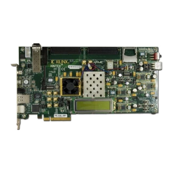
Kintex-7 FPGA KC705 Evaluation Kit website. Caution! The KC705 board can be damaged by electrostatic discharge (ESD). Follow standard ESD prevention measures when handling the board X-Ref Target - Figure 1-1 1 GB DDR3 Memory... - Page 10 Chapter 1: KC705 Evaluation Board Features X-Ref Target - Figure 1-2 Round callout references a component Square callout references a component on the front side of the board on the back side of the board User rotary switch located under LCD...
-
Page 11: Kintex-7 Fpga
For further information on Kintex-7 FPGAs, see 7 Series FPGAs Overview (DS180) [Ref FPGA Configuration The KC705 board supports three of the five 7 series FPGA configuration modes: • Master SPI flash memory using the onboard Quad SPI flash memory •... - Page 12 For full details on configuring the FPGA, see 7 Series FPGAs Configuration User Guide (UG470) [Ref Encryption Key Backup Circuit FPGA U1 implements bitstream encryption key technology. The KC705 board provides the encryption key backup battery circuit shown in Figure 1-4. The rechargeable 1.5V lithium button-type battery B1 is soldered to the board with the positive output connected to FPGA U1 VCCBATT pin C10.
- Page 13 Figure 1-4: Encryption Key Backup Circuit I/O Voltage Rails There are 10 I/O banks available on the Kintex-7 device. The voltages applied to the FPGA I/O banks used by the KC705 board are listed in Table 1-3. Table 1-3: I/O Voltage Rails...
-
Page 14: Ddr3 Memory Module
Chapter 1: KC705 Evaluation Board Features DDR3 Memory Module [Figure 1-2, callout 2] The memory module at J1 is a 1 GB DDR3 small outline dual-inline memory module (SODIMM). It provides volatile synchronous dynamic random access memory (SDRAM) for storing user code and data. - Page 15 SSTL15 DQ25 AG15 DDR3_D26 SSTL15 DQ26 AF15 DDR3_D27 SSTL15 DQ27 AH17 DDR3_D28 SSTL15 DQ28 AG14 DDR3_D29 SSTL15 DQ29 AH15 DDR3_D30 SSTL15 DQ30 AK15 DDR3_D31 SSTL15 DQ31 DDR3_D32 SSTL15 DQ32 KC705 Evaluation Board www.xilinx.com Send Feedback UG810 (v1.6.2) August 26, 2015...
- Page 16 Chapter 1: KC705 Evaluation Board Features Table 1-4: DDR3 Memory Connections to the FPGA (Cont’d) J1 DDR3 Memory U1 FPGA Pin Net Name I/O Standard Pin Number Pin Name DDR3_D33 SSTL15 DQ33 DDR3_D34 SSTL15 DQ34 DDR3_D35 SSTL15 DQ35 DDR3_D36 SSTL15...
- Page 17 DQS7_P DDR3_ODT0 SSTL15 ODT0 AC10 DDR3_ODT1 SSTL15 ODT1 DDR3_RESET_B LVCMOS15 RESET_B AC12 DDR3_S0_B SSTL15 S0_B DDR3_S1_B SSTL15 S1_B DDR3_TEMP_E SSTL15 EVENT_B VENT DDR3_WE_B SSTL15 WE_B AC11 DDR3_CAS_B SSTL15 CAS_B KC705 Evaluation Board www.xilinx.com Send Feedback UG810 (v1.6.2) August 26, 2015...
-
Page 18: Linear Bpi Flash Memory
AE11 DDR3_CLK1_P DIFF_SSTL15 CK1_P The KC705 DDR3 SODIMM interface adheres to the constraints guidelines documented in the DDR3 Design Guidelines section of 7 Series FPGAs Memory Interface Solutions User Guide (UG586) [Ref 3]. The KC705 DDR3 SODIMM interface is a 40Ω impedance implementation. - Page 19 LVCMOS25 FLASH_A18 LVCMOS25 FLASH_A19 LVCMOS25 FLASH_A20 LVCMOS25 FLASH_A21 LVCMOS25 FLASH_A22 LVCMOS25 FLASH_A23 LVCMOS25 FLASH_A24 LVCMOS25 FLASH_A25 LVCMOS25 FLASH_D0 LVCMOS25 FLASH_D1 LVCMOS25 FLASH_D2 LVCMOS25 FLASH_D3 LVCMOS25 FLASH_D4 LVCMOS25 FLASH_D5 LVCMOS25 KC705 Evaluation Board www.xilinx.com Send Feedback UG810 (v1.6.2) August 26, 2015...
- Page 20 2]. The configuration section in this document provides details on the Master BPI configuration mode. Figure 1-5 shows the connections of the linear BPI flash memory on the KC705 board. For more information about the Micron PC28F00AP30TF part, see [Ref www.xilinx.com...
-
Page 21: Quad Spi Flash Memory
• Part number: N25Q128A13BSF40F (Micron) • Supply voltage: 2.8V • Datapath width: 4 bits • Data rate: Various depending on Single/Dual/Quad mode and CCLK rate KC705 Evaluation Board www.xilinx.com Send Feedback UG810 (v1.6.2) August 26, 2015... - Page 22 [Ref 2] provides details on using the Quad SPI flash memory. Figure 1-6 shows the connections of the Quad SPI flash memory on the KC705 board. For more information about the Micron N25Q128A13BSF40F part, see [Ref X-Ref Target - Figure 1-6...
-
Page 23: Sd Card Interface
[Figure 1-2, callout 5] The KC705 board includes a secure digital input/output (SDIO) interface to provide user-logic access to general purpose nonvolatile SDIO memory cards and peripherals. The SD card slot is designed to support 50 MHz high speed SD cards. -
Page 24: Usb Jtag Module
UG810_c1_08_031214 Figure 1-8: JTAG Chain Block Diagram When an FMC card is attached to the KC705 board, it is automatically added to the JTAG chain through electronically controlled single-pole single-throw (SPST) switches U76 and U77. The SPST switches are in a normally closed state and transition to an open state when an FMC mezzanine card is attached. - Page 25 FPGA using the Xilinx software. In addition, the JTAG connector allows debug tools or a software debugger to access the FPGA. The Xilinx software tool can also indirectly program the Linear BPI or the Quad SPI flash memory. To accomplish this, the software configures the FPGA with a temporary design to access and program the BPI or Quad SPI flash memory device.
-
Page 26: Clock Generation
Chapter 1: KC705 Evaluation Board Features Clock Generation There are five clock sources available for the FPGA fabric on the KC705 board (refer to Table 1-8). Table 1-8: KC705 Board Clock Sources Clock Name Reference Description System Clock SiT9102 2.5V LVDS 200 MHz Fixed Frequency Oscillator (Si Time). - Page 27 [Figure 1-2, callout 7] The KC705 board has a 2.5V LVDS differential 200 MHz oscillator (U6) soldered onto the back side of the board and wired to an FPGA MRCC clock input on bank 33. This 200 MHz signal pair is named SYSCLK_P and SYSCLK_N, which are connected to FPGA U1 pins AD12 and AD11 respectively.
- Page 28 [Ref 9] • XTP187, KC705 Si570 Fixed Frequencies [Ref 10] • RDF0176, KC705 Si570 Fixed Frequencies Design Files [Ref 11] User SMA Clock Input [Figure 1-2, callout 9] An external high-precision clock signal can be provided to the FPGA bank 15 by connecting differential clock signals through the onboard 50Ω...
- Page 29 [Figure 1-2, callout 10] The KC705 board includes a pair of SMA connectors for a GTX clock wired to GTX Quad bank 117. This differential clock has signal names SMA_MGT_REFCLK_P and SMA_REFCLK_N, which are connected to FPGA U1 pins J8 and J7 respectively.
- Page 30 Chapter 1: KC705 Evaluation Board Features The Silicon Labs Si5324 U70 pin 1 reset net SI5326_RST must be driven High to enable the device. U70 pin 1 net SI5326_RST is level-shifted to VADJ by U75 and is connected to U1 bank 12 pin AE20.
-
Page 31: Gtx Transceivers
The GTX transceivers in 7 series FPGAs are grouped into four channels described as Quads. The reference clock for a Quad can be sourced from the Quad above or Quad below the GTX Quad of interest. There are four GTX Quads on the KC705 board with connectivity as shown here: •... - Page 32 Chapter 1: KC705 Evaluation Board Features Table 1-10 lists the GTX interface connections to the FPGA (U1). Table 1-10: GTX Interface Connections for FPGA U1 Transceiver Bank Associated Net Name Connections MGT_BANK_115 GTXE2_CHANNEL_X0Y0 PCIe7 GTXE2_CHANNEL_X0Y1 PCIe6 GTXE2_CHANNEL_X0Y2 PCIe5 GTXE2_CHANNEL_X0Y3 PCIe4...
-
Page 33: Pci Express Edge Connector
100Ω differential pair. The 7 series FPGAs GTX transceivers are used for multi-gigabit per second serial interfaces. The XC7K325T-2FFG900C FPGA (-2 speed grade) included with the KC705 board supports up to Gen2 x8. The PCIe clock is input from the edge connector. It is AC coupled to the FPGA through the MGTREFCLK1 pins of Quad 115. - Page 34 Chapter 1: KC705 Evaluation Board Features Table 1-11: PCIe Edge Connector Connections (Cont’d) Schematic FPGA Pin PCIe Edge PCIe Edge Pin FFG900 Function Net Name (U1) Connector Pin Name Placement PCIE_RX3_N PETn3 Integrated Endpoint block receive pair GTXE2_CHANNEL_X0Y4 PCIE_RX4_P PETp4...
- Page 35 PCIE_RX4_P PETp4 GTXE2_CHANNEL_X0Y3 MGTXRXN3_115_V5 PCIE_RX4_N PETn4 GTXE2_CHANNEL_X0Y3 MGTREFCLK0P_115_R8 MGT_BANK_115 MGTREFCLK0N_115_R7 MGT_BANK_115 MGTREFCLK1P_115_U8 PCIE_CLK_QO_P REFCLK+ MGT_BANK_115 MGTREFCLK1N_115_U7 PCIE_CLK_QO_N REFCLK- MGT_BANK_115 MGTAVTTRCAL_115_W7 MGTAVTT MGT_BANK_115 MGTRREF_115_W8 100 ohm P/U to MGTAVTT MGT_BANK_115 KC705 Evaluation Board www.xilinx.com Send Feedback UG810 (v1.6.2) August 26, 2015...
- Page 36 Chapter 1: KC705 Evaluation Board Features Table 1-13 lists the PCIe edge connector connections for Quad 116. Table 1-13: GTX Quad 116 to PCIe Edge Connector Connections Quad 116 FPGA Pin Schematic PCIe Edge PCIe Edge FFG900 Pin Name (U1)
-
Page 37: Sfp/Sfp+ Connector
Feature Descriptions SFP/SFP+ Connector [Figure 1-2, callout 14] The KC705 board contains a small form-factor pluggable (SFP+) connector and cage assembly that accepts SFP or SFP+ modules. Figure 1-17 shows the SFP+ module connector circuitry. X-Ref Target - Figure 1-17... - Page 38 TX_DISABLE Notes: 1. On KC705 boards prior to Rev 1.1, SFP+ connector P5 pin 18 RD_P is connected to net SFP_RX_N, and pin 19 RD_N is connected to net SFP_RX_P. 2. On KC705 boards prior to Rev 1.1, SFP+ connector P5 pin 18 TD_P is connected to net SFP_TX_N, and pin 19 TD_N is connected to net SFP_TX_P.
-
Page 39: 10/100/1000 Tri-Speed Ethernet Phy
10/100/1000 Tri-Speed Ethernet PHY [Figure 1-2, callout 15] The KC705 board utilizes the Marvell Alaska PHY device (88E1111) U37 for Ethernet communications at 10, 100, or 1000 Mb/s. The board supports MII, GMII, RGMII, and SGMII interfaces from the FPGA to the PHY (Table 1-16). - Page 40 Chapter 1: KC705 Evaluation Board Features SGMII GTX Transceiver Clock Generator [Figure 1-2, callout 16] An Integrated Circuit Systems ICS844021I chip (U2) generates a high-quality, low-jitter, 125 MHz LVDS clock from a 25 MHz crystal (X3). This clock is sent to FPGA U1, bank 117 GTX transceiver (clock pins G8 (P) and G7 (N)) driving the SGMII interface.
-
Page 41: Usb-To-Uart Bridge
USB cable is plugged into the USB port on the KC705 board. Xilinx UART IP is expected to be implemented in the FPGA fabric. The FPGA supports the USB-to-UART bridge using four signal pins: Transmit (TX), Receive (RX), Request to Send (RTS), and Clear to Send (CTS). -
Page 42: Hdmi Video Output
[Figure 1-2, callout 18] The KC705 board provides a High-Definition Multimedia Interface (HDMI) video output using the Analog Devices ADV7511KSTZ-P HDMI transmitter (U65). The HDMI output is provided on a Molex 500254-1927 HDMI type-A connector (P6). The ADV7511 is wired to support 1080P 60Hz, YCbCr 4:2:2 encoding via 16-bit input data mapping. - Page 43 DSD4 DSD5 DSD_CLK MCLK GND1 GND2 GND3 I2S0 GND4 I2S1 GND5 I2S2 GND6 I2S3 GND7 SCLK GND8 LRCLK GND9 GND10 R_EXT GND11 R433 UG810_c1_19_031214 Figure 1-19: HDMI Codec Circuit KC705 Evaluation Board www.xilinx.com Send Feedback UG810 (v1.6.2) August 26, 2015...
- Page 44 Chapter 1: KC705 Evaluation Board Features Table 1-21 lists the connections between the codec and the FPGA. Table 1-21: FPGA to HDMI Codec Connections (ADV7511) ADV7511 (U65) U1 FPGA Pin Schematic Net Name I/O Standard Pin Number Pin Name HDMI_D0...
-
Page 45: Lcd Character Display
For more information about the ADV7511KSTZ-P part, see [Ref 17]. LCD Character Display [Figure 1-2, callout 19] A 2-line by 16-character display is provided on the KC705 board (Figure 1-20). X-Ref Target - Figure 1-20 LCD Display (16 x 2) UG810_c1_20_031214... - Page 46 UG810_c1_21_031214 Figure 1-21: LCD Interface Circuit The KC705 board base board uses a male Samtec MTLW-107-07-G-D-265 2x7 header (J31) with 0.025-inch square posts on 0.100-inch centers for connecting to a Samtec SLW-107-01-L-D female socket on the LCD display panel assembly. The LCD header...
-
Page 47: I2C Bus Switch
18]. I2C Bus Switch [Figure 1-2, callout 20] The KC705 board implements a single I C port on the FPGA (IIC_SDA_MAIN, IIC_SDA_SCL), which is routed through a TI PCA9548 1-to-8 channel I C switch (U49). U49 pin 24 net IIC_MUX_RESET_B is connected to U1 bank 15 pin P23. This is an... -
Page 48: Status Leds
Chapter 1: KC705 Evaluation Board Features Table 1-24 lists the address for each device on the I C bus. Table 1-24: I C Devices C Switch C Device C Address Position Si570 Clock 0b1011101 FMC HPC 0bXXXXX00 FMC LPC 0bXXXXX00... -
Page 49: Ethernet Phy Status Leds
The Ethernet PHY status LEDs are mounted to be visible through the metal bracket on the left edge of the KC705 board when it is installed into a PCIe slot in a PC chassis. The six PHY status LEDs are located above the RJ45 Ethernet jack as shown in Figure 1-24. - Page 50 Chapter 1: KC705 Evaluation Board Features • User Rotary Switch (callout 25, hidden beneath the LCD) • ROTARY_PUSH, ROTARY_INCA, ROTARY_INCB: SW8 • User SMA (callout 26) • USER_SMA_GPIO_P, USER_SMA_GPIO_N: J13, J14 • 2 line x 16 character LCD Character Display (callout 19) •...
- Page 51 CPU Reset Pushbutton [Figure 1-2, callout 37] Figure 1-27 shows the CPU reset pushbutton circuit. X-Ref Target - Figure 1-27 VCC1V5 CPU_RESET 4.7kΩ 0.1 W UG810_c1_27_031214 Figure 1-27: CPU Reset Pushbutton KC705 Evaluation Board www.xilinx.com Send Feedback UG810 (v1.6.2) August 26, 2015...
- Page 52 Chapter 1: KC705 Evaluation Board Features GPIO DIP Switch [Figure 1-2, callout 24] Figure 1-28 shows the GPIO DIP Switch circuit. X-Ref Target - Figure 1-28 SW11 VADJ GPIO_DIP_SW3 GPIO_DIP_SW2 GPIO_DIP_SW1 GPIO_DIP_SW0 SDA04H1SBD 4.7kΩ 4.7kΩ 0.1 W 0.1 W 4.7kΩ...
- Page 53 GPIO_LED_4 LVCMOS25 DS3.2 GPIO_LED_5 LVCMOS25 DS25.2 GPIO_LED_6 LVCMOS25 DS26.2 GPIO_LED_7 LVCMOS25 DS27.2 Directional Pushbutton Switches AA12 GPIO_SW_N LVCMOS15 SW2.1 GPIO_SW_E LVCMOS15 SW3.1 AB12 GPIO_SW_S LVCMOS15 SW4.1 GPIO_SW_W LVCMOS15 SW6.1 KC705 Evaluation Board www.xilinx.com Send Feedback UG810 (v1.6.2) August 26, 2015...
-
Page 54: Switches
[Figure 1-2, callout 27] The KC705 board power switch is SW15. Sliding the switch actuator from the Off to On position applies 12V power from J49, a 6-pin mini-fit connector. Green LED DS22 illuminates when the KC705 board power is on. See... - Page 55 Figure 1-32 for powering the KC705 board from the ATX power supply 4-pin peripheral connector. The Xilinx part number for this cable is 2600304, and is equivalent to Sourcegate Technologies part number AZCBL-WH-1109-RA4. For information on ordering this cable, see [Ref 20].
-
Page 56: Fpga Mezzanine Card Interface
1-2, callout - 31] The KC705 evaluation board for the Kintex-7 FPGA supports the VITA 57.1 FPGA Mezzanine Card (FMC) specification by providing subset implementations of a high pin count (HPC) connector at J22 and a low pin count (LPC) connector at J2. Both connectors use the same 10 x 40 form factor, except the HPC version is fully populated with 400 pins and the LPC version is partially populated with 160 pins. - Page 57 The HPC signals are distributed across GTX Quads 116, 117, and 118. Each of these Quads have their VCCO voltage connected to VADJ. Note: The KC705 board VADJ voltage for the J22 and J2 connectors is determined by the FMC VADJ power sequencing logic described in Power Management, page...
- Page 58 Chapter 1: KC705 Evaluation Board Features Table 1-28: HPC Connections, J22 to FPGA U1 (Cont’d) FPGA FPGA J22 Pin Schematic Net Name J22 Pin Schematic Net Name Standard U1 Pin Standard U1 Pin FMC_HPC_GBTCLK1_M2C_P LVDS FMC_HPC_DP1_C2M_P FMC_HPC_GBTCLK1_M2C_N LVDS FMC_HPC_DP1_C2M_N FMC_HPC_DP2_C2M_P...
- Page 59 LVDS FMC_HPC_HA08_P LVDS FMC_HPC_HA13_P LVDS FMC_HPC_HA08_N LVDS FMC_HPC_HA13_N LVDS FMC_HPC_HA12_P LVDS FMC_HPC_HA16_P LVDS FMC_HPC_HA12_N LVDS FMC_HPC_HA16_N LVDS FMC_HPC_HA15_P LVDS FMC_HPC_HA20_P LVDS FMC_HPC_HA15_N LVDS FMC_HPC_HA20_N LVDS FMC_HPC_HA19_P LVDS FMC_HPC_HA19_N LVDS KC705 Evaluation Board www.xilinx.com Send Feedback UG810 (v1.6.2) August 26, 2015...
- Page 60 Chapter 1: KC705 Evaluation Board Features Table 1-28: HPC Connections, J22 to FPGA U1 (Cont’d) FPGA FPGA J22 Pin Schematic Net Name J22 Pin Schematic Net Name Standard U1 Pin Standard U1 Pin VADJ VADJ FMC_HPC_CLK1_M2C_P LVDS LVCMO FMC_HPC_CLK1_M2C_N LVDS...
- Page 61 LVDS FMC_HPC_HA10_P LVDS FMC_HPC_HA14_P LVDS FMC_HPC_HA10_N LVDS FMC_HPC_HA14_N LVDS FMC_HPC_HA17_CC_P LVDS FMC_HPC_HA18_P LVDS FMC_HPC_HA17_CC_N LVDS FMC_HPC_HA18_N LVDS FMC_HPC_HA21_P LVDS FMC_HPC_HA22_P LVDS FMC_HPC_HA21_N LVDS FMC_HPC_HA22_N LVDS FMC_HPC_HA23_P LVDS FMC_HPC_HA23_N LVDS KC705 Evaluation Board www.xilinx.com Send Feedback UG810 (v1.6.2) August 26, 2015...
- Page 62 Chapter 1: KC705 Evaluation Board Features LPC Connector J2 [Figure 1-2, callout 31] The 160-pin LPC connector defined by the FMC specification (Figure B-2, page provides connectivity for up to: • 68 single-ended or 34 differential user-defined signals • 1 GTX transceiver •...
- Page 63 LVDS AK28 FMC_LPC_LA19_N LVDS AK26 FMC_LPC_LA25_P LVDS AC26 FMC_LPC_LA21_P LVDS AG27 FMC_LPC_LA25_N LVDS AD26 FMC_LPC_LA21_N LVDS AG28 FMC_LPC_LA29_P LVDS AE28 FMC_LPC_LA24_P LVDS AG30 FMC_LPC_LA29_N LVDS AF28 FMC_LPC_LA24_N LVDS AH30 KC705 Evaluation Board www.xilinx.com Send Feedback UG810 (v1.6.2) August 26, 2015...
-
Page 64: Power Management
[Figure 1-2, callout 32] The KC705 board uses power regulators and PMBus compliant digital PWM system controllers from Texas Instruments to supply core and auxiliary voltages. The Texas Instruments Fusion Digital Power graphical user interface (GUI) is used to monitor the current and temperature levels of the board power modules. - Page 65 Feature Descriptions The KC705 board power distribution diagram is shown in Figure 1-35. X-Ref Target - Figure 1-35 VCC12_P Power Plane Power Controller 1 (Core) From SW15 U55 Address 52 VCCINT Switching Regulator 1.0V at 20A VCCAUX Switching Regulator 1.8V at 20A...
- Page 66 Chapter 1: KC705 Evaluation Board Features The KC705 board core and auxiliary voltages are listed in Table 1-30. Table 1-30: Onboard Power System Devices Reference Power Rail Net Power Rail Schematic Device Type Description Designator Name Voltage Page Core voltage controller and regulators...
- Page 67 1-33. FMC_VADJ Voltage Control The FMC_VADJ rail is set to 2.5V. When the KC705 board is powered on, the state of the FMC_VADJ_ON_B signal wired to header J65 is sampled by the Texas Instruments UCD9248 controller U55. If a jumper is installed on J65, signal FMC_VADJ_ON_B is held low, and the TI controller U55 energizes the FMC_VADJ rail at power on.
- Page 68 Chapter 1: KC705 Evaluation Board Features X-Ref Target - Figure 1-36 VCC12_P R392 R393 10.0K 1% 10.0K 1% 1/10W 1/10W SM_FAN_TACH FPGA Fan Tach U1 Pin U22 Cooling Fan +12V R390 2.7V 4.75K 1% Fan GND 500 mW 100V 1/10W...
- Page 69 1.38 10.41 Notes: 1. The values defined in these columns are the voltage, current, and temperature thresholds that cause the regulator to shut down if the value is exceeded. KC705 Evaluation Board www.xilinx.com Send Feedback UG810 (v1.6.2) August 26, 2015...
-
Page 70: Xadc Header
Chapter 1: KC705 Evaluation Board Features Table 1-33 defines the voltage and current values for each power rail controlled by the UCD9248 PMBus controller at Address 54 (U89). Table 1-33: Power Rail Specifications for UCD9248 PMBus controller at Address 54... - Page 71 UG810_c1_37_031214 Figure 1-37: Header XADC_VREF Voltage Source Options The KC705 board supports both the internal FPGA sensor measurements and the external measurement capabilities of the XADC. Internal measurements of the die temperature, VCCINT, VCCAUX, and VCCBRAM are available. The KC705 board VCCINT and VCCBRAM are provided by a common 1.0 V supply.
- Page 72 Chapter 1: KC705 Evaluation Board Features X-Ref Target - Figure 1-38 XADC_VN XADC_VP XADC_VAUX0P XADC_VAUX0N XADC_VCC5V0 XADC_VAUX8N XADC_VAUX8P XADC_DXP VADJ XADC_VREF XADC_DXN XADC_VCC_HEADER XADC_GPIO_1 XADC_GPIO_0 XADC_GPIO_2 XADC_GPIO_3 XADC_AGND XADC_AGND UG810_c1_38_031214 Figure 1-38: XADC Header (J46) Table 1-34 describes the XADC header J46 pin functions.
-
Page 73: Configuration Options
Configuration Options Configuration Options The FPGA on the KC705 board can be configured by the following methods: • Master BPI (uses the Linear BPI flash memory) • Master SPI (uses the Quad SPI flash memory) • JTAG (uses the USB-to-JTAG Bridge or Download cable). See... - Page 74 Chapter 1: KC705 Evaluation Board Features To obtain the fastest configuration speed an external 66 MHz oscillator is wired to the EMCCLK pin of the FPGA. This allows users to create bitstreams that configure the FPGA over the 16-bit datapath from the Linear BPI flash memory at a maximum synchronous read rate of 33 MHz.
-
Page 75: Appendix A: Default Switch And Jumper Settings
Table A-2. X-Ref Target - Figure A-2 ON Position = 1 2 3 4 5 OFF Position = 0 UG810_aA_02_031214 Figure A-2: SW13 Default Settings KC705 Evaluation Board www.xilinx.com Send Feedback UG810 (v1.6.2) August 26, 2015... -
Page 76: Default Jumper Settings
Default FLASH_A25 FLASH_A24 FPGA_M2 FPGA_M1 FPGA_M0 Default Jumper Settings Figure A-3 for the locations of jumpers listed in Table A-3. Table A-3: KC705 Default Jumper Settings Header Jumper Schematic Callout Reference Description Position 0381502 Page Designator 2-pin SPI SELECT = Onboard SPI flash memory device... - Page 77 Default Jumper Settings X-Ref Target - Figure A-3 UG810_aA_03_111414 Figure A-3: KC705 Jumper Locations KC705 Evaluation Board www.xilinx.com Send Feedback UG810 (v1.6.2) August 26, 2015...
- Page 78 Appendix A: Default Switch and Jumper Settings www.xilinx.com KC705 Evaluation Board Send Feedback UG810 (v1.6.2) August 26, 2015...
-
Page 79: Appendix B: Vita 57.1 Fmc Connector Pinouts
Figure B-1 shows the pinout of the FPGA Mezzanine Card (FMC) high pin count (HPC) connector defined by the VITA 57.1 FMC specification. For a description of how the KC705 board implements the FMC specification, see FPGA Mezzanine Card Interface, page 56... - Page 80 Figure B-2 shows the pinout of the FMC card low pin count (LPC) connector defined by the VITA 57.1 FMC specification. For a description of how the KC705 board implements the FMC specification, see FPGA Mezzanine Card Interface, page 56...
-
Page 81: Appendix C: Master Constraints File Listing
Kintex-7 KC705 Evaluation Kit product page Doc & Designs tab for the latest versions of the FPGA pins constraints files (XDC files). Choose the Xilinx tools link. In the search box, search for KC705 Master XDC File. KC705 Board XDC Listing... - Page 82 IOSTANDARD SSTL15 [get_ports DDR3_D18] set_property PACKAGE_PIN AF18 [get_ports DDR3_D19] set_property IOSTANDARD SSTL15 [get_ports DDR3_D19] set_property PACKAGE_PIN AH19 [get_ports DDR3_D20] set_property IOSTANDARD SSTL15 [get_ports DDR3_D20] set_property PACKAGE_PIN AJ19 [get_ports DDR3_D21] www.xilinx.com KC705 Evaluation Board Send Feedback UG810 (v1.6.2) August 26, 2015...
- Page 83 KC705 Board XDC Listing set_property IOSTANDARD SSTL15 [get_ports DDR3_D21] set_property PACKAGE_PIN AE19 [get_ports DDR3_D22] set_property IOSTANDARD SSTL15 [get_ports DDR3_D22] set_property PACKAGE_PIN AD19 [get_ports DDR3_D23] set_property IOSTANDARD SSTL15 [get_ports DDR3_D23] set_property PACKAGE_PIN AK16 [get_ports DDR3_D24] set_property IOSTANDARD SSTL15 [get_ports DDR3_D24] set_property PACKAGE_PIN AJ17 [get_ports DDR3_D25]...
- Page 84 IOSTANDARD SSTL15 [get_ports DDR3_A12] set_property PACKAGE_PIN AH11 [get_ports DDR3_A13] set_property IOSTANDARD SSTL15 [get_ports DDR3_A13] set_property PACKAGE_PIN AK10 [get_ports DDR3_A14] set_property IOSTANDARD SSTL15 [get_ports DDR3_A14] set_property PACKAGE_PIN AK11 [get_ports DDR3_A15] www.xilinx.com KC705 Evaluation Board Send Feedback UG810 (v1.6.2) August 26, 2015...
- Page 85 KC705 Board XDC Listing set_property IOSTANDARD SSTL15 [get_ports DDR3_A15] set_property PACKAGE_PIN AH9 [get_ports DDR3_BA0] set_property IOSTANDARD SSTL15 [get_ports DDR3_BA0] set_property PACKAGE_PIN AG9 [get_ports DDR3_BA1] set_property IOSTANDARD SSTL15 [get_ports DDR3_BA1] set_property PACKAGE_PIN AK9 [get_ports DDR3_BA2] set_property IOSTANDARD SSTL15 [get_ports DDR3_BA2] #CLK...
- Page 86 PACKAGE_PIN T23 [get_ports FLASH_D7] set_property IOSTANDARD LVCMOS25 [get_ports FLASH_D7] set_property PACKAGE_PIN U20 [get_ports FLASH_D8] set_property IOSTANDARD LVCMOS25 [get_ports FLASH_D8] set_property PACKAGE_PIN P29 [get_ports FLASH_D9] set_property IOSTANDARD LVCMOS25 [get_ports FLASH_D9] www.xilinx.com KC705 Evaluation Board Send Feedback UG810 (v1.6.2) August 26, 2015...
- Page 87 KC705 Board XDC Listing set_property PACKAGE_PIN R29 [get_ports FLASH_D10] set_property IOSTANDARD LVCMOS25 [get_ports FLASH_D10] set_property PACKAGE_PIN P27 [get_ports FLASH_D11] set_property IOSTANDARD LVCMOS25 [get_ports FLASH_D11] set_property PACKAGE_PIN P28 [get_ports FLASH_D12] set_property IOSTANDARD LVCMOS25 [get_ports FLASH_D12] set_property PACKAGE_PIN T30 [get_ports FLASH_D13] set_property IOSTANDARD LVCMOS25 [get_ports FLASH_D13]...
- Page 88 PACKAGE_PIN D5 [get_ports FMC_HPC_DP1_M2C_N] set_property PACKAGE_PIN D6 [get_ports FMC_HPC_DP1_M2C_P] set_property PACKAGE_PIN B1 [get_ports FMC_HPC_DP2_C2M_N] set_property PACKAGE_PIN B2 [get_ports FMC_HPC_DP2_C2M_P] set_property PACKAGE_PIN B5 [get_ports FMC_HPC_DP2_M2C_N] set_property PACKAGE_PIN B6 [get_ports FMC_HPC_DP2_M2C_P] www.xilinx.com KC705 Evaluation Board Send Feedback UG810 (v1.6.2) August 26, 2015...
- Page 89 KC705 Board XDC Listing set_property PACKAGE_PIN A3 [get_ports FMC_HPC_DP3_C2M_N] set_property PACKAGE_PIN A4 [get_ports FMC_HPC_DP3_C2M_P] set_property PACKAGE_PIN A7 [get_ports FMC_HPC_DP3_M2C_N] set_property PACKAGE_PIN A8 [get_ports FMC_HPC_DP3_M2C_P] #FMC HPC LA set_property PACKAGE_PIN B25 [get_ports FMC_HPC_LA00_CC_N] set_property IOSTANDARD LVCMOS25 [get_ports FMC_HPC_LA00_CC_N] set_property PACKAGE_PIN C25 [get_ports FMC_HPC_LA00_CC_P]...
- Page 90 PACKAGE_PIN B18 [get_ports FMC_HPC_LA26_P] set_property IOSTANDARD LVCMOS25 [get_ports FMC_HPC_LA26_P] set_property PACKAGE_PIN B19 [get_ports FMC_HPC_LA27_N] set_property IOSTANDARD LVCMOS25 [get_ports FMC_HPC_LA27_N] set_property PACKAGE_PIN C19 [get_ports FMC_HPC_LA27_P] set_property IOSTANDARD LVCMOS25 [get_ports FMC_HPC_LA27_P] www.xilinx.com KC705 Evaluation Board Send Feedback UG810 (v1.6.2) August 26, 2015...
- Page 91 KC705 Board XDC Listing set_property PACKAGE_PIN C16 [get_ports FMC_HPC_LA28_N] set_property IOSTANDARD LVCMOS25 [get_ports FMC_HPC_LA28_N] set_property PACKAGE_PIN D16 [get_ports FMC_HPC_LA28_P] set_property IOSTANDARD LVCMOS25 [get_ports FMC_HPC_LA28_P] set_property PACKAGE_PIN B17 [get_ports FMC_HPC_LA29_N] set_property IOSTANDARD LVCMOS25 [get_ports FMC_HPC_LA29_N] set_property PACKAGE_PIN C17 [get_ports FMC_HPC_LA29_P] set_property IOSTANDARD LVCMOS25 [get_ports FMC_HPC_LA29_P]...
- Page 92 PACKAGE_PIN J11 [get_ports FMC_HPC_HA21_P] set_property IOSTANDARD LVCMOS25 [get_ports FMC_HPC_HA21_P] set_property PACKAGE_PIN K11 [get_ports FMC_HPC_HA22_N] set_property IOSTANDARD LVCMOS25 [get_ports FMC_HPC_HA22_N] set_property PACKAGE_PIN L11 [get_ports FMC_HPC_HA22_P] set_property IOSTANDARD LVCMOS25 [get_ports FMC_HPC_HA22_P] www.xilinx.com KC705 Evaluation Board Send Feedback UG810 (v1.6.2) August 26, 2015...
- Page 93 KC705 Board XDC Listing set_property PACKAGE_PIN L13 [get_ports FMC_HPC_HA23_N] set_property IOSTANDARD LVCMOS25 [get_ports FMC_HPC_HA23_N] set_property PACKAGE_PIN L12 [get_ports FMC_HPC_HA23_P] set_property IOSTANDARD LVCMOS25 [get_ports FMC_HPC_HA23_P] #FMC LPC MISC set_property PACKAGE_PIN J22 [get_ports FMC_LPC_PRSNT_M2C_B_LS] set_property IOSTANDARD LVCMOS25 [get_ports FMC_LPC_PRSNT_M2C_B_LS] #FMC LPC CLK...
- Page 94 PACKAGE_PIN AF26 [get_ports FMC_LPC_LA20_P] set_property IOSTANDARD LVCMOS25 [get_ports FMC_LPC_LA20_P] set_property PACKAGE_PIN AG28 [get_ports FMC_LPC_LA21_N] set_property IOSTANDARD LVCMOS25 [get_ports FMC_LPC_LA21_N] set_property PACKAGE_PIN AG27 [get_ports FMC_LPC_LA21_P] set_property IOSTANDARD LVCMOS25 [get_ports FMC_LPC_LA21_P] www.xilinx.com KC705 Evaluation Board Send Feedback UG810 (v1.6.2) August 26, 2015...
- Page 95 KC705 Board XDC Listing set_property PACKAGE_PIN AK28 [get_ports FMC_LPC_LA22_N] set_property IOSTANDARD LVCMOS25 [get_ports FMC_LPC_LA22_N] set_property PACKAGE_PIN AJ27 [get_ports FMC_LPC_LA22_P] set_property IOSTANDARD LVCMOS25 [get_ports FMC_LPC_LA22_P] set_property PACKAGE_PIN AH27 [get_ports FMC_LPC_LA23_N] set_property IOSTANDARD LVCMOS25 [get_ports FMC_LPC_LA23_N] set_property PACKAGE_PIN AH26 [get_ports FMC_LPC_LA23_P] set_property IOSTANDARD LVCMOS25 [get_ports FMC_LPC_LA23_P]...
- Page 96 IOSTANDARD LVCMOS15 [get_ports LCD_E_LS] set_property PACKAGE_PIN Y11 [get_ports LCD_RS_LS] set_property IOSTANDARD LVCMOS15 [get_ports LCD_RS_LS] set_property PACKAGE_PIN AB13 [get_ports LCD_RW_LS] set_property IOSTANDARD LVCMOS15 [get_ports LCD_RW_LS] #GPIO USER SMA set_property PACKAGE_PIN Y24 [get_ports USER_SMA_GPIO_N] www.xilinx.com KC705 Evaluation Board Send Feedback UG810 (v1.6.2) August 26, 2015...
- Page 97 KC705 Board XDC Listing set_property IOSTANDARD LVCMOS25 [get_ports USER_SMA_GPIO_N] set_property PACKAGE_PIN Y23 [get_ports USER_SMA_GPIO_P] set_property IOSTANDARD LVCMOS25 [get_ports USER_SMA_GPIO_P] #SMA MGT RX/TX set_property PACKAGE_PIN K5 [get_ports SMA_MGT_RX_N] set_property PACKAGE_PIN K6 [get_ports SMA_MGT_RX_P] set_property PACKAGE_PIN K1 [get_ports SMA_MGT_TX_N] set_property PACKAGE_PIN K2 [get_ports SMA_MGT_TX_P]...
- Page 98 IOSTANDARD LVCMOS25 [get_ports PHY_RXCLK] set_property PACKAGE_PIN U30 [get_ports PHY_RXD0] set_property IOSTANDARD LVCMOS25 [get_ports PHY_RXD0] set_property PACKAGE_PIN U25 [get_ports PHY_RXD1] set_property IOSTANDARD LVCMOS25 [get_ports PHY_RXD1] set_property PACKAGE_PIN T25 [get_ports PHY_RXD2] www.xilinx.com KC705 Evaluation Board Send Feedback UG810 (v1.6.2) August 26, 2015...
- Page 99 KC705 Board XDC Listing set_property IOSTANDARD LVCMOS25 [get_ports PHY_RXD2] set_property PACKAGE_PIN U28 [get_ports PHY_RXD3] set_property IOSTANDARD LVCMOS25 [get_ports PHY_RXD3] set_property PACKAGE_PIN R19 [get_ports PHY_RXD4] set_property IOSTANDARD LVCMOS25 [get_ports PHY_RXD4] set_property PACKAGE_PIN T27 [get_ports PHY_RXD5] set_property IOSTANDARD LVCMOS25 [get_ports PHY_RXD5] set_property PACKAGE_PIN T26 [get_ports PHY_RXD6]...
- Page 100 IOSTANDARD LVCMOS25 [get_ports USB_TX] Note: Regarding USB UART—The XDC constraints for pins K24 and M19 do not match those in the Vivado part0_pins.xml file. See Kintex-7 KC705 FGPA Evaluation Kit Master Answer Record (AR 45934) for more information. #XADC...
- Page 101 KC705 Board XDC Listing set_property PACKAGE_PIN AA25 [get_ports XADC_GPIO_1] set_property IOSTANDARD LVCMOS25 [get_ports XADC_GPIO_1] set_property PACKAGE_PIN AB28 [get_ports XADC_GPIO_2] set_property IOSTANDARD LVCMOS25 [get_ports XADC_GPIO_2] set_property PACKAGE_PIN AA27 [get_ports XADC_GPIO_3] set_property IOSTANDARD LVCMOS25 [get_ports XADC_GPIO_3] set_property PACKAGE_PIN J24 [get_ports XADC_VAUX0N_R] set_property IOSTANDARD LVCMOS25 [get_ports XADC_VAUX0N_R]...
- Page 102 Appendix C: Master Constraints File Listing www.xilinx.com KC705 Evaluation Board Send Feedback UG810 (v1.6.2) August 26, 2015...
-
Page 103: Appendix D: Board Setup
Connect the ATX power supply to the KC705 board using the ATX power supply adapter cable as shown in Figure D-1: Plug the 6-pin 2 x 3 Molex connector on the adapter cable into J49 on the KC705 board. KC705 Evaluation Board www.xilinx.com Send Feedback UG810 (v1.6.2) August 26, 2015... - Page 104 Plug the 4-pin 1 x 4 peripheral power connector from the ATX power supply into the 4-pin adapter cable connector. Slide the KC705 board power switch SW12 to the ON position. The PC can now be powered on. www.xilinx.com...
-
Page 105: Appendix E: Board Specifications
Board Specifications Dimensions Height 5.5 in (14.0 cm) Length 10.5 in (26.7 cm) Note: The KC705 board height exceeds the standard 4.376 in (11.15 cm) height of a PCI Express card. Environmental Temperature Operating: 0°C to +45°C Storage: –25°C to +60°C... - Page 106 Appendix E: Board Specifications www.xilinx.com KC705 Evaluation Board Send Feedback UG810 (v1.6.2) August 26, 2015...
-
Page 107: Appendix F: Additional Resources
Topics include design assistance, advisories, and troubleshooting tips. References The most up to date information related to the KC705 board and its documentation is available on these websites: Kintex-7 KC705 FPGA KC705 Evaluation Kit... - Page 108 Aries Ang, aries.ang@sourcegate.net, +65 6483 2878 for price and availability. Note: The Xilinx ATX cable part number 2600304 is manufactured by Sourcegate Technologies and is equivalent to the Sourcegate Technologies part number AZCBL-WH-11009. Sourcegate only manufactures the latest revision, which is currently A4. This is a custom cable and cannot be ordered from the Sourcegate website.
-
Page 109: Appendix G: Regulatory And Compliance Information
Refer to the master answer record concerning the CE requirements for the PC Test Environment available at www.xilinx.com/support/answers/45934.htm Declaration of Conformity Kintex-7 FPGA KC705 Declaration of Conformity is online. Directives 2006/95/EC, Low Voltage Directive (LVD) 2004/108/EC, Electromagnetic Compatibility (EMC) Directive... -
Page 110: Markings
This product complies with Directive 2002/95/EC on the restriction of hazardous substances (RoHS) in electrical and electronic equipment. This product complies with CE Directives 2006/95/EC, Low Voltage Directive (LVD) and 2004/108/EC, Electromagnetic Compatibility (EMC) Directive. www.xilinx.com KC705 Evaluation Board Send Feedback UG810 (v1.6.2) August 26, 2015...