
Related Manuals for Motorola CPIP5430


Summary of Contents for Motorola CPIP5430
- Page 1 CPIP5430 Single Board Computer and Transition Module Installation and Use CPIP5430A/IH2 June 2004 Edition...
- Page 2 All rights reserved. Printed in the United States of America. Motorola and the stylized M logo are trademarks of Motorola, Inc., registered in the U.S. Patent and Trademark Office. All other product or service names mentioned in this document are the property of their respective owners.
- Page 3 The safety precautions listed below represent warnings of certain dangers of which Motorola is aware. You, as the user of the product, should follow these warnings and all other safety precautions necessary for the safe operation of the equipment in your operating environment.
- Page 4 Flammability All Motorola PWBs (printed wiring boards) are manufactured with a flammability rating of 94V-0 by UL-recognized manufacturers. EMI Caution This equipment generates, uses and can radiate electromagnetic energy. It Caution may cause or be susceptible to electromagnetic interference (EMI) if not installed and used with adequate EMI protection.
- Page 5 Electronic versions of this material may be read online, downloaded for personal use, or referenced in another document as a URL to the Motorola Computer Group Web site. The text itself may not be published commercially in print or electronic form, edited, translated, or otherwise altered without the permission of Motorola, Inc.
-
Page 7: Table Of Contents
PCI Mezzanine Card Installation ..............1-13 Before You Install a Board ................1-15 Installing a Board .................... 1-15 CPIP5430 Hot Swap Module Removal ............1-18 CHAPTER 2 Startup and Operation Applying Power to the System ................. 2-1 Indicators ........................2-1 LEDs for Gigabit Ethernet Port ................ - Page 8 CHAPTER 3 BIOS CPIP5430 BIOS Overview ..................3-1 Boot Menu ......................3-3 BIOS Setup Utility ....................3-5 System Summary ...................... 3-6 System Configuration Summary Screen ............3-6 System Summary Descriptions ................. 3-7 System Setup ..................... 3-8 Date / Time Descriptions ................... 3-9 BIOS Options Descriptions ................
- Page 9 Watchdog Timer (SIO Chip) ..................4-6 IPMI Controller ....................... 4-7 PCI Arbitration ......................4-7 PCI Bus 1 ......................4-8 CHAPTER 5 Rear Transition Module for CPIP5430 Features ........................5-1 Block Diagram ......................5-2 Functional Descriptions ................... 5-3 Gigabit Ethernet Interface ................. 5-3 Serial Port COM2 .....................
- Page 10 IPMB Address Map ....................C-4 PCI Interrupt Connections ..................C-5 Sensor Data Record ....................C-6 APPENDIX D IPMI Commands Introduction ......................D-1 SDR (Sensor Data Record) Device Commands ..........D-1 APPENDIX E Related Documentation Motorola Computer Group Documents ..............E-1 Related Specifications ....................E-1...
- Page 11 List of Figures Figure 1-1. CPIP5430 Layout without Heat Sink ........... 1-6 Figure 4-1. CPIP5430 Block Diagram ..............4-4 Figure 5-1. CPIP5430-RTM1 Block Diagram ............5-2 Figure 5-2. CPIP5430-RTM1 Layout ..............5-6 Figure 5-3. Serial ATA Connection Pin Assignment ..........5-19 Figure B-1.
- Page 13 Table 6-11. 10/100/1000Mb/s J16 Connector Pin Assignments ......6-15 Table 6-12. IDE Port J18 Connector Pin Assignments ......... 6-16 Table A-1. CPIP5430 Environmental Specifications ..........A-1 Table A-2. CPIP5430 SBC and RTM Power Requirements ........A-2 Table B-1. Thermally Significant Components ............B-2 Table C-1. CPIP5430 Memory Maps ..............C-1 Table C-2.
- Page 14 Table C-3. SMBUS Address Map ................C-3 Table C-4. CompactPCI Peripheral Address Map ..........C-4 Table C-5. PCI Interrupt Connections ..............C-5 Table C-6. Sensor Data Record List ............... C-6 Table E-1. Related Documents ................E-1 Table E-2. Related Specifications ................E-1...
- Page 15 CPIP5430 board and the CPIP5430-RTM01 rear transition module. It provides specific preparation and installation information, and data applicable to the board. As of the printing date of this manual, the CPIP5430 supports the models listed below. Model Number Description CPIP5430-2131-K Intel Pentium 4 CPU, 2.16 I/O, 1.7GHz, 1GB (2x512MB) memory...
-
Page 16: Summary Of Changes
MXP series chassis. Chapter 2, Startup and Operation, provides the power-up procedure, identifies the switches and indicators, and explains how to generate a soft reset on the CPIP5430. Chapter 3, BIOS, provides a description of the BIOS on the CPIP5430. -
Page 17: Comments And Suggestions
CPIP5430 single-board computer and CPIP5430- RTM01. Appendix A, Specifications, provides environmental and mechanical specifications, as well as power requirements for the CPIP5430. Appendix B, Thermal Validation, provides information to conduct thermal evaluations and identifies thermally significant components along with their maximum allowable operating temperatures. -
Page 18: Conventions Used In This Manual
In all your correspondence, please list your name, position, and company. Be sure to include the title and part number of the manual and tell how you used it. Then tell us your feelings about its strengths and weaknesses and any recommendations for improvements. -
Page 19: Description
1Hardware Preparation and Installation Description The CPIP5430 is a high performance, hot swappable peripheral slot board. It complies with PICMG 2.1, 2.9, and 2.16 specifications for 6U single slot form factor modules. Major features include: Intel Pentium Mobile P4 processor family, Intel 875P chipset with 6300 ESB, up to 4GB PC2100, dual Gigabit Ethernet interfaces for payload, separate Gigabit Ethernet interface for management, dual PMC sites, optional 2.5 inch hard drive, up... -
Page 20: Equipment Required
Hardware Preparation and Installation Equipment Required A typical CPIP5430 environment requires the following additional equipment: System enclosure, or available PICMG 2.16 slot in a system VGA monitor, VGA PMC, and USB keyboard, or serial terminal Operating system (may only require a kernel) -
Page 21: Unpacking Guidelines
Avoid touching areas of integrated circuitry; static discharge can damage circuits. Caution Motorola strongly recommends that you use an antistatic wrist strap and a Use ESD conductive foam pad when installing or upgrading a system. Electronic components, such as disk drives, computer boards, and memory modules can be extremely sensitive to electrostatic discharge (ESD). -
Page 22: Hardware Preparation
J3 connections are to a switched Ethernet fabric and pass-through connections to a rear transition module. Also, J3 and J5 provide power from the CPIP5430 to the rear transition module. It is your responsibility to verify this system compatibility. -
Page 23: Table 1-2. Cpip5430 Connectors And Headers
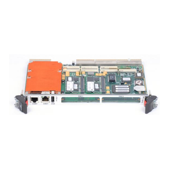
Hardware Preparation Most options on the CPIP5430 are software configurable. Configuration changes are made by setting bits in control registers after the board is installed in a system. Figure 1-1 illustrates the placement of the jumpers, headers, connectors, and various other components on the CPIP5430. Connectors and configurable headers are listed in the following table. -
Page 24: Figure 1-1. Cpip5430 Layout Without Heat Sink
Hardware Preparation and Installation Table 1-2. CPIP5430 Connectors and Headers (continued) Reference Designator Description PCI mezzanine connector, 64-pin PCI mezzanine connector, 64-pin Ethernet signal header, 4-pin 12V power for RTM USB control 4263 0304 Figure 1-1. CPIP5430 Layout without Heat Sink... -
Page 25: Hot Swap Considerations
Hot Swap Considerations Hot Swap Considerations The CPIP5430 is a CompactPCI form factor single board computer with hot swap capabilities. This allows insertion or removal of the board from a powered chassis without damage, with proper pin staging on the backplane. -
Page 26: Hardware Installation
Hardware Installation The following sections discuss the installation of memory modules, hard drives, and mezzanine cards on the CPIP5430 base board, the installation of the complete assembly into a chassis, and the system considerations relevant to installation. Before installing the CPIP5430, make sure that the serial ports and all jumpers are properly configured. -
Page 27: Jumpering Diagram For Header E1
[3-4] jumper on USB control Memory Module Installation The CPIP5430 depends upon a proprietary memory module and specialized signal routing to obtain densities of 2GB per SODIMM socket. All standard DDR SODIMM modules are compatible, however, 2GB is only achievable with the purchase of a special memory module. - Page 28 The CPIP5430 has been tested with 128MB, 256MB, 512MB, 1GB, and 2GB registered, ECC SODIMM modules. To install the memory module, follow these steps. 1. Remove the CPIP5430 from the chassis and place it on a static free surface. Note The following illustration may not represent the exact board you are using, it is meant for illustration purposes only.
-
Page 29: 2.5-Inch Hdd Installation
PMC, if not already installed from the factory. The following procedure describes how to mount a 2.5 inch hard disk drive on one of the PMC sites of the CPIP5430. If the CPIP5430 is currently installed in a system chassis, perform the following steps. - Page 30 Hardware Preparation and Installation 4. Carefully remove the CPIP5430 from its slot and lay it flat, with connectors J1 through J5 facing you. 5. Remove the PMC key-bolts of the second PMC slot. 4276 0404 6. Bolt the carrier rails onto the sides of the 2.5" HDD. The flange on each rail should be facing away from the drive.
-
Page 31: Pci Mezzanine Card Installation
(such as hard drive/controller modules); removing the key DOES NOT CHANGE the bus voltage. To install a PMC on a CPIP5430 that is currently installed in a chassis, refer to the figure on page 1-14 and perform the following steps. - Page 32 CPIP5430 and tighten the screws. 4277 0404 9. Reinstall the CPIP5430 in its proper slot. Be sure the module is well seated in the backplane connectors. 10. If necessary, connect the system to its AC or DC power source and turn the power on.
-
Page 33: Before You Install A Board
Before You Install a Board The rear I/O routing is unique and only compatible with the RTM for the CPIP5430 SBC. If you mount the HDD on the main board, the HDD will occupy the second PMC slot connector. Refer to 2.5-inch... - Page 34 Hardware Preparation and Installation Card cage rail guide description for MXP: Switch Slot = Red AMC Slots = Tan Payload Slots = Black Insert the board by holding the ejector lever—do not exert unnecessary Caution pressure on the faceplate. Caution You can remove hot-swap modules without removing the system's power.
- Page 35 Installing a Board 3. Ensure that the two handles are in the outward position.The CPIP5430 ejector handle is a Rittal Type IV (C) and has a red tab or button on the lever. Push the red button and press the ejector lever outward.
-
Page 36: Cpip5430 Hot Swap Module Removal
Hardware Preparation and Installation CPIP5430 Hot Swap Module Removal Depending on your system configuration, you may need to manually shut down software on your module prior to removal to prevent data corruption. If system software exists to do so, shutdown may occur automatically after Step 2 is performed. -
Page 37: Applying Power To The System
(if your power supply is not autosensing). When you power-on the chassis or insert the board, the CPIP5430 displays the BIOS banner and then runs a memory test. Indicators There are three LEDs and one reset switch on the front panel of the CPIP5430. -
Page 38: Hot-Swap Led
PCI bridge before implementing the reset function. The BIOS preserves as much of the system memory state as possible. PXE Boot Use the following steps to boot the CPIP5430 from a PreBoot Execution Environment (PXE) server. Note This explanation is only the sequence to get you into the PXE server environment. - Page 39 Port 0 connects to switch 1 and port 1 connects to switch 2 9. Save changes and exit Setup. the board will reboot. Once the board completes POST it will boot to the PXE server. When the boot is successful the PXE server menu will appear on the screen. http://www.motorola.com/computer/literature...
-
Page 41: Cpip5430 Bios Overview
3BIOS This chapter provides a description of the BIOS on the CPIP5430. BIOS Setup Utility System Summary System Setup Hard Disk Setup Boot Order Peripherals USB Configuration Misc Configuration Event Logging Security/Virus Exit CPIP5430 BIOS Overview The CPIP5430 BIOS software supports all of the IBM /AT standard functions and several board-specific functions and features. - Page 42 BIOS configured, the compressed portions of the BIOS are decompressed into RAM to allow the remainder of the BIOS tasks to be executed very quickly. The BIOS can now scan for and initialize other interfaces such as I/O devices and items on the PCI or ISA busses. If a video adapter is in the system it is located and initialized.
-
Page 43: Boot Menu
F1 ignores the errors and continues with the boot process. The F2 or s key can be pressed to enter the BIOS SETUP and possibly resolve any configuration error that may have been made. Press F2 or s to Run SETUP Press F1 to load default values and continue http://www.motorola.com/computer/literature... - Page 44 BIOS If the F2 key was not pressed and no errors were detected, the SYSTEM SUMMARY SCREEN is displayed (if enabled). After 10 seconds or upon pressing a key, the BIOS attempts to boot the installed operating system. The System BIOS is compatible with the Plug-and-Play Specification Version 1.0A.
-
Page 45: Bios Setup Utility
USB CONFIG Configures USB devices MISC CONFIG Configures PCI, Plug n Play, and power options EVENT LOGGING Configures the system event log SECURITY/VIRUS Configures BIOS passwords and anti-virus options EXIT Exits ROM utilities, with options to save or discard changes http://www.motorola.com/computer/literature... -
Page 46: System Summary
Memory Mode : 266 MHz Single Channel with ECC EVENT LOGGING PMC Mode : PCI 66 MHz USB Devices : None SECURITY/VIRUS ↑ ↓ Select Screen Enter Go to Sub Screen EXIT General Help Exit Motorola CPIP5430 BIOS v1.00 Beta-M Computer Group Literature Center Web Site... -
Page 47: System Summary Descriptions
Displays the PCI mode that the PMC slots are currently operating in. USB Device Displays the USB devices detected by the BIOS. Under some circumstances, such as legacy USB support being set to POST-Only, some USB devices might not be displayed. http://www.motorola.com/computer/literature... -
Page 48: System Setup
SETUP Prompt During Post Enabled Bootup Num-Lock EVENT LOGGING SYSTEM OPTIONS SECURITY/VIRUS CPU Speed Fast MPS Revision EXIT Spread Spectrum ↑ ↓ Select Screen Enter Go to Sub Screen General Help Exit Motorola CPIP5430 BIOS v1.00 Beta-M Computer Group Literature Center Web Site... -
Page 49: Date / Time Descriptions
This option determines whether the POST will pause and wait for user input when an error occurs. Prompt During Post When this option is enabled, the prompt that displays the key needed to enter SETUP will be displayed during the POST. http://www.motorola.com/computer/literature... -
Page 50: Keyboard Options Descriptions
BIOS Keyboard Options Descriptions Bootup Num-Lock Specifies the state of the Num-Lock key to be set when the system boots. System Options Descriptions CPU Speed Selects the CPU speed. This option applies only to processors that support SpeedStep technology. Processors that do not support SpeedStep will run at their rated speed. -
Page 51: Hard Disk Setup
Not Detected BOOT ORDER SECONDARY MASTER Not Detected PERIPHERALS SECONDARY SLAVE Not Detected USB CONFIG MISC. CONFIG EVENT LOGGING ↑ ↓ Select Screen Enter Go to Sub Screen SECURITY/VIRUS General Help Exit EXIT Motorola CPIP5430 BIOS v1.00 Beta-M http://www.motorola.com/computer/literature 3-11... -
Page 52: Ide Configuration Utility
↑ ↓/+- Select Screen Change Option General Help Exit Motorola CPIP5430 BIOS v1.00 Beta-M IDE Configuration Descriptions IDE Configuration Selects the configuration for the onboard parallel and serial IDE controllers. Combined Mode Selects which IDE connectors are active. When set to P-ATA Primary, the... -
Page 53: Primary Master Configuration Summary
LBA/LARGE MODE Auto Block(Multi-Sector Transfer)Mode Auto PIO MODE Auto DMA MODE Auto S.M.A.R.T. Auto 32-Bit Data Transfer Disabled ARMD Emulation Type Auto ↑ ↓ Select Screen EnterGo to Sub Screen General Help Exit Motorola CPIP5430 BIOS v1.00 Beta-M http://www.motorola.com/computer/literature 3-13... -
Page 54: Hard Drive Setup Descriptions
BIOS Hard Drive Setup Descriptions The configuration options described below work identically for HARD DRIVES 0 - 3. Device Displays the type of IDE device currently installed. Type choices include Not Installed, Hard Disk, ATAPI CDROM, and ARMD. Vendor Displays the manufacturer device identification information. Size Displays the storage capacity of the device. -
Page 55: Boot Order
Hard Disk Drives 1st Drive Ultra D0 IC25N020AT MISC. CONFIG Removable Devices EVENT LOGGING 1st Drive MITSUMI USB FDD ↑ ↓ Select Screen Enter Go to Sub Screen SECURITY/VIRUS General Help Exit EXIT Motorola CPIP5430 BIOS v1.00 Beta-M http://www.motorola.com/computer/literature 3-15... -
Page 56: Boot Order Descriptions
BIOS Boot Order Descriptions Boot Device Priority Selects the boot order for installed boot devices. The BIOS attempts to boot from items at the top of the list first. Removable Devices Boot from legacy floppy diskette, removable LS-120, or ZIP drives. -
Page 57: Peripherals
Go to Sub Screen EXIT General Help Exit Motorola CPIP5430 BIOS v1.00 Beta-M Note If you change the CSA gigabit port from the disabled state to an enabled state, you must power cycle the board after the change is made. -
Page 58: Peripherals Descriptions
BIOS Peripherals Descriptions Single CSA Gigabit This item controls the onboard 82547 CSA gigabit chip. (See Note for the Peripheral Configuration Utility on page 3-17.) CSA Gigabit Boot ROM Controls the boot ROM allowing for remote network booting with the 82547. Dual PCI-X Gigabit This item controls the onboard 82546 PCI-X gigabit chip. -
Page 59: Console Redirection Descriptions
Otherwise, software handshaking should be selected. Redirection After Control if console redirection is to be used after POST. BIOS Post Terminal Type Selects between ANSI and VT100 terminal types. VT-UTF8 Combo Controls VT-UTF8 combination key support for ANSI and VT100 Key Support terminals. http://www.motorola.com/computer/literature 3-19... -
Page 60: Usb Configuration
20 Sec USB CONFIG MISC. CONFIG No USB Mass Storage device detected EVENT LOGGING SECURITY/VIRUS ↑ ↓ Select Screen Enter Go to Sub Screen EXIT General Help Exit Motorola CPIP5430 BIOS v1.00 Beta-M 3-20 Computer Group Literature Center Web Site... -
Page 61: Usb Control Descriptions
USB Mass Storage Number of seconds to wait for a USB mass storage device after sending the Reset Delay start unit command. Emulation Type Specifies the method used to determine the type of USB mass storage devices connected. http://www.motorola.com/computer/literature 3-21... -
Page 62: Misc Configuration
ACPI APIC Support Enabled MISC. CONFIG Headless Mode Disabled ACPI Console Redirection Disabled EVENT LOGGING ↑ ↓ Select Screen Enter Go to Sub Screen SECURITY/VIRUS General Help Exit EXIT Motorola CPIP5430 BIOS v1.00 Beta-M 3-22 Computer Group Literature Center Web Site... -
Page 63: Pci Options Descriptions
Even when set to disabled, a PnP operating system may be used. Reset Configuration Data If set to “Yes”, the PnP configuration is reset after leaving SETUP and reconfigured on the next boot. This option is automatically reset to No after rebooting. http://www.motorola.com/computer/literature 3-23... -
Page 64: Acpi Options Descriptions
BIOS ACPI Options Descriptions ACPI 2.0 Support If this item is enabled, the BIOS builds the ACPI tables to comply with the ACPI 2.0 specification. When disabled, the BIOS is ACPI 1.0b compliant. ACPI APIC Support Enables or disables the ACPI support for the APIC. When enabled, a pointer to the APIC table is integrated into the RSDT pointer list. -
Page 65: Event Logging
Go to Sub Screen SECURITY/VIRUS General Help Exit EXIT Motorola CPIP5430 BIOS v1.00 Beta-M Event Logging Descriptions View Event Log This item is used to open a window containing a list of the currently logged system events. Mark All Events As Read This item is used the mark all system events in the log as read. -
Page 66: Security/Virus
Clear User Password USB CONFIG Boot Sector Virus Protection Disabled MISC. CONFIG EVENT LOGGING SECURITY/VIRUS ↑ ↓ Select Screen Enter Go to Sub Screen General Help Exit EXIT Motorola CPIP5430 BIOS v1.00 Beta-M 3-26 Computer Group Literature Center Web Site... -
Page 67: Security/Virus Descriptions
This item allows setting the user password. Clear User Password This item is used to clear the user password. Boot Sector Virus Protection When this item is enabled, a warning message is displayed before any program tries to access the boot sector. http://www.motorola.com/computer/literature 3-27... -
Page 68: Exit
BOOT ORDER Discard Changes PERIPHERALS Save Custom Defaults USB CONFIG MISC. CONFIG EVENT LOGGING ↑ ↓ Select Screen Enter Go to Sub Screen General Help Exit SECURITY/VIRUS EXIT Motorola CPIP5430 BIOS v1.00 Beta-M 3-28 Computer Group Literature Center Web Site... -
Page 69: Exit Descriptions
NVRAM. Load Custom Defaults Loads the SETUP Custom Defaults. If custom defaults have been saved, they will automatically be loaded if CMOS becomes corrupted instead of the manufacturing defaults. Clear Custom Defaults Erases the Custom Defaults from NVRAM. http://www.motorola.com/computer/literature 3-29... -
Page 71: Introduction
4Functional Description Introduction The CPIP5430 series products include the following features. The processor(s) are socketed PGA devices. The amount of memory available and the availability of the PMC slots vary, based on the specific model. The Hard Disk Drive (HDD), if installed, occupies one PMC site. The Rear Transition Module, CPIP5430-RTM1, is an optional item. - Page 72 Functional Description Table 4-1. CPIP5430 Features Summary (continued) Feature Description USB Interface Supports one port (USB0 - type A connector) on front panel for development, service, and setup operations only Supports two ports (USB1 & USB2 - type A connector) on RTM USB Specification Rev.
- Page 73 Introduction Table 4-1. CPIP5430 Features Summary (continued) Feature Description Busses No external PCI bus support (no PCI connections on J1 and J2) Two onboard PMC expansion slots supporting up to 64-bit/66 MHz PCI interface BIOS: AMI PnP BIOS Quick Boot...
-
Page 74: Block Diagram
RTM J5 COM2 BIOS Intel 6300 ESB IDE/ Compact Flash COM1 S-ATA RJ45 Drive Conn Drive Conn PMC Slot 1 Slot 2 Intel 82546EB Dual Gig-E Blue 4260 0604 Figure 4-1. CPIP5430 Block Diagram Computer Group Literature Center Web Site... -
Page 75: Serial Eeproms
Asynchronous Serial Ports Two serial ports are supported on the CPIP5430. The EIA232 drivers and receivers reside on board the CPIP5430. COM1 is resides on the board and is available via an RJ45 connector on the front panel. COM2 resides on the RTM and is available via an RJ45 connector on the RTM front panel. -
Page 76: Real-Time Clock And Nonvolatile Memory
1200, 2400, 4800, 9600, 19200, 38400, 57600, and 115200 bps. Table 4-2. Serial Port Characteristics Base Serial Port Connector Type Address Interrupt Address COM1 RJ45 on CPIP5430 3F8h IRQ4 COM2 RJ45 on RTM 2F8h IRQ3 Real-Time Clock and Nonvolatile Memory The real time clock is built into the 6300 ESB ICH. -
Page 77: Ipmi Controller
IPMI Controller IPMI Controller The Zircon Peripheral Management Controller from QLogic is used to manage the CPIP5430 system boards. The features are summarized below: ARM7/TDMI controller with internal 14KB SRAM Six channel A-to-D converter for voltage monitoring, 10-bit resolution Heartbeat/watchdog (two-stage) timer... -
Page 78: Pci Bus 1
Functional Description PCI Bus 1 The PCI request/arbitration assignments for the PCI bus 1 are as follows: Table 4-3. PCI Bus 1 Arbitration Assignments PCI Bus Request PCI Master(s) Request 0 Onboard LAN 82546EB Request 1 PMC slot 1 (1st REQ) Request 2 PMC slot 1 (2nd REQ) Request 3... -
Page 79: Features
Features The CPIP5430-RTM1 provides additional I/O capabilities to the CPIP5430 SBC. It is a 6U x 80mm form factor and is installed directly in the MXP backplane in the rear transition board slot of the chassis and interfaces with the CPIP5430 board through the J3 and J5 connectors. This RTM does not support hot swap and it can be serviced if the front CPIP5430 SBC is removed or powered off. -
Page 80: Block Diagram
The CPIP5430-RTM1 supports one single-wide (74mm wide by 69mm long) PMC I/O module. I/O pins 1 through 64 for PMC slot 1 on the CPIP5430 board are routed from the J3 connector to the PMC I/O module. Block Diagram Figure 5-1 shows a block diagram of the overall RTM architecture. -
Page 81: Functional Descriptions
The CPIP5430 SBC provides one 10/100/1000 Base-TX Ethernet interface through the J5 connector to the CPIP5430-RTM1. An 8-pin RJ45 connector is available on the front panel of the CPIP5430- RTM1 and is used with Ethernet twisted pair links with a RJ45 plug on each end. -
Page 82: Serial Port Com2
Rear Transition Module for CPIP5430 Serial Port COM2 One serial port, COM2, is supported on the CPIP5430-RTM1 and is accessed via an RJ45 connector on the front panel of the RTM. The EIA232 drivers and receivers reside on board the CPIP5430. Refer to... -
Page 83: I2C Interface
I2C Interface C Interface The CPIP5430-RTM1 contains a 256 x 8 Serial EEPROM. The Serial EEPROM provides for storage of the transition module configuration information. The default I C address for this EEPROM is $A6h. Preparing the RTM Figure 5-2 illustrates the placement of the jumpers, headers, connectors, and various other components on the CPIP5430-RTM1. -
Page 84: Figure 5-2. Cpip5430-Rtm1 Layout
Rear Transition Module for CPIP5430 Figure 5-2. CPIP5430-RTM1 Layout Table 5-2. Connector Reference Reference Designator Connector Function User I/O. Refer to Table 5-4 for pin assignments For alignment purposes only. User I/O. Refer to Table 5-3 for pin assignments COM2... -
Page 85: Installing The Rtm
Before installing the CPIP5430-RTM1, you should install the CompactFlash memory card. CPIP5430-RTM Transition Module Installation Use the following steps to install the CPIP5430-RTM1 into your computer chassis. 1. Attach an ESD strap to your wrist. Attach the other end of the ESD strap to the chassis as a ground. - Page 86 Rear Transition Module for CPIP5430 7. With the CPIP5430-RTM1 in the correct vertical position that matches the pin positioning of the backplane, and the levers of the two injector/ejector handles in the outward position, carefully slide the transition module into the appropriate slot and seat tightly into the backplane.
-
Page 87: Pin Assignments
Pin Assignments Pin Assignments The following subsections include pin assignment information for the major connectors on the CPIP5430-RTM1 rear transition module. User I/O Connector (J5) Connector J3 and J5 are 110-pin AMP Z-pack 2mm hard metric type B connectors. The pin assignments for these CompactPCI connectors can be... -
Page 88: Table 5-4. J3 User I/O Connector
Rear Transition Module for CPIP5430 Table 5-3. J5 User I/O Connector (continued) Row A Row B Row C Row D Row E Row F SATA_0TX+ SATA_0RX+ COM2_TXD COM2_RXD COM2_CTS_L COM2_RTS_L COM2_DCD_L RSVD RSVD RSVD RSVD RSVD IPMB_CLK IPMB_DATA IPMB_PWR USB_CTRL USB_OC2/3 Table 5-4. -
Page 89: Pmc Connectors
PMCIO52 PMCIO51 PMCIO26 PMCIO25 PMC Connectors Two 64-pin surface mount connectors on CPIP5430-RTM1 provide an interface for an optional add-on PMC I/O module. All serial port signals are at TTL levels. Table 5-5. PMC Connector J10 Pin Assignments Signal Signal... -
Page 90: Table 5-6. J14 Pmc (Power) Pin Assignments
Rear Transition Module for CPIP5430 Table 5-5. PMC Connector J10 Pin Assignments Signal Signal PMCIO29 PMCIO30 PMCIO31 PMCIO32 PMCIO33 PMCIO34 PMCIO35 PMCIO36 PMCIO37 PMCIO38 PMCIO39 PMCIO40 PMCIO41 PMCIO42 PMCIO43 PMCIO44 PMCIO45 PMCIO46 PMCIO47 PMCIO48 PMCIO49 PMCIO50 PMCIO51 PMCIO52 PMCIO53 PMCIO54... - Page 91 Signal (reserved) Signal (reserved) Signal (reserved) Signal (reserved) Signal (reserved) Signal (reserved) Signal (reserved) Signal (reserved) +3.3V Signal (reserved) Signal (reserved) Signal (reserved) Signal (reserved) Signal (reserved) Signal (reserved) Signal (reserved) Signal (reserved) Signal (reserved) Signal (reserved) Signal (reserved) http://www.motorola.com/computer/literature 5-13...
-
Page 92: 40-Pin Ide Connector
Rear Transition Module for CPIP5430 Table 5-6. J14 PMC (Power) Pin Assignments (continued) Signal Signal Signal (reserved) +3.3V Signal (reserved) Signal (reserved) -12V Signal (reserved) Signal (reserved) Signal (reserved) 40-Pin IDE Connector The following pinout applies to the 40-pin IDE connector on the CPIP5430-RTM1. - Page 93 DRESET_L reset signal to drive CS1FX_L chip select drive 0 or command register block select CS3FX_L chip select drive 1 or command register block select DA(2:0) drive register and data port address lines INTRQ drive interrupt request http://www.motorola.com/computer/literature 5-15...
-
Page 94: Com2
USB Port 2 The following pin assignments apply to the USB2 pinouts on the rear panel of the CPIP5430-RTM1. External cabling also carries VBUS and GND wires on each segment to deliver power to devices. VBUS is nominally +5 V at the source. VBUS is protected against external faults by a resetable fuse. -
Page 95: Ethernet Connector
The following connector pinouts apply to the CPIP5430-RTM1. The RTM supports 10/100/1000Base-T Ethernet signals.The RTM has no status LEDs. When the RTM Ethernet port is selected, the CPIP5430 Ethernet ports (RJ45) provide the status LEDs for the RTM. Table 5-10. RTM Ethernet Connector Pin Assignments... - Page 96 Rear Transition Module for CPIP5430 Table 5-11. CompactFlash Connector (continued) Signal Signal +5.0V DD11 DD12 DD13 DD14 DD15 DC3_L SDIOR_L DIOW_L +5.0V +5.0V CSEL_L BRSTDRV_L DIORDY DREQ DACK_L DASP_L PDIAG_L DD10 5-18 Computer Group Literature Center Web Site...
-
Page 97: Serial Ata
Serial ATA Serial ATA A Serial ATA hard drive can be connected to the CPIP5430-RTM1 via a cable, where the hard drive signal connector connects with the signal cable receptacle and the other end of the cable is inserted into the RTM on-board signal connector. - Page 98 Rear Transition Module for CPIP5430 Signal Description IO_SATA_Tx(15:0) Differential SATA signal pair that originates at the I/O controller (Tx) and is received by the SATA disk drive (Rx). These signals must be 100 ohms differential characteristic impedance as per the Serial-ATA 1.0 specification.
-
Page 99: Pci Mezzanine (Pmc) Connectors (J9/11, J8/J10, J5/J7, J6)
6Connector Pin Assignments This chapter provides connector pin assignments for the CPIP5430 series processor boards. For pin assignments on the transition module, refer to Chapter 5, Rear Transition Module for CPIP5430. PCI Mezzanine (PMC) Connectors (J9/11, J8/J10, J5/J7, J6) The following tables list the PMC bus signal pinouts for the PMC connectors on theCPIP5430. - Page 100 Connector Pin Assignments Table 6-1. PMC Connector J9, J11 Pin Assignments Signal Signal AD31 AD28 AD27 AD25 C/BE3# AD22 AD21 AD19 AD17 FRAME# IRDY# DEVSEL# LOCK# PCI_RSVD PCI_RSVD AD15 AD12 AD11 AD09 C/BE0# AD06 AD05 AD04 AD03 AD02 AD01 AD00 REQ64# Computer Group Literature Center Web Site...
-
Page 101: Table 6-2. Pmc Connector J5/J7 Pin Assignments
Signal Signal +12V TRST# PCI_RSVD PCI_RSVD PCI_RSVD PRESENT# +3.3V PCI_RRESET# PRESENT# +3.3V PRESENT# PME# AD30 AD29 AD26 AD24 +3.3V IDSEL AD23 +3.3V AD20 AD18 AD16 C/BE2# PMC_RSVD1 TRDY# +3.3V STOP# PERR# +3.3V SERR# C/BE1# AD14 AD13 M66EN AD10 +3.3V http://www.motorola.com/computer/literature... - Page 102 Connector Pin Assignments Table 6-2. PMC Connector J5/J7 Pin Assignments Signal Signal PMC_RSVD2 +3.3V PMC_RSVD3 PCI_RSVD PCI_RSVD PCI_RSVD PCI_RSVD ACK64# +3.3V PCI_RSVD Note 2nd IDSEL 2nd PCI REQ# 2nd PCI GNT# Computer Group Literature Center Web Site...
-
Page 103: Table 6-3. Pmc Connector J8/J10 Pin Assignments
Table 6-3. PMC Connector J8/J10 Pin Assignments Signal Signal PCI_RSVD C/BE7# C/BE6# C/BE5# C/BE4# PAR64 AD63 AD62 AD61 AD60 AD59 AD58 AD57 AD56 AD55 AD54 AD53 AD52 AD51 AD50 AD49 AD48 AD47 AD46 AD45 AD44 AD43 AD42 AD41 AD40 AD39 AD38 http://www.motorola.com/computer/literature... - Page 104 Connector Pin Assignments Table 6-3. PMC Connector J8/J10 Pin Assignments Signal Signal AD37 AD36 AD35 AD34 AD32 PCI_RSVD PCI_RSVD PCI_RSVD PCI_RSVD Computer Group Literature Center Web Site...
-
Page 105: Table 6-4. Pmc Connector J6 Pin Assignments
PMCIO10 PMCIO11 PMCIO12 PMCIO13 PMCIO14 PMCIO15 PMCIO16 PMCIO17 PMCIO18 PMCIO19 PMCIO20 PMCIO21 PMCIO22 PMCIO23 PMCIO24 PMCIO25 PMCIO26 PMCIO27 PMCIO28 PMCIO29 PMCIO30 PMCIO31 PMCIO32 PMCIO33 PMCIO34 PMCIO35 PMCIO36 PMCIO37 PMCIO38 PMCIO39 PMCIO40 PMCIO41 PMCIO42 PMCIO43 PMCIO44 PMCIO45 PMCIO46 PMCIO47 PMCIO48 http://www.motorola.com/computer/literature... - Page 106 Connector Pin Assignments Table 6-4. PMC Connector J6 Pin Assignments Signal Signal PMCIO49 PMCIO50 PMCIO51 PMCIO52 PMCIO53 PMCIO54 PMCIO55 PMCIO56 PMCIO57 PMCIO58 PMCIO59 PMCIO60 PMCIO61 PMCIO62 PMCIO63 PMCIO64 Notes 1. The VIO signals are default-connected to +3.3V via a resistor. Please do not apply any “+5V only” PMC module on the PMC sockets.
-
Page 107: Backplane Connectors
Backplane Connectors Backplane Connectors The CPIP5430 does not utilize the PCI bus on the backplane. The only connections made are power and ground connections via J1/J2. This section describes only the connections that the CPIP5430 makes to the backplane. Table 6-5. Power Connector J1 Pin Assignments +5.0V... -
Page 108: Table 6-6. Ground Connector J2 Pin Assignments
Connector Pin Assignments Table 6-5. Power Connector J1 Pin Assignments (continued) IPMB_PWR HEALTHY# V(IO) +5.0V +5.0V +5.0V -12V +12V +5.0V Note 1. Early power pins. Table 6-6. Ground Connector J2 Pin Assignments RSVD RSVD V(IO) V(IO) V(IO) V(IO) 6-10 Computer Group Literature Center Web Site... -
Page 109: Table 6-7. User I/Oj3 Connector Pin Assignments
PMCIO29 PMCIO4 PMCIO3 PMCIO55 PMCIO32 PMCIO31 PMCIO6 PMCIO5 PMCIO56 PMCIO34 PMCIO33 PMCIO8 PMCIO7 PMCIO57 PMCIO36 PMCIO35 PMCIO10 PMCIO9 PMCIO58 PMCIO38 PMCIO37 PMCIO12 PMCIO11 PMCIO59 PMCIO40 PMCIO39 PMCIO14 PMCIO13 PMCIO60 PMCIO42 PMCIO41 PMCIO16 PMCIO15 PMCIO61 PMCIO44 PMCIO43 PMCIO18 PMCIO17 http://www.motorola.com/computer/literature 6-11... -
Page 110: Table 6-8. User I/O J5 Connector Pin Assignments
Connector Pin Assignments Table 6-7. User I/OJ3 Connector Pin Assignments (continued) PMCIO62 PMCIO46 PMCIO45 PMCIO20 PMCIO19 PMCIO63 PMCIO48 PMCIO47 PMCIO22 PMCIO21 PMCIO64 PMCIO50 PMCIO49 PMCIO24 PMCIO23 VIO(+3.3V) PMCIO52 PMCIO51 PMCIO26 PMCIO25 Table 6-8. User I/O J5 Connector Pin Assignments CS1- CS3- DACTV- DIOW-... - Page 111 Notes 1. BI-Dx+/- J5 Row 9 pins arranged to provide backward compatibility to 5385 100BaseTX interface vs. std. arrangement as in J3 Rows 15-16 and 17-18. 2. USB_CTRL +12V via SBC jumper header for backward compatibility with RTM. http://www.motorola.com/computer/literature 6-13...
-
Page 112: Usb Connector
Connector Pin Assignments USB Connector The CPIP5430 does not have a keyboard or mouse connector. Use a USB connection on the CPIP5430-RTM1 The USB port on the front panel of the CPIP5430 SBC is for development, service, and setup operations only. -
Page 113: Management Ethernet Port Connector
Management Ethernet Port Connector Management Ethernet Port Connector The CPIP5430 has one front panel Gigabit Ethernet connector. It is an industry standard RJ45 connector with the following pin assignments. Table 6-11. 10/100/1000Mb/s J16 Connector Pin Assignments 1000 Mbit/s 10/100 Mbit/s... -
Page 114: Ide Port
Connector Pin Assignments IDE Port The following pinout information applies to the 44-pin primary IDE connector on the CPIP5430 at J18. Table 6-12. IDE Port J18 Connector Pin Assignments Signal Function Signal Function BRSTDRVJ Reset Ground Data7 Data8 Data6 Data9... -
Page 115: Environmental
ASpecifications Environmental This appendix contains the environmental and mechanical specifications for the CPIP5430 single board computer and CPIP5430-RTM01 transition module. For information on thermal validation and testing, refer to Appendix B, Thermal Validation. Table A-1. CPIP5430 Environmental Specifications Condition Range or Value Temperature Range 32°F (0°C) to 137°F (55°C) operating (see note below) -
Page 116: Mechanical
7.5 W. Mechanical The CPIP5430 family of boards are 6U, 4HP wide (233 mm x 160 mm x 20 mm) and conform to PICMG 2.0 CompactPCI (rev. 2.1) and PCI SIG 2.1 specifications (based on model selected). -
Page 117: Emc Compliance
EMC Compliance EMC Compliance The CPIP5430 controller was tested in an EMC-compliant chassis and meets the requirements for EN55022 Class A equipment. Compliance was achieved under the following conditions: Shielded cables on all external I/O ports Cable shields connected to earth ground via metal shell connectors bonded to a conductive module front panel Conductive chassis rails connected to earth ground. -
Page 119: Thermally Significant Components
These operating conditions vary depending on system design. While Motorola Computer Group performs thermal analysis in a representative system to verify operation within specified ranges (see Appendix A, Specifications), you should evaluate the thermal performance of the board in your application. -
Page 120: Figure B-1. Thermally Significant Components-Primary Side
Thermal Validation refers to the temperature at the top, center surface of the component. Air temperature refers to the ambient temperature near the component. Table B-1. Thermally Significant Components Max. Allowable Component Reference Temperature Measurement Designator Generic Description (deg. C) Location Perntium-4 Mobile CPU 100°... -
Page 121: Component Temperature Measurement
Make sure that the thermocouple junction contacts only the electrical component. Also make sure that heatsinks lay flat on electrical components. The following figure shows one method of machining a heatsink base to provide a thermocouple routing path. http://www.motorola.com/computer/literature... - Page 122 Thermal Validation Note Machining a heatsink base reduces the contact area between the heatsink and the electrical component. You can partially compensate for this effect by filling the machined areas with thermal grease. The grease should not contact the thermocouple junction.
-
Page 123: Figure B-2. Mounting A Thermocouple Under A Heatsink
Machined groove for Through hole for thermocouple thermocouple wire junction clearance (may require routing removal of fin material) Also use for alignment guidance during heatsink installation Thermal pad Heatsink base HEATSINK BOTTOM VIEW Figure B-2. Mounting a Thermocouple Under a Heatsink http://www.motorola.com/computer/literature... -
Page 124: Measuring Local Air Temperature
Thermal Validation Measuring Local Air Temperature Measure local component ambient temperature by placing the thermocouple downstream of the component. This method is conservative since it includes heating of the air by the component. The following figure illustrates one method of mounting the thermocouple. Tape thermocouple wire to top of component Thermocouple... -
Page 125: Memory Maps
CMemory Maps Memory Maps The following table lists the current memory map for the CPIP5430. Table C-1. CPIP5430 Memory Maps Descriptor # Start Address Address Length Address Type 0000 0000 9FC00 0009 FC00 000E 0000 20000 0010 0000 1FEF 0000... -
Page 126: Pci Configuration Mapping
Memory Maps PCI Configuration Mapping The PCI configuration mapping is shown in the following table. Table C-2. PCI Configuration Mapping Device Number Address Function Field Line Number IDSEL Connection (Functions) AD31 6300ESB AD31 IDE Controller AD31 USB Controller AD31 LPC Function (subtractive decoding) AD18 Onboard LAN 82546EB AD24... -
Page 127: Smbus Address Map
Temperature Monitor MAX1617 Boot/FRU data storage (IPMI) 24C256 Runtime data storage (IPMI 24C512 BIOS CMOS storage 24C02 VPD data storage (IPMI) 24C64 Note ID of SO-DIMM 1-4 are selected by two GPIO from CSB SO-DIMM selection table GPIO13 GPIO12 DIMM http://www.motorola.com/computer/literature... -
Page 128: Ipmb Address Map
Memory Maps IPMB Address Map The following IPMB address map is defined based on the controller's slot location. Table C-4. CompactPCI Peripheral Address Map Geo. Addr. IPMB Addr. Geo. Addr. IPMB Addr. Disabled Disabled Computer Group Literature Center Web Site... -
Page 129: Pci Interrupt Connections
PCI Interrupt Connections PCI Interrupt Connections The following table provides interrupt connections to various devices on the CPIP5430. Table C-5. PCI Interrupt Connections Device PCI Slot PCI Slot PCI Slot PCI Slot IOAPIC# IOAPIC Interrupt Interrupt Interrupt Interrupt PIN# INTA#... -
Page 130: Sensor Data Record
Memory Maps Sensor Data Record The CPIP5430 controller has predefined SDRs such as voltages and system temperature that are indicated by the following table. Table C-6. Sensor Data Record List Sensor Normal Number Sensor Name Device Reading Remark 0x20 Vcore Zircon 1.3V... -
Page 131: Introduction
FRU Inventory Commands The following IPMI commands are implemented in this release of the CPIP5430. These commands may be used by a host device driver and/or application software to communicate with the Zircon, sensors, and other management controllers in the system. -
Page 133: Motorola Computer Group Documents
Motorola Computer Group Documents You can obtain the most up-to-date product information in PDF or HTML format by: Contacting your local Motorola sales office Visiting Motorola Computer Group’s World Wide Web literature site, http://www.motorola.com/computer literature Table E-1. Related Documents Document Title... - Page 134 Related Documentation Table E-2. Related Specifications (continued) Source/Publication Document Title and Source Number IEEE http://standards.ieee.org/catalog/ IEEE Standard for Compact Embedded PC IEEE P996.1 Modules IEEE - PCI Mezzanine Card Specification P1386.1 Draft 2.0 (PMC) Institute of Electrical and Electronics Engineers, Inc. PCI Industrial Manufacturers Group (PICMG) http://www.picmg.com/ Compact PCI Specification 2.0, Revision 3.0...
- Page 135 Index card cage rail guide 1-15 ACPI, Advanced Configuration and Power Interface 3-24 check power supply voltage of chassis address maps, IPMB chipset description address maps, SMBUS COM2, transition module addresses, serial port comments, sending xvii compliance apply power to system arbitration assignments ACPI 3-24...
- Page 136 connectors, transition module console type gigabit Ethernet controller description gigabit Ethernet on RTM controller, peripheral management gigabit Ethernet port conventions used in the manual xviii CPU and cache description hard disk drive on transition module Hard Drive menu 3-11 hard drive setup description 3-14 data rate, Ethernet port hard drive support...
- Page 137 IPMI bus S-ATA connector 5-19 transition module 5-20 USB connector 6-14 J3 and J5 connectors, characteristics USB port 2 connector 5-16 pin assignments, CPIP5430 6-16 PMC installation 1-13 LEDs PMC sites 1-11 live insertion PMC voltage requirements 1-13 location of components...
- Page 138 SEL information block diagram sensor data record bus interfaces serial connector, ports COM2 port serial port configuration CompactFlash socket Setup, enter Ethernet connector 5-1, Setup, entering signal routing for Ethernet IDE channel SIO chip PMC module soft reset serial EEPROM specifications serial port electrical...