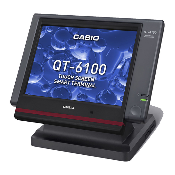
Casio QT-6100 Service Manual
Hide thumbs
Also See for QT-6100:
- Operation manual (18 pages) ,
- User manual (6 pages) ,
- Reference manual (6 pages)

Related Manuals for Casio QT-6100


Summary of Contents for Casio QT-6100
- Page 1 SERVICE MANUAL (without price) ELECTRONIC CASH REGISTER QT-6100 (EX-819) AUG. 2008 QT-6100 INDEX...
-
Page 2: Table Of Contents
CONTENTS QT-6100 PAGE 1. SPECIFICATIONS ..................1 2. INITIALIZATION ....................5 3. DISASSEMBLY .....................9 4. ASSEMBLY ....................15 5. OPTION INSTALLATION ................21 6. IN LINE / ON LINE ..................25 7. DIAGNOSTIC OPERATION ................27 8. CIRCUIT EXPLANATIONS ................47 9. ERROR CODE LIST ..................66 10. IC DATA .......................78 11. -
Page 3: Specifications
<AC input current at Adaptor> In operation Max. 1.1A 1.1A 1.1A 1.1A Display off Max. 0.25A 0.15A 0.15A 0.15A <DC input current at QT-6100> In operation Max. 1.1A 1.1A 1.1A 1.1A Display off Max. 0.5A 0.5A 0.5A 0.5A • Memory protection... - Page 4 1-4. Devices specifications • LCD Display Name NL8060BC31-27 Size 12.1 inch SVGA TFT panel Resolution 800 x 600 Interface CMOS 6 bits Colors 262,144 colors • Touch Panel Name N010-0550-T711 Size 12.1 inch • Panel brightness control 1 x VR controller •...
- Page 5 1-6. Option List CASIO sales options DEVICE NAME MODEL NOTE • Magnet i-Button QT-6011DLS • Display set for customer QT-6060D Connect to Com 3 • Display cable for customer QT-6061CB (for mounting to the base) • Display 5-meter cable for customer QT-6062CB •...
- Page 6 Head of MCR 300,000 times (in a clean office room) ■ Installing Precautions When installing QT-6100, attach the ferrite core to the QT-6100 side. Wind the AC adaptor cable around the ferrite core two times. The ferrite core is packed with QT-6100.
-
Page 7: Initialization
6. After releasing the key, enter “20000” (U.S.), “10000” (other area: English), “40000” (other area: German), “50000” (other area: French), “60000” (other area: Spanish) and press the <OK> key. Init Sw INIT Copyright(C) 2004 CASIO COMPUTER CO.,LTD. All rights reserved. ROM VER. xxxxxx xxxx CREATE... - Page 8 • Case 2: Terminal ID = “2” ~ “32” ——— Select “MAUAL”, if you want to enter IP address manually. IP ADDRESS AUTO (IP address setting line will appear on the screen.) ——— Press <YES> to continue. * The IP address of each terminal should be the unique number from 192.168. 0. 1 to 192.168.255.255.
- Page 9 “2.Init2” and press <YES> key and enter “8888888888” and <YES> key to Init 2. 2-2. SYSTEM INITIALIZATION In this chapter shows how to install QT-6100 systems and peripherals. 2-2-1. How to load IPL (Initial Program Loading) Normally, IPL is not necessary since the terminal has efficient programmable options to meet your circumstances.
- Page 10 2-2-2. IPL Operation If you select “CF card”, insert the CF card into the slot before this step. 1. Select the appropriate method to loading IPL data. xxxxxxx IPL :CF CARD xxxxxxx xxxxxxx xxxxxxx xxxxxxx xxxxxxx IPL :COM1 PORT xxxxxxx xxxxxxx 2.
-
Page 11: Disassembly
3. DISASSEMBLY ■ QT-6100 The photos show a similar model, QT-6000. Therefore the appearance may slightly differ. ▪ The number of COM ports has been changed from 6 to 3. ▪ The speaker has been deleted, and a buzzer has been added on the E819-S1 board. - Page 12 7. Open the CARD SLOT COVER. 8. Remove each screw, and then the PC CARD and the COVER for the CF CARD. CARD SLOT COVER Screws 9. Release the hook and remove the REAR CASE. 10. Remove four screws and the iron plate. 11.
- Page 13 13. Remove the connector for the battery and the battery. 15. Remove four connectors. Connectors × 4 14. Remove twelve screws and the metal bracket. Screw × 3 15. Remove three connectors and one FPC. — 11 —...
- Page 14 16. Remove six screws, one connector, one FPC, three bosses, and then remove the main PCB. Screw × 6 boss Connectors 17. Remove 14 screws and then the LCD unit. Screw × 14 18. Remove two screws, one connector and the inverter PCB. Screw ×...
- Page 15 ■ QT-6060D 1. Remove four screws. 2. Release the connector and remove the IO PCB. Screw × 4 Connector 3. Remove four screws and separate the unit as shown below. Screw × 4 4. Remove the cap. 5. Remove four screws under both packing. Screw ×...
- Page 16 6. Release the hook and remove the REAR CASE. 7. Remove five screws, connector and the HINGE. Screw × 5 8. Remove seven screws and separate the LCD Unit. Screw × 7 — 14 —...
-
Page 17: Assembly
4. ASSEMBLY ■ QT-6100 The photos show a similar model, QT-6000. Therefore the appearance may slightly differ. ▪ The number of COM ports has been changed from 6 to 3. ▪ The speaker has been deleted, and a buzzer has been added on the E819-S1 board. - Page 18 5. Connect one PFC and three connector. Terminal side 6. Fix the iron plate with twelve screws. Screw × 3 7. Connect four connectors. — 16 —...
- Page 19 8. Connect the connector for the battery and assemble the battery. 9. Assemble the IO Unit and fix it with three screws. Connect four connectors and one FPC. Screw × 3 Connectors 10. Fix the iron plate with four screws. Screw ×...
- Page 20 11. Assemble the REAR CASE. Hook the REAR CASE and fix it with ten screws. Screw × 10 12. Fix the PC CARD and the CF CARD COVER. Fix the backup battery cover with one screw. Connect the DRAWER wiring (a cable and an earth). CARD SLOT COVER Screws 13.
- Page 21 ■ QT-6060D 1. Assemble the LCD Unit in the FRONT CASE with seven screws. Screw × 7 2. Connect the connector and fix the HINGE with five screws. Screw × 5 3. After fixing the packing to the REAR CASE, assemble the REAR CASE and the FRONT CASE. Hooks 4.
- Page 22 5. Fix the cap to the LCD Unit. Be careful with the position of the screw holes. 6. Fix the cap to the stand. Be careful with the direction of the cap. The height of the screw hole on the front side should be lower. 7.
-
Page 23: Option Installation
5. OPTION INSTALLATION 5-1. To install the I-Button 1. Remove the REAR COVER for QT-6100 (No.1 to No.10 in the disassembly procedure). 2. Remove one screw and then the I-Button cover. 3. Insert the I-Button. Fix it with a nut. Insert the earth plate. Fix it with a nut. - Page 24 6. Store the core in the main unit, and then fix it with fabric tape. 5-2. To install the MCR 1. Remove the REAR COVER for QT-6100 (No.1 to No.10 in the disassembly procedure). 2. Remove the packing from the main unit.
- Page 25 4. Connect the connector and fix the metal bracket with two screws. NOTE: The lead wires should be stored neatly in a line. 5. Fix the metal bracket to QT-6100 with two screws. 6. Connect the connector to QT-6100. NOTE: Arrange the cables so that they do not tangle with each other.
- Page 26 5-3. REMOTE PRINTER / SLIP PRINTER Connect the following peripherals to the COM ports respectively. REMOTE PRINTER: COM1, 2 or 3 SLIP PRINTER: COM2 PC/MODEM SCANNER DC IN COM1 COM2 COM3 COM1 COM2 COM3 5-4. To install the DRAWER In case of connecting drawer, follow the procedure below. 1.
-
Page 27: Inline / Online
6. IN LINE / OUT LINE With the QT-6100, there are the following inline / online connectors in the rear side of the body. 6-1. Inline interface The maximum inline cable length and the maximum connection unit will be varied by the inline communica- tion speed as shown below figure. - Page 28 8 remote printers in the 3 ~ 32 terminal can be defined. Via COM 1 port of the master terminal or Inline (Ethernet) Maximum 32 terminals QT-6100 (Com1) PC Cable wiring Pin No. Pin No. Signal name Pin No.
-
Page 29: Diagnostic Operation
(2) Turn the power on while pressing the INIT switch. (3) Release the switch when the display shown below appears. * Operation is not guaranteed if the switch is released before the display appears. INIT Copyright(C)2004 CASIO COMPUTER CO.,LTD. All rights reserved. ROM VER xxxxxx xxxx CREATE... - Page 30 7-3. DIAG command input system X X X X X X n Input a command according to the following code. XXXXXX : additional action n : number of times a : action g : group d : device number 7-4. Status Display With the EX820, the following display is displayed on the LCD (SVGA).
-
Page 31: 3 Ram Write/Read Test
7-5. Check item The following test can be checked in the diagnostic test. Device to be checked Operation Note Page Batch test 1 Test Device : RAM, FLASH, Display, Print, Time, Drawer Batch test 2 Test Device : Display, Back light RAM WRITE/READ test n011 RAM READ only test... - Page 32 7-6. Operation of each test [ 1 ] Batch test 1 [Function] RAM test, FLASH test, display test, test print, time setting and drawer open test are performed continuously. Make sure to connect the printer to COM1. [Operation] Refer to the page for the details of the following tests. Operation : The following tests are performed automatically.
- Page 33 [ 3 ] RAM WRITE/READ test [Function] WRITE/READ test for RAM is performed. A counter is displayed for RAM test as follows. [Operation] Operation : n: 01 = One time check (can be omitted) not 0 = Continuous check (To stop the test, press "ESC" key) [LCD] NOTE: Prints the address of the error in case the test ended n011...
- Page 34 [ 5 ] FLASH Check SUM test [Function] This test will check SUM test for FLASH is performed. [Operation] Operation : n: 01 = One time check (can be omitted) not 0 = Continuous check (To stop the test, press "ESC" key) [LCD] FLASH FLASH CHK SUM OK...
- Page 35 [ 7 ] CF-CARD WRITE/READ test [Function] This test will check the write/read test (connection test) for CF-CARD. Perform the CF-CARD clear test, before start of this test. Note that this test does not ensure the data inside the CF-CARD as well as its performance. [Operation] Operation : p : designates PCMCIA SLOT...
- Page 36 [ 9 ] CF-CARD CLEAR test [Function] This test will check the clear test for CF-CARD. Note that this test does not ensure the data inside the CF-CARD as well as its performance. [Operation] Operation : p: designates PCMCIA SLOT 0 = CF 1 = PCMCIA n: 0 = One time check (can be omitted)
- Page 37 [ 11 ] LCD test [Function] This test will check the LCD display. In case of one time check only, the test can be ended by the judgment (OK or NG) of the opera- tor. The display can be switched by the touch of the panel. The display will not change to the next one unless the panel is touched.
- Page 38 [ 12 ] LCD calibration test [Function] This will test the calibration of the LCD (touch panel). * Perform the calibration in the diagnostic mode even when the product is in the market. Make sure to backup the register data when necessary. [Operation] A cross appears at the following four coordinates in the panel one by one.
- Page 39 [ 14 ] Remote Cust DISP test [Function] This test will check whether REMOTE DISP can be displayed. Make sure to connect REMOTE DISP to COM3. In case of one time check only, the test can be ended by the judgment (OK or NG) of the opera- tor.
- Page 40 [ 15 ] External printer print test [Function] This test will check the print test for the RS232C I/F printer. Connect the printer to the COM which is to be tested. [Operation] Operation : x1 x2 x3 X1: Print test pattern (0 = A pattern, 1 = B pattern) X2: Port selection (1 = COM1, 2 = COM2, 3 = COM3) X3: Baud rate selection (1 = 4800 bps, 2 = 9600 bps, 3 = 19.2 kbps) n: 0 = One time check (can be omitted)
- Page 41 [ 16 ] RS232C PORT test [Function] This is the RS232C test. The loop back test for RS232C port is performed by making the connection shown in the figure. Refer to [ 17 ] RS232C PORT batch test the figure for RS232C port connection. [Operation] Operation : x: Baud rate selection...
- Page 42 [ 17 ] RS232C PORT batch test [Function] This is the RS232C port batch test. The loop back test for RS232C port is performed by making the connection shown in the figure. The loop back test is performed from COM1 to COM 3 by the following setting by one time check.
- Page 43 [ 18 ] Ethernet test [Function] This test will check the counter-communication of Ethernet. Always make the receive ECR in the wait mode first and then send data from the send ECR. The counter of the number of successful/failed communication to the LCD is displayed after the communication normally starts.
- Page 44 [ 19 ] MAC (Media Access Control) Address SET [Function] This test will write the MAC address. [Operation] * Once an ID is set, make sure to perform the test using this ID. When changing the ID, turn the power on again. x : Writing the address 1 : Writes the address by manually writing the MAC address In the manual input mode, the test enters the wait mode for the input of MAC address.
- Page 45 [ 20 ] Time setting / [ 21 ] Time display [Function] This sets the time and date. When setting the time, the time and date will be displayed without inputting the fixed value. [Operation] * Date and time setting Operation : x1 x2 x3 x4 x5 x6 a: 0: time setting x1/x2: time, x3/x4: minutes, x5/x6: second 1: time setting x1/x2: year, x3/x4: month, x5/x6: day...
- Page 46 [ 23 ] Buzzer test [Function] This test will check the buzzer function. Ring the one-shot buzzer. [Operation] Operation : n: 0 = One time check (can be omitted) not 0 = Continuous check (To stop the test, press "ESC" key) [LCD] BUZZ n092...
- Page 47 [ 25 ] MCR test [Function] This is a card reader (MCR) test. The test enters the wait mode for only MCR input. The test judges the result between OK and NG by the comparison between already set data and read data. [Operation] Operation : Press [ESC] key to end the test manually.
- Page 48 [ 26 ] Charging test [Function] This test will turn off the charging function. [Operation] Operation : [LCD] CAHRGE OFF [Print] CAHRGE OFF — 46 —...
-
Page 49: Circuit Explanations
8. CIRCUIT EXPLANATION 8-1. BLOCK DIAGRAM — 47 —... - Page 50 8-2. LSI BLOCK DIAGRAM ISDN(MODEM)PORT SERIAL I/F RS232C × 1 (COM1) BUFFER BUFFER CF CARD (IC8, 13, 17) (IC4, 5, 6, 7) SLOT SH BUS RS232C 80Mhz (COM1~3) 10M/100MBASE Ethernet SDRAM PORT 256MB (IC28) (IC35) (IC12) (IC14) (IC19) FROM 128MB (IC1) PCI BUS SVGA...
- Page 51 8-3. RESET CIRCUIT The reset circuit is as follows. 8-4. POWER SUPPLY CIRCUIT 1 VP (DC 19V) For the drawer circuit VOP (DC 5.2V) For the COM2, 3 power and display ON/OFF LED VCC (DC 5V) For the logic circuit power The power supply circuit is as follows.
- Page 52 8-5. POWER SUPPLY CIRCUIT 2 VBAT (DC 3.3V) For the battery V1.5 (DC 1.5V) For the CPU core V1.8 (DC 1.8V) For the PCMCIA core The power supply circuit is as follows. 8-6. DRAWER I/F CIRCUIT The drawer open circuit is as follows. —...
-
Page 53: Pin Assignment
8-7. CPU (IC26: SH7751) 8-7-1. Pin Assignment XTAL2 EXTAL2 VDD-RTC VSS-RTC PCICLK IDSEL /MD9 /MD10 MD6/ MD2/RXD2 QFP256 TCLK MD8/ MD1/TXD2 MD0/SCK2 (Top view) MD7/ AUDSYNC AUDCK AUDATA0 AUDATA1 AUDATA2 AUDATA3 Reserved MD3/ MD4/ VDD (internal) DACK0 VSS (internal) DACK1 DRAK0 DRAK1 VDDQ (IO) -
Page 54: Block Diagram
8-7-2. Block Diagram Lower 32-bit data Cache and I cache ITLB UTLB O cache controller INTC DMAC (SCIF) PCIC (PCI)DMAC BSC: Bus state controller CPG: Clock pulse generator DMAC: Direct memory access controller FPU: Floating-point unit INTC: Interrupt controller ITLB: Instruction TLB (translation lookaside buffer) UTLB: Unified TLB (translation lookaside buffer) External (SH) bus... - Page 55 8-7-3. Pin Function PIN NAME DESCRIPTION Mode (H-UDI) Clock (H-UDI) VDDQ Power IO VDD VSSQ Power IO GND Data in (H-UDI) Chip select 0 Chip select 1 Chip select 4 Chip select 5 Chip select 6 Bus start WE0/REG D7-D0 select signal D15-D8 select signal Data VDDQ...
- Page 56 PIN NAME DESCRIPTION VDDQ Power IO VDD VSSQ Power IO GND Address VDDQ Power IO VDD VSSQ Power IO GND Address CAS2/DQM2 D23-D16 select signal CAS3/DQM3 D31-D24 select signal Data VDDQ Power IO VDD VSSQ Power IO GND Power Internal VDD Power Internal GND Data...
- Page 57 PIN NAME DESCRIPTION WE3/ICIOWR D31-D24 select signal Power Internal VDD Power Internal GND SLEEP Sleep PCIGNT4 Bus grant (host function) PCIGNT3 Bus grant (host function) PCIGNT2 Bus grant (host function) PCIREQ4 Bus request (host function) PCIREQ3/MD10 Bus request (host function)/mode VDDQ Power IO VDD...
- Page 58 PIN NAME DESCRIPTION AD14 AD13 PCI address/data/port AD12 AD11 VDDQ Power IO VDD VSSQ Power IO GND AD10 PCI address/data/port C/BE0 Command/byte enable Power Internal VDD Power Internal GND PCI address/data/port VDDQ Power I/O VDD VSSQ Power I/O GND PCI address/data/port PCI address/data/port IRL0 Interrupt 0...
- Page 59 PIN NAME DESCRIPTION AUDSYNC AUD sync AUDCK AUD clock VDDQ Power IO VDD VSSQ Power IO GND AUDATA0 AUD data AUDATA1 Power Internal VDD Power Internal GND AUDATA2 AUD data AUDATA3 Reserved Do not connect MD3/CE2A Mode/PCMCIA-CE MD4/CE2B Mode/PCMCIA-CE Mode MD5 VDDQ Power IO VDD...
- Page 60 8-8. G/A (IC14: uPD65945GJ-093-JEU) 8-8-1. Pin Function PIN NO PIN NAME I / O D E S C R I P T I N PIN NO PIN NAME I / O D E S C R I P T I N VDD VDD VDD VDD ARC DATA (D0)
- Page 61 8-9. SDRAM (IC12: HY5V52ALFP-H-C) 90-ball FBGA DQ26 DQ24 DQ23 DQ21 DQ28 VDDQ VSSQ VDDQ VSSQ DQ19 VSSQ DQ27 DQ25 DQ22 DQ20 VDDQ VSSQ DQ29 DQ30 DQ17 DQ18 VDDQ VDDQ DQ31 DQ16 VSSQ DQM3 DQM2 /RAS DQM1 NC /CAS /WE DQM0 VDDQ DQ8 DQ7 VSSQ VSSQ DQ10 DQ9...
- Page 62 8-10. DISPLAY CONTROLLER (IC45: SM712) 8-10-1. Pin Assignment MD12 MD31 MD17 MD28 MD20 MD25 MD22 AD12 AD14 ~BE2 ~FRAME MD11 ~DQM3 MD30 MD18 MD27 MD21 MD24 ~BE0 AD10 AD13 ~BE1 ~TRDY ~STOP AD16 MD29 MD15 MD13 MD10 ~DQM2 MD16 MD19 MD26 MD23 AD11...
- Page 63 8-10-2. Pin Function PIN NAME DESCRIPTION Host Interface AD [31:0] PCI multiplexed Address and Data Bus. A bus transaction consists of an address cycle followed by one or more data cycles. PCI Bus Command and Byte Enables. These signals carry the bus command during the address cycle and ~BE [3:0] byte enable during data cycles.
- Page 64 PIN NAME DESCRIPTION External Display Memory Interface MA [9:0] External Memory Address Bus. The video memory row and column addresses are multiplexed on these lines. MD [63:0] External Memory Data Bus External Memory Write Strobe ~RAS External Memory SDRAM Row Address Select ~CAS External SGRAM Column Address Select ~CS0...
- Page 65 PIN NAME DESCRIPTION CRT Interface Analog Red Current Output GREEN Analog Green Current Output BLUE Analog Blue Current Output IREF Current Reference Input CRTVSYN- CRT Vertical Sync CRT Horizontal Sync or Composite Sync depending on CCR65 [0] CRTH- 0 = CRT Horizontal Sync 1 = Composite Sync Video Port Interface P [15:0]...
- Page 66 PIN NAME DESCRIPTION VCC and GROUND Pins HVDD Host Interface VDD on I/O Ring, 3.3V MVDD Display Memory Interface VDD on I/O Ring, 3.3V FPVDD Flat Panel Interface VDD on I/O Ring, 3.3V VPVDD VPVDD VPort Interface VDD on I/O Ring 3.3V CVDD Clock (PLL) Analog Power, 3.3V AVDD...
- Page 67 8-11. ETHERNET CONTROLLER (IC28: LAN91C113) 8-11-1. Pin Assignment 8-11-2. Block Diagram — 65 —...
-
Page 68: Error Messages
9. ERROR CODE LIST Error messages When an error occurs on a QT-6100 terminal, a buzzer sounds and the appropriate error message appears on the main display, indicating what action to take. The following table lists the error messages and describes the action to take. - Page 69 Meaning Action Prompt message E051 CHK/TBL No. is occu- Attempt is made to use the <NEW Finalize and close the check that is currently pied. CHECK> key to open a new check us- under the number that you want to use or ing a number that is already used for an use a different check number.
- Page 70 Meaning Action Prompt message ********** Time out at ECR which has printer Follow the prompt message. E073 Your receipt/order may “****” means ECR logical ID and printer not be issued. number. YES:Retry to print. NO :Backup to R/J printer. ESC:Discard data. E075 Negative Balance, can- Attempted finalization when balance is Register item(s) until the balance becomes...
- Page 71 Meaning Action Prompt message E140 Wrong menu. This sheet holder is prohibited by pro- Set correct sheet holder. gram. E141 Press <TRAY TTL> <TRAY TOTAL> key is not pressed twice Follow the prompt message. twice before finalization. before finalization. E145 Arrangement syntax er- Arrangement syntax error Program the arrangement again.
- Page 72 Meaning Action Prompt message E200 Insert CF Card. CF card is not inserted to the slot. Insert CF card. E201 Format error. CF card data or formats illegal. Check the CF card. E203 Insufficient memory. Insufficient memory is remained in CF Format or use a new CF card.
- Page 73 Operation prompt All prompt messages, together with descriptors and symbol characters for displaying / printing are contained in the list below. These messages cannot be added, modified or deleted. Meaning Prompt message Data cannot be printed out. Request to check the X / Z report data which cannot Backup to R/J printer? be printedout.
- Page 74 System error code All error codes are contained in the list below. These error codes are displayed or printed on error log report. Error code Meaning 0010 Handler access error (software) 0011 Cannot execute handler (system configuration) 0012 Break by PC 0013 Break by ECR 0014...
- Page 75 Error code Meaning 0079 Z lock release error on satellite terminal 0081 Check tracking master is removed from system. 0082 Check tracking backup master is removed from system. 0128 Parameter error / Maximum length of send error 0130 Error drive 0134 Network parameter error 0138...
- Page 76 9-4. OS Fatal Error When a fatal error occurs during an operation of the operating system, normal operation becomes im- possible afterwards. Therefore, the OS displays a message as shown below and stops the operation of ECR. Such errors include errors of the OS (ITRON) itself, driver system errors, etc. The values of Error No.
- Page 77 Description of Errors (1) Semaphore acquisition error Error No. -1 / -4 / -6 Description of phenomenon: This is a system error in ITRON. This phenomenon may occur when the exclusion function of ITRON is used. Possible causes: A software bug or an illegal operation of ITRON. (2) Mailbox creation error Error No.
- Page 78 error point: Indicates the point on the memory where the operation instruction that causes the above general exception is located (program counter). However, an illegal address may be displayed depending on the exception code. access adrs: Indicates the address that is accessed according to the operation instruction that causes the above general exception.
- Page 79 (8) error no. 180: Reservation instruction code exception (9) error no. 1A0: Slot illegal instruction exception Description of phenomenon: These exceptions occur when an illegal instruction is performed. Possible causes: It is hard to think that this phenomenon is caused by software, because these errors occur due to an internal operation of the CPU.
- Page 80 10. IC DATA ■ MAIN PCB (E820-1 PCB) 1. ALVCH16244 (IC13, 17) logic diagram (positive logic) terminal assignments FUNCTION TABLE (each 4-bit buffer) INPUTS OUTPUT OUTPUT V CC V CC V CC V CC No internal connection — 78 —...
- Page 81 2. ALVCH16245 (IC8) logic diagram (positive logic) 1DIR 1DIR To Seven Other Channels 2DIR terminal assignments FUNCTION TABLE (each 8-bit section) INPUTS 1DIR OPERATION OPERATION B data to A bus V CC V CC A data to B bus Isolation V CC V CC 2DIR...
- Page 82 3. BR93L46RF (IC35) Pin Name Function Power Supply INPUT Chip Selct INPUT Serial Clock Input Start bit,Cord,Address,Serial data OUTPUT Serial data input, READY/BUSY status 4. HD74LV00 (IC29) 5. HD74LV74 (IC25) FUNCTION TABLE INPUTS OUTPUTS 1CLR 2CLR 1CLK 1PRE 2CLK 2PRE * This configuration is nonstable;...
- Page 83 6. HD74LVC08 (IC20) 7. HD74LVC138 (IC11) 14 V GND 8 8. HD74LVC244 (IC4,5) Inputs Output Y H : High L : Low Don’t care High impedance 9. HD74LVC245 (IC6,7) Inputs Output Y T / R Bus B Data to Bus Bus A Data to Bus B H : High L : Low...
- Page 84 10. HIN202CBNZ-T (IC24) 0.1 F +5V TO 10V 0.1 F VOLTAG E INVERTER +10V TO -10V 0.1 F VOLTAG E INVERTER 0.1 F 400k OU T 400k OU T 11. HIN211CAZ-T (IC3,9,23,27) 0.1 F 0.1 F +5V TO 10V VOLTA GE DOUBLER +10V TO -10V 0.1 F VOLTAGE INVERTER...
- Page 85 12. IDT2305 (IC40) FUNCTIONALBLOCKDIAGRAM CLKOUT CLKOUT CLK2 CLK4 CLK1 CLK1 Control Logic CLK2 CLK3 CLK4 13. M51957BFP (IC33) POWER POWER INPUT 25uA OUTPUT INPUT OUTPUT DELAY VALUE 1.25V DELAY VALUE 14. RTC-7301DG (IC19) Control Line 32.768 kHz Digital Trimming FOUT DIVIDER REGISTER Temperature...
- Page 86 15. S-80828CLNB-B6N-T2 (IC55) RF.F 16. SG-8002JFSCB14.318M (IC41): Programmable High-Frequency Crystal Oscillator (14.318 MHz) SG-8002JFSCB33M (IC43): Programmable High-Frequency Crystal Oscillator (33 MHz) 17. SN74AHCT08 (IC49) 14 V — 84 —...
- Page 87 18. SN74HC148 (IC32) logic diagram (positive logic) FUNCTION TABLE INPUTS OUTPUTS 19. SN74LV04APWR (IC10) 20. SSN74LV07A (IC37) — 85 —...
- Page 88 21. SN74LV08APWR (IC47,57) 22. SN74LV10APWR (IC30) 14 V 14 V 23. SN74LV244APWR (IC22,38,39) Inputs Output Y H : High L : Low Don’t care High impedance 24. SN74LV32APWR (IC48,52~54) 14 V — 86 —...
- Page 89 25. SN74LV374APWR (IC16,21,50,51) FUNCTION TABLE INPUTS OUTPUT 26. SN74LVC1G08 (IC56) 14 V 27. SN74LVC1G97 (IC58,59) FUNCTION TABLE INPUTS OUTPUT logic diagram (positive logic) — 87 —...
- Page 90 28. XC6206P182MR (IC34) PIN ASSIGNMENT PIN NUMBER FUNCTION NAME Ground VOUT Output VOUT Power Input BLOCK DIAGRAM Current Limit Voltage Reference 29. XC6219B332MR (IC46) (NC) PIN ASSIGNMENT PIN NUMBER FUNCTION NAME Input Ground ON/OFF Control No Connection VOUT Output BLOCK DIAGRAM ON/OFF each circuit Control...
- Page 91 30. XC62EP1502MR (IC42) CE/CE PIN ASSIGNMENT PIN NUMBER FUNCTION NAME Ground Supply voltage input VOUT VOUT Regulated voltage output Base current control CE/CE Chip enable 31. XC6365A363MR (IC2) (FB) Phase Compensation Error Amp Controler Buffer, EXT / Drive EXT/ Vref whth Ramp Wave PWM/PFM Soft Start,...
-
Page 92: Pcb Layout
11. PCB LAYOUT MAIN PCB (E819-1 PCB) (TOP VIEW) — 90 —... - Page 93 MAIN PCB (E819-1 PCB) (BOTTOM VIEW) — 91 —...
- Page 94 E819-S1 INTERFACE PCB ( PCB) (TOP VIEW) (BOTTOM VIEW) LED PCB (E820-LED PCB) (TOP VIEW) (BOTTOM VIEW) — 92 —...
-
Page 95: Circuit Diagrams
12. CIRCUIT DIAGRAM MODEL : QT-6100 (EX-819) CONTENTS 1. MAIN PCB CIRCUIT 2-1.MAIN PCB CIRCUIT (1/11) ..................94 2-2.MAIN PCB CIRCUIT (2/11) ..................95 2-3.MAIN PCB CIRCUIT (3/11) ..................96 2-4.MAIN PCB CIRCUIT (4/11) ..................97 2-5.MAIN PCB CIRCUIT (5/11) ..................98 2-6.MAIN PCB CIRCUIT (6/11) ..................99 2-7.MAIN PCB CIRCUIT (7/11) ..................100... - Page 96 Model Board No. Name Drawing No. QT-6100 E819-1 MAIN BOARD (1/11) CASIO COMPUTER CO.,LTD. (EX-819) — 94 —...
- Page 97 Model Board No. Name Drawing No. QT-6100 E819-1 MAIN BOARD (2/11) CASIO COMPUTER CO.,LTD. (EX-819) — 95 —...
- Page 98 Model Board No. Name Drawing No. QT-6100 E819-1 MAIN BOARD (3/11) CASIO COMPUTER CO.,LTD. (EX-819) — 96 —...
- Page 99 Model Board No. Name Drawing No. QT-6100 E819-1 MAIN BOARD (4/11) CASIO COMPUTER CO.,LTD. (EX-819) — 97 —...
- Page 100 Model Board No. Name Drawing No. QT-6100 E819-1 MAIN BOARD (5/11) CASIO COMPUTER CO.,LTD. (EX-819) — 98 —...
- Page 101 Model Board No. Name Drawing No. QT-6100 E819-1 MAIN BOARD (6/11) CASIO COMPUTER CO.,LTD. (EX-819) — 99 —...
- Page 102 Model Board No. Name Drawing No. QT-6100 E819-1 MAIN BOARD (7/11) CASIO COMPUTER CO.,LTD. (EX-819) — 100 —...
- Page 103 Model Board No. Name Drawing No. QT-6100 E819-1 MAIN BOARD (8/11) CASIO COMPUTER CO.,LTD. (EX-819) — 101 —...
- Page 104 Model Board No. Name Drawing No. QT-6100 E819-1 MAIN BOARD (9/11) CASIO COMPUTER CO.,LTD. (EX-819) — 102 —...
- Page 105 Model Board No. Name Drawing No. QT-6100 E819-1 MAIN BOARD (10/11) CASIO COMPUTER CO.,LTD. (EX-819) — 103 —...
- Page 106 Model Board No. Name Drawing No. QT-6100 E819-1 MAIN BOARD (11/11) CASIO COMPUTER CO.,LTD. (EX-819) — 104 —...
- Page 107 Model Board No. Name Drawing No. QT-6100 E819-S1 INTERFACE PCB CASIO COMPUTER CO.,LTD. (EX-819) — 105 —...
- Page 108 Model Board No. Name Drawing No. QT-6100 E820-LED CASIO COMPUTER CO.,LTD. (EX-819) — 106 —...
- Page 109 Model Board No. Name Drawing No. QT-6060 EDP-1 MAIN BOARD (1/2) CASIO COMPUTER CO.,LTD. (EX-DP-UNIT-16) — 107 —...
- Page 110 Model Board No. Name Drawing No. QT-6060 EDP-1 MAIN BOARD (2/2) CASIO COMPUTER CO.,LTD. (EX-DP-UNIT-16) — 108 —...
- Page 111 Model Board No. Name Drawing No. QT-6100 EDP-CNB1 SUB BOARD CASIO COMPUTER CO.,LTD. (EX-DP-UNIT-16) — 109 —...
-
Page 112: Parts List
2. As for spare parts order and supply, refer to the “GUIDEBOOK for Spare Parts Supply”, published separately. 3. The numbers in item column corespond to the same numbers in drawing. 4. CASIO does not supply the spare parts without parts code. 5. Remarks Q'ty :... - Page 113 EXPLODED VIEW (QT-6100) — 111 —...
- Page 114 1 Standard Model USA 2 Standard Model Other 3 Dallas key Model Q'ty Price Item Code No. Parts Name Specification Rank Code 1. MAIN PCB BLOCK 10315646 PCB ASSY/E819-1 RJE502692*001V01 IC45 SM712GX04LF02-BA IC40 IDT2305A-1DCG IC28 LAN91C113-NU IC26 10164750 HD6417751RF240 IC14 10205905 UPD65945GJP16-JEUA IC44...
- Page 115 1 Standard Model USA 2 Standard Model Other 3 Dallas key Model Q'ty Price Item Code No. Parts Name Specification Rank Code R7,12-18,23-27, 29,30,34,35,37,41, 43-48,54,62,64, 96,103,108,113, 135-174,183-192, 199,200,203-212, RESISTOR/CHIP WR06X103JTL 224-234,237-239, 241,244,245,251, 253,254,257-260, 263,269-271,296, 298-308,311-313, 315-318,331,335 R252,276,278, RESISTOR/CHIP WR06X104JTL 279,319,320 R33,333 RESISTOR/CHIP WR06X105JTL...
- Page 116 1 Standard Model USA 2 Standard Model Other 3 Dallas key Model Q'ty Price Item Code No. Parts Name Specification Rank Code RM22,24-27,29-36, 39,40,42-45,49, REGISTOR ARRAY WA06X330JTL 60,62-65,71-74, 81,84,87,89 RM68-70,76,91,93 REGISTOR ARRAY WA06X510JTL RM2,95,97-106 REGISTOR ARRAY WA06X563JTL C199 CAPACITOR/CHIP CERA 0603B103K500CT C4,6-12,15-18, 23-25,30-35,37,...
- Page 117 1 Standard Model USA 2 Standard Model Other 3 Dallas key Model Q'ty Price Item Code No. Parts Name Specification Rank Code Q9,13 TRANSISTOR/CHIP DIGITAL DTC114TETL Q3,6,8,11,15 22592674 TRANSISTOR/CHIP DIGITAL DTC114YETL TRANSISTOR/CHIP 2SA1729S-TD-E TRANSISTOR/CHIP 2SA2012-TD-E TRANSISTOR/CHIP 2SA2018-TL TRANSISTOR/CHIP 2SJ499-TL-E TRANSISTOR/CHIP RTF020P02TL 10166828 INDUCTOR/CHIP POER...
- Page 118 1 Standard Model USA 2 Standard Model Other 3 Dallas key Model Q'ty Price Item Code No. Parts Name Specification Rank Code N 16 10165823 COVER/DP SW E820 RJE501090-001V01 N 17 10165824 SEAL/MCR E820 RJE501106-001V01 N 18 10165825 CHASSIS/LR E820 RJE501108-001V01 N 19 10165826...
- Page 119 1 Standard Model USA 2 Standard Model Other 3 Dallas key Model Q'ty Price Item Code No. Parts Name Specification Rank Code D4,5 DIODE/CHIP 1SR154-400TE25 10183841 CONNECTOR IMSA-9610S-25FY914 10204413 CONNECTOR B4P-VH(LF)(SN) CN6,7 CONNECTOR S3BPHSM4TB(LF)(SN) CN3,4,5 30007917 CONNECTOR ID9P33E4GX28 CONNECTOR B2B-XH-A(LF)(SN) CONNECTOR CJ214 10241792...
- Page 120 EXPLODED VIEW (QT-6060D) Sales Option — 118 —...
- Page 121 Price Item Code No. Parts Name Specification Q'ty Rank Code 1. DISPLAY PCB BLOCK 1016 6273 PCB ASSY/EDP-1 RJE501147*001V01 N IC6 D784216AGC8EUDB01 N IC9 1016 6277 LSI LE28F4001CTS-12L01 1016 6792 IC HIN211CAZ-T 1009 7860 IC/MOS XC6201P332MR 1015 6876 IC LM2611BMF 1012 0131 IC/CMOS SN74LVC08APWR N IC4...
- Page 122 Price Item Code No. Parts Name Specification Q'ty Rank Code 2. DISPLAY BLOCK 1016 6707 CASE/FRONT EDP RJE501139-001V01 1012 6583 CUSION/LCD V E466 RJE500659-001V01 1012 6584 CUSION/LCD H E466 RJE500659-002V01 1012 0084 LCD UNIT MDG12DC38-FC 1016 8763 CHASSIS/DP EDP RJE501122-001V01 1016 8764 CABLE SUB ASSY/CNB1 RJE501195*001V01 HINGE ASSY...
- Page 123 12. DRAWER (DL-2425) — 121 —...
- Page 124 DL-2425(M type) Price N Item Code No. Parts Name Specification Qt'y Rank code CASE/MAIN RJE500529-001 NOT SUPPLY 1012 0508 PLATE/BOTTOM RJE500534-001 1012 0509 CHASSIS/LEFT RJE500532-001 1012 0510 CHASSIS/RIGHT RJE500533-001 1012 0511 COVER/TOP E240850-4 1012 0523 CHASSIS/BOTTOM RJE500531-001 1012 0528 LOCK SUB ASSY RJE500538*001 6246 5010 SPRING/PRESS E412069-1...
- Page 125 13. DRAWER (DL-2525) — 123 —...
- Page 126 DL-2525(M type) Price N Item Code No. Parts Name Specification Qt'y Rank code CASE/MAIN RJE500529-001 NOT SUPPLY 1012 0508 PLATE/BOTTOM RJE500534-001 1012 0509 CHASSIS/LEFT RJE500532-001 1012 0510 CHASSIS/RIGHT RJE500533-001 1012 0511 COVER/TOP E240850-4 1012 0523 CHASSIS/BOTTOM RJE500531-001 1012 0528 LOCK SUB ASSY RJE500538*001 6246 5010 SPRING/PRESS E412069-1...
- Page 127 14. DRAWER (DL-2785) — 125 —...
- Page 128 DL-2785(M type) Price N Item Code No. Parts Name Specification Qt'y Rank code CASE/MAIN RJE500529-001 NOT SUPPLY 1012 0508 PLATE/BOTTOM RJE500534-001 1012 0509 CHASSIS/LEFT RJE500532-001 1012 0510 CHASSIS/RIGHT RJE500533-001 1012 0511 COVER/TOP E240850-4 1012 0523 CHASSIS/BOTTOM RJE500531-001 1012 0528 LOCK SUB ASSY RJE500538*001 6246 5010 SPRING/PRESS E412069-1...
- Page 129 15. DRAWER (DL-2786) — 127 —...
- Page 130 DL-2786(M type) Price N Item Code No. Parts Name Specification Qt'y Rank code CASE/MAIN RJE500529-001 NOT SUPPLY 1012 0508 PLATE/BOTTOM RJE500534-001 1012 0509 CHASSIS/LEFT RJE500532-001 1012 0510 CHASSIS/RIGHT RJE500533-001 1012 0511 COVER/TOP E240850-4 1012 0523 CHASSIS/BOTTOM RJE500531-001 1012 0528 LOCK SUB ASSY RJE500538*001 6246 5010 SPRING/PRESS E412069-1...
- Page 131 16. DRAWER (DL-2920) — 129 —...
- Page 132 DL-2920(M type) Price N Item Code No. Parts Name Specification Qt'y Rank code CASE/MAIN RJE500529-001 NOT SUPPLY 1012 0508 PLATE/BOTTOM RJE500534-001 1012 0509 CHASSIS/LEFT RJE500532-001 1012 0510 CHASSIS/RIGHT RJE500533-001 1012 0511 COVER/TOP E240850-4 1012 0523 CHASSIS/BOTTOM RJE500531-001 1012 0528 LOCK SUB ASSY RJE500538*001 6246 5010 SPRING/PRESS E412069-1...
- Page 133 17. DRAWER (DL-2921) — 131 —...
- Page 134 DL-2921(M type) Price N Item Code No. Parts Name Specification Qt'y Rank code CASE/MAIN RJE500529-001 NOT SUPPLY 1012 0508 PLATE/BOTTOM RJE500534-001 1012 0509 CHASSIS/LEFT RJE500532-001 1012 0510 CHASSIS/RIGHT RJE500533-001 1012 0511 COVER/TOP E240850-4 1012 0523 CHASSIS/BOTTOM RJE500531-001 1012 0528 LOCK SUB ASSY RJE500538*001 6246 5010 SPRING/PRESS E412069-1...
- Page 135 18. DRAWER (DL-3616) — 133 —...
- Page 136 DL-3616 (L type) Price N Item Code No. Parts Name Specification Qt'y Rank code 1907 7272 LOCK ASSY ZD00290-0 1906 0672 M4XP0.7 9487 0383 LABEL DL-3616 1907 9613 WIRE/FG ZD31670 1907 0223 CONNECTOR 1625-03PI 1902 7112 GROMET 1902 7076 SPRING ZD01370B 1902 6829 RUBBER/DAMPER...
- Page 137 19. DRAWER (DL-3617) — 135 —...
- Page 138 DL-3617 (L type) Price N Item Code No. Parts Name Specification Qt'y Rank code 1907 7935 LOCK ASSY ZD00280-0 1906 0672 M4XP0.7 9487 0384 LABEL DL-3617 1907 9613 WIRE/FG ZD31670 1907 0223 CONNECTOR 1625-03PI 1902 7112 GROMET 1902 7076 SPRING ZD01370B 1902 6829 RUBBER/DAMPER...
- Page 139 CASIO COMPUTER CO.,LTD. Overseas Service Division 6-2, Hon-machi 1-Chome Shibuya-ku, Tokyo 151-8543, Japan...