NAD C521 Service Manual
Cd player
Hide thumbs
Also See for C521:
- Owner's manual (44 pages) ,
- Owner's manual (8 pages) ,
- Service manual (22 pages)
Table of Contents
Advertisement
Advertisement
Table of Contents

Related Manuals for NAD C521


Summary of Contents for NAD C521
- Page 1 C 521 COMPACT DISC PLAYER...
-
Page 2: Safety Information
SAFETY INFORMATION CAUTION CAUTION VARING - INVISIBLE LASER RADIATION WHEN OPEN AND - OSYNLING LASERSTRÅLNING NÄR DENNADEL ÄR INTERLOCKS DEFEATED. AVOID EXPOSURE TO BEAM. ÖPPNAD OCH SPÄRRAR ÄR URKOPPLADE. STRÅLEN ÄR FARLIG. CLASS 1 VARO! - AVATTAESSAJASUOJALUKITUS OHITETTAESSAOLET ADVARSEL - USYNLIG LASERSTRÅLING NÅR DEKSEL ÅPNES OG ALTTIINANÄKTMÄTÖNTÄ... -
Page 3: Table Of Contents
SERVICE SAFETY PRECAUTIONS Replacing the fuses CAUTION: FOR CONTINUED PROTECTION AGAINST THE RISK OF FIRE REPLACE ONLY WITH SAME TYPE OF FUSE. Reference No Part Number Description M502-M504 5120-0020-0 FU T1A 250V UL/CSA 5X20MM M502-M504 5120-0018-0 FU T1A 250V SEMKO/UDE 5X20MM M505 5120-0052-0 FUSE T1.6A 250V 5X20MM UL/CSA... -
Page 4: Specifications
SPECIFICATIONS Disc Capacity ......One Disc, 120 or 80 mm Decoding ....... . BURR-BROWN Delta Sigma 20bit Digital Filter . -
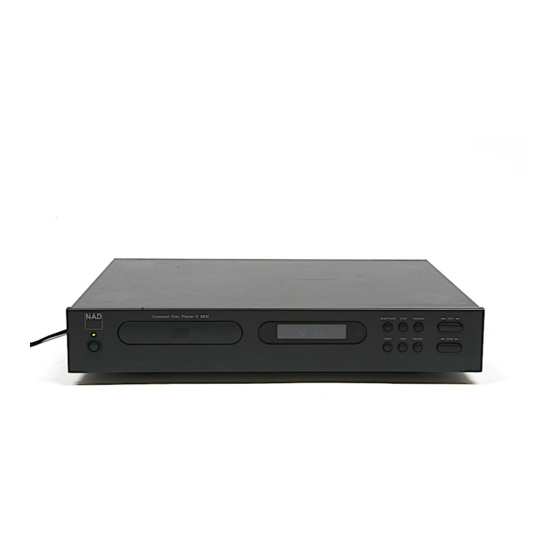
Page 5: Rear Panel / Front Panel
REAR PANEL / FRONT PANEL REAR PANEL 1. LINE OUT 3. AC LINE CORD 2. DIGITAL OUT FRONT PANEL 1. POWER ON / OFF 7. STOP 2. DISC DRAWER 8. REPEAT 3. DISPLAY 9. RANDOM 4. OPEN 10. SCAN Back ( ) / Forward ( 5. -
Page 6: Disassembly Instructions
DISASSEMBLY INSTRUCTIONS 1. Remove machine screws M 4.0 x 6.0 ( 1 to 4 ) from the side panels. Remove tapping screw 3.0 x 8.5 5 from the back panel. Refer to Figure No.1. Figure No.1 2. Pull both sides of the TOP COVER slightly outwards 6 and tilt approx. 35˚ and then remove in the direction as indicated by the arrow 7 . -
Page 7: Block Diagram
BLOCK DIAGRAM... -
Page 8: Wiring Diagram
WIRING DIAGRAM... -
Page 9: Rf Pattern Testing
RF PATTERN TESTING Testing Point NAD - C 521 PCB TESTING POINTS DIAGRAM TESTING PROCEDURE (1) Load the test disc (Sony Test CD YEDS-7) and set the unit into PLAY mode. (2) Connect the scope to R132 (Pin 41 of U101) and DGND (J334). -
Page 10: Important Notes
IMPORTANT NOTES INSTRUCTION FOR HANDLING OPTICAL SYSTEM BLOCK PICK-UP Electrostatic breakdown of the laser diode in the optical system block may occur due to a poten- tial difference caused by electrostatic charge accumulated on clothing, human body, etc. A ground must be provided as follows to prevent any electrostatic charge during unpacking or repair work. - Page 11 PRECAUTIONS WHEN CHANGING LASER PICK-UP When removing the pick-up assembly, short circuit the PCB tracks on the optical block as show in the drawing in order to protect the pick-up before removal. NOTE: Replacement pick-up assemblies are supplied with the PCB pattern already protected. DO NOT REMOVE THE SHORT CIRCUITS UNTIL YOU HAVE FINISHED FITTING THE PICK- Protective soldering place for laser diode...
-
Page 12: Pcb Layout
PCB LAYOUT TRANSFORMER BOARD L401 J401 J407 J402 J406 LIVE BOARD KEY BOARD DISPLAY BOARD... - Page 13 MAIN BOARD...
-
Page 14: Schematic Diagram
SCHEMATIC DIAGRAM 0V *1.8V *1.4V 4.6V 1.7V 1.5V *0.3V 0V 2.3V 2.5V 2.4V 2.5V 1.6V *0.4V 0V 4.8V *0V 4.9V 4.8V *1.2V 0.2V 2.4V 4.9V *1.2V 3V 2.4V 4.9V 2.1V 4.9V 2.3V 2.3V 2.3V 3V *1.6V 2.3V 2.4V 2.4V 2.4V 4.9V 2.4V 2.5V... -
Page 15: Ic Block Diagram
IC BLOCK DIAGRAM U101: LA9240 57 56 55 54 53 52 51 50 48 NC RF DET FIN2 47 TBC FIN1 46 FSC µ - com 45 DGND INTER FACE 44 SLI 43 SLC 42 RFS– TE– 41 RFSM RF Amp TESI T.SERVO &... - Page 16 U302: PCM1710U LRCIN ML/DSD Input Interface MC/DM2 Digital Mode Filter Control BCKIN MC/DM1 CLKO MUTE Timing Control MODE CKSL Noise Shaper DGND DGND 5-Level DAC 5-Level DAC Right Left VCC2R VCC2L AGND2R AGND2L Low Pass Filter Low Pass Filter Right Left EXT1R EXT1L...
- Page 17 U701: LB1641 OUT1 VCC2 OUT2 VCC1 Input logic circuit U201: LA6541D...
- Page 18 U401: LC587206A 48 47 46 45 44 43 42 41 40 39 38 37 36 35 34 33 SEG14 SEG15 SEG16 SEG17 SEG18 SEG19 SEG20 SEG21 SEG22 SEG23 COM4 COM3 COM2 COM1 CUP1 CFOUT CUP2 CFIN 9 10 11 12 13 14 15 16 S port K port M port...
-
Page 19: Troubleshooting Guide
TROUBLESHOOTING GUIDE SET POWER SWITCH TO ON. CHECK FUSES M502, M503, CHECK POWER SUPPLY POWER SUPPLY PATTERNS OPEN IS POWER TURNED ON ? M504, M505 OPEN ? CIRCUIT NORMAL ? OR U501-U504,U506-U507 DEFECTIVE. IS OSCILLATOR CIRCUIT M502, M503, M504, M505 CRYSTAL M401 DEFECTIVE. -
Page 20: Electrical Parts List
ELECTRICAL PARTS LIST Reference No. Part No. Description DISPLAY ASSEMBLY PCB BOARD 1000 PCB-N0980C-DISP DISPLAY ASSEMBLY M501 2460-1340-1 LCD DISPLAY BACKLIGHT M502 2450-1146-0 EL BACKLIGHT IR SENSOR M113 4816-043T-3 IR SENSOR PIC-26043TM2 KODENSHI KEYBOARD ASSEMBLY PC BOARD 2000 PCB-N0980C-KEY KEYBOARD ASSEMBLY SWITCHES M101-M104, M106 5200-3538-0... - Page 21 Reference No. Part No. Description CAPACITORS C101 150F-104K-5-II CC 50V 0.1µF 10% RL 5X5 C104 153F-333J-5-MS CM 50V 0.033µF 5% RL 7X10 C105 150F-331K-5-GE CC 50V 330pF 10% RL 4X3 C106 153F-473J-5-NR CM 50V 0.047µF 5% RL 7.5x9.5 C107 157F-104M-5-IU CE 50V 0.1µF 20% RL 5x11 C108 150F-332K-5-OF...
- Page 22 CE 10V 220µF 20% RL 6x12 C512, C513 157D-108M-5-S9 CE 16V 1000µF 20% RL 10X20 C518 157E-107M-5-KW CE 25V 100µF 20% RL 6x12 C521 150F-104K-5-II CC 50V 0.1µF 10% RL 5X5 C522 157D-107M-5-IU CE 16V 100µF 20% RL 5x11 C523 157F-225M-5-IU CE 50V 2.2µF 20% RL 5x11...
- Page 23 Reference No. Part No. Description TRANSFORMER M501 1806-2320-0 TRANSFORMER STEP-UP 5V TO 83.5V TRANSISTORS Q101 4851-015Y-5 TR 2SA1015-Y HFE120-240 Q301-Q304 4860-1780-5 TR 2SD655F HFE:600-1200 Q305 485A-1346-5 TR 2SA1346 HFE 50-100 Q401 4860-0660-5 TR 2SA1015 (G.R.) RL Q402 4851-012F-5 TR 2SD1012F/G HFE 160~560 Q403 4860-0660-5 TR 2SA1015 (G.R.) RL...
- Page 24 Reference No. Part No. Description R379, R380 4701-151J-C RCF 1/8W 150R 5% ATS R381, R382 4701-472J-C RCF 1/8W 4.7K 5% ATS R383 4701-151J-C RCF 1/8W 150R 5% ATS R384 4701-750J-C RCF 1/8W 75R 5% ATS R390-R393 4717-221J-C RMF 1/2W 220R 5% ATS R401, R402 4701-104J-C RCF 1/8W 100K 5% ATS...
-
Page 25: Mechanism Exploded View
MECHANISM EXPLODED VIEW CD11CA... -
Page 26: Mechanism Exploded View Parts List
MECHANISM EXPLODED VIEW PARTS LIST ITEM Part No. Description 4102-6101-0 RUBBER CUSHION (HARD) 4102-6102-0 RUBBER CUSHION (SOFT) 4102-6103-0 BASE 4102-6104-0 TRAY 4102-6105-0 CDM MOUNTING BASE 4102-6106-0 MAGNET HOLDER 4102-6107-0 SLIDE GEAR 4102-6108-0 PULLEY GEAR 4102-6109-0 DRIVE GEAR 4102-6110-0 PULLEY MOTOR 4102-6111-0 SQUARE BELT 4102-6112-0... -
Page 27: Exploded View Of Laser Cd11A-G
EXPLODED VIEW OF LASER CD11CA-G... - Page 28 EXPLODED VIEW PARTS LIST OF LASER CD11CA-G ITEM Part No. Description 4102-6214-0 ASSY PICKUP LASER P101N 4102-6215-0 ASSY MOTOR 6.0V SPINDLE 4102-6216-0 ASSY MOTOR SLED 6.0V 4102-6217-0 CHASSIS 4102-6218-0 COVER GEAR 4102-6219-0 SHAFT SLIDE 4102-6220-0 GEAR MIDDLE 4102-6221-0 GEAR DRIVE 4102-6222-0 SWITCH LEAF(PWB MOTOR) 4102-6223-0...
-
Page 29: Exploded View
EXPLODED VIEW... -
Page 30: Exploded View Parts List
EXPLODED VIEW PARTS LIST ITEM Part No. Description 0001 1465-5703-2 FASCIA W/SS PAINT 0002 1402-3781-2 STRAP 0003*AH 1402-3516-0 CHASSIS W/SS PAINT 0003*C 1402-3517-0 CHASSIS W/SS PAINT 0005 1402-3530-0 COVER 0006 2442-1000-0 POWER BUTTON 0007 1464-6011-3 CD DOOR W/SS PAINT 0008 3716-4313-0 WINDOW LENS W/SS 0010... -
Page 31: Packing Diagram
REMOTE CONTROL HANDSET 1497-1302-1 REMOTE CONTROL POLYBAG 4301-4104-1 INSTRUCTION MANUAL 1497-1062-0 MANUAL POLYBAG 1435-4300-1-2 CARTON BOX Proprietary information for servicing purposes only. The information herein may not be used com- mercially without the prior written agreement of NAD Electronics International, Toronto, Canada. - Page 32 © NAD 2001 NAD ELECTRONICS INTERNATIONAL TORONTO...