Table of Contents
Advertisement
Introduction
In the past few years, many consumer products have been provided to the end user, such
as DVD or VCD players. Generally, their power supply requires multiple outputs to supply a
variety of control circuits: MCU, motor, amplifier, VFD.
Offline switch mode power supply regulators from ST's VIPer
avalanche rugged vertical power MOSFET with current mode control PWM circuitry. The
result is the innovative AC-DC converter, simpler, quicker, with reduced component count
and cheap.
The VIPer family complies with the "Blue Angel" and "Energy Star" norms, with very low total
power consumption in standby mode, thanks to the burst operation. This document presents
the application on DVD player power supply with the VIPer22A-E meeting the specifications
in
Table
1.
Input
Universal
line
Min. 85 V
Max. 265 V
1. The accuracy of +/-5% is reached for a range of load combination only. See
regulation results.
November 2014
VIPower™: low-cost universal input DVD supply
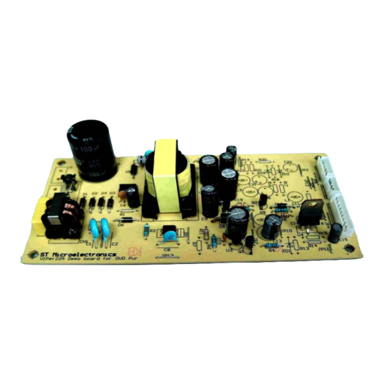
Figure 1. VIPer22A-E evaluation board
Table 1. Output specifications
Output 1
Output 2
5 V+/-5%
+12 V+/-5%
(1)
(1)
Imin.
Imax.
ac
20 mA
30 mA
ac
Imax.1.5 A
DocID10240 Rev 2
Application note
with the VIPer22A-E
®
Output 3
Output 4
-12 V+/-5%
-26 V+/-5%
(1)
(1)
Imax.
Imax.50 mA
30 mA
AN1897
family combine high voltage,
Output 5
Output 6
5 V
3.3 V+/-5%
stb
(1)
(1)
Imax.
Imax.100 mA
150 mA
Section 3.2
for cross-
www.st.com
+/-5%
1/17
17
Advertisement
Table of Contents

Related Manuals for ST VIPower VIPer22A-E


Summary of Contents for ST VIPower VIPer22A-E
- Page 1 DVD or VCD players. Generally, their power supply requires multiple outputs to supply a variety of control circuits: MCU, motor, amplifier, VFD. ® Offline switch mode power supply regulators from ST’s VIPer family combine high voltage, avalanche rugged vertical power MOSFET with current mode control PWM circuitry. The result is the innovative AC-DC converter, simpler, quicker, with reduced component count and cheap.
-
Page 2: Table Of Contents
Contents AN1897 Contents Application description and design ......3 Schematics ..........3 1.1.1 Start-up phase . -
Page 3: Application Description And Design
AN1897 Application description and design Application description and design Schematics The overall schematic is shown in Figure 1.1.1 Start-up phase The VIPer22A-E has an integrated high voltage current source linked to the drain pin. At the start-up converter, it charges the V capacitor until it reaches the start-up level (14.5 V), and the VIPer22A-E starts switching. -
Page 4: Primary Driver
Application description and design AN1897 Figure 2. VIPer22A-E FB pin internal structure 1.1.5 Primary driver In a flyback power supply, the transformer is used as an energy tank during the on-time of the MOSFET. When the MOSFET turns off, its drain voltage rises from a low value to the input voltage while the secondary diode conducts, transferring to the secondary side the magnetic energy stored in the transformer. - Page 5 AN1897 Application description and design Designing transformers for low leakage inductance involves several considerations: – Minimizing the number of turns – Keeping ratio of winding height to width small – Increasing width of windings – Minimizing the insulation between windings –...
- Page 6 Application description and design AN1897 Figure 3. Application schematic 6/17 DocID10240 Rev 2...
- Page 7 AN1897 Application description and design Figure 4. RCD clamp topology Figure 5. Zener clamp topology For safety requirements, a leakage inductance value is 1 to 3% of the open circuit primary inductance. A high efficiency transformer should have low inter-winding capacitance to decrease the switching losses.
-
Page 8: Layout Recommendation
Layout recommendation AN1897 Layout recommendation Since EMI issues are strongly related to layout, a basic rule has to be taken into account in high current path routing, (the current loop area has to be minimized). If a heatsink is used it has to be connected to ground to reduce common mode emissions, since it is close to the floating drain tab. -
Page 9: Experimental Results
AN1897 Experimental results Experimental results Efficiency Figure 7. Efficiency at 230 V (load on 5 V) Figure 8. Efficiency at 260 V (load on 5 V) Figure 9. Efficiency at 85 V (load on 5 V) Figure 10. Load regulation (load on + 5 V) DocID10240 Rev 2 9/17... -
Page 10: Regulation
Experimental results AN1897 Regulation Table 2. Line regulation Output 85 V 85 V 260 V 5 V/ 0.1 A 5.15 V 5.15 V 5.15 V / 0 A 5.15 V 5 15.15 V 5.15 V 12 V/ 0 A 12.08 V 12.11 V 12.12 V -12 V/ 0 A... - Page 11 AN1897 Experimental results Table 4. Full load regulation Output 85 V 230 V 260 V 5 V/ 1.5 A 5.02 V 5.09 V 5.08 V / 0 A 5.02 V 5.09 V 5.08 V 12 V/30 mA 12.03 V 12.06 V 12.05 V -12 V/30 mA -12.01 V...
-
Page 12: Transformer Specification
Transformer specification AN1897 Transformer specification Figure 12. Transformer structure Table 5. Winding parameters Wire size Layer description Symbol Start pin End pin Number of layers Turns (mm) Primary Pin 2 Pin 1 Out 1 (5 V/1.5 A) Pin 7 Pin 12 2*0.6 Out 2 (12 V/0.0 3 A) Pin 11... -
Page 13: Pcb Layout
AN1897 PCB layout PCB layout Figure 14. Bottom view of the evaluation board (not in scale) Figure 15. PCB art work (not in scale) DocID10240 Rev 2 13/17... - Page 14 PCB layout AN1897 Table 6. Bill of materials Reference Description Note Optocoupler PC817 Sharp VIPer22A-E DIP TL431 ACZ L4931 ABV33 SS9014 SS8550 D1, D2, D3, D4 1N4007 FR157 D6, D7, D9, D10, D13 STTH102 STPS5L60 D11, D12 1N5818 C1, C2 Y1 capacitor 2200 pF X2 capacitor 0.1 uF Electrolytic capacitor 100 uF/400 V...
- Page 15 AN1897 PCB layout Table 6. Bill of materials (continued) Reference Description Note Fuse 1 A J1, J2 2-pin connector 5-pin connector 4-pin connector 9-pin connector DocID10240 Rev 2 15/17...
-
Page 16: Revision History
Revision history AN1897 Revision history Table 7. Document revision history Date Revision Changes Updated the title in cover page. 12-Nov-2014 Content reworked to improve readability, no technical changes. 16/17 DocID10240 Rev 2... - Page 17 ST products and/or to this document at any time without notice. Purchasers should obtain the latest relevant information on ST products before placing orders. ST products are sold pursuant to ST’s terms and conditions of sale in place at the time of order acknowledgement.
Need help?
Do you have a question about the VIPower VIPer22A-E and is the answer not in the manual?
Questions and answers