
Related Manuals for Epson S1D13513


Summary of Contents for Epson S1D13513
- Page 1 S1D13513 Display Controller S5U13513P00C100 Evaluation Board User Manual Document Number: X78A-G-003-01.2 Rev. 1.2...
- Page 2 This evaluation board/kit or development tool is intended for use by an electronics engineer and is not a consumer product. The user should use it properly and in a safe manner. Seiko Epson does not assume any responsibility or liability of any kind of damage and/or fire caused by the use of it.
-
Page 3: Table Of Contents
4.1.3 S1D13513 Power ........13 Clocks ....... . . 14 Reset . - Page 4 Seiko Epson Corporation S5U13513P00C100 Evaluation Board Rev. 1.2...
-
Page 5: Introduction
Adapter board so that it can be used with a laptop or desktop computer, via USB 2.0. With some minor modifications, it is possible to connect the S5U13513P00C100 evaluation board to a Epson PC Card Extender board instead of a USB Adapter board. The S5U13513P00C100 evaluation board can also be used with many other native platforms via the host connectors which provide the appropriate signals to support a variety of CPUs. -
Page 6: Features
2 Features The S5U13513P00C100 Evaluation Board includes the following features: • 256-pin PBGA S1D13513 Display Controller • On-board SDRAM, selectable as 8MB x 32-bit or 8MB x 16-bit • Headers for connection to the S5U13U00P00C100 USB Adapter board or to the PC Card Extender board •... -
Page 7: Installation And Configuration
3.1 Configuration DIP Switch The S1D13513 has configuration inputs (CNF[8:0]) which are read on the rising edge of RESET#. A 10-position DIP switch (SW1) is used to configure the S1D13513 for multiple Host Bus Interfaces. - Page 8 Serial on HVDD2: Data valid on rising edge 11010b Reserved 11011b Reserved 11100b Reserved 11101b Reserved 11110b Reserved 11111b Reserved = Required settings when using S5U13U00P00C100 USB Adapter board (SW1-[9:1] = 101000000b) Seiko Epson Corporation S5U13513P00C100 Evaluation Board Rev. 1.2...
- Page 9 SH4 Little Endian: Active High WAIT# with tri-state 11011b Reserved 11100b SH3 Big Endian: Active Low WAIT# with tri-state 11101b SH3 Big Endian: Active Low WAIT# always driven 11110b SH4 Big Endian: Active High WAIT# with tri-state 11111b Reserved Seiko Epson Corporation S5U13513P00C100 Evaluation Board Rev. 1.2...
-
Page 10: Configuration Jumpers
— measurement HVDD3 current HVDD3 Normal — measurement HVDD4 current HVDD4 Normal — measurement HVDD5 current JP10 HVDD5 Normal — measurement JP11 SDRAM Width Select 32-bit wide SDRAM 16-bit wide SDRAM — Seiko Epson Corporation S5U13513P00C100 Evaluation Board Rev. 1.2... - Page 11 Installation and Configuration JP1-JP10 - Power Supplies for the S1D13513 JP1-JP10 can be used to measure current consumption of each S1D13513 power supply. When the jumper is at position 1-2, normal operation is selected. When no jumper is installed, the current consumption for each power supply can be measured by connecting an ammeter to pin 1 and 2 of the jumper.
- Page 12 When the jumper is at position 2-3, the external SDRAM is 16-bit wide and memory size is 16MB. In this position one memory chip is disabled and only one chip is active (16MB and 16-bit wide). JP11 Figure 3-3: Configuration Jumper Location (JP11) Seiko Epson Corporation S5U13513P00C100 Evaluation Board Rev. 1.2...
-
Page 13: Technical Description
LED backlight on some LCD panels. 4.1.3 S1D13513 Power The S1D13513 Display Controller requires 1.8V and 3.3V power supplies. 1.8V power is provided by the on-board linear voltage regulator. It is used for CoreVDD, PLLVDD1, PLLVDD2, OSCVDD1, OSCVDD2. -
Page 14: Clocks
(see H2 connector or P1 connector). The reset signal will reset the S1D13513 Display Controller and is available on the H6 and H7 connectors. It is possible to remove the reset signal from the H6 and H7 connectors by removing the 0 Ohm resistor R80 from the board. -
Page 15: Host Interface
S5U13513P00C100. 4.4.2 Connecting to the Epson PC Card Extender Board The S5U13513P00C100 evaluation board may be connected to an Epson PC Card Extender Board, but it will require an external 3.3V power supply and some modifications to the S5U13513P00C100 board. -
Page 16: Direct Host Bus Interface Support
S1D13513 pin mapping, refer to the S1D13513 Hardware Functional Specification, document number X78B-A-001-xx. All S1D13513 host interface pins are available on connectors H2 and H3 which allow the S5U13513P00C100 to be connected to a variety of development platforms. However, connectors H2 and H3 are not populated on the S5U13513P00C100 evaluation board. -
Page 17: Lcd Panel Interface
The LCD interface signals are available on connectors H4 and H5. Connector H5 includes GPIOG[4:0] which may be used as additional signals for extended TFT interfaces. For S1D13513 LCD interface pin mapping, refer to the S1D13513 Hardware Functional Speci- fication, document number X78B-A-001-xx. -
Page 18: Camera Interface
Connector H6 and H7 may be used to evaluate any function for which the GPIOA[7:0], GPIOB[7:0], GPIOC[7:0], GPIOD[3:0] can be configured. The S1D13513 has an I2C interface which uses two signals that are connected to both the H6 and H7 connectors. The default configuration of the evaluation board has the I2C signals, I2C_SCL and I2C_SDA, pulled high to CIOVDD1. -
Page 19: Yuv Output For Tv Display
Technical Description 4.7 YUV Output for TV Display The S1D13513 can output YUV data which can be used to display an image on a TV screen via an external video encoder. The YUV output is multiplexed with other functions on the GPIOC[7:0] and GPIOD[2:0] pins. -
Page 20: Jtag Connector
Technical Description 4.11 JTAG Connector The S1D13513 design includes a JTAG interface. All the JTAG signals are available on connector H1, however, connector H1 is not populated on the board. For the pinout of connector H1, see “Schematic Diagrams” on page 24. -
Page 21: Parts List
Micro Commercial Co. MBR0530 MBR0530-TP FILTER 3-TERM 60MHZ F1, F2 ACF451832-222 TDK ACF451832-222 300MA SMD HEADER 6X2 Samtec TSW-106-05-G-D H2, H3 HEADER_17X2 AMP 1-87215-7 LCD Connector Samtec TST-120-01-G-D Extended LCD Connector Samtec TST-120-01-G-D Seiko Epson Corporation S5U13513P00C100 Evaluation Board Rev. 1.2... - Page 22 887k 1% R104 Panasonic - ECG EVN- R106 200k 5ESX50B25 SH1, SH2, SH3, SH4, Sullins Electronics Corp. SH5, SH6, SH7, SH8, .100 in. Jumper Shunt JUMPER SHORTING TIN STC02SYAN SH9, SH10, SH11 Seiko Epson Corporation S5U13513P00C100 Evaluation Board Rev. 1.2...
- Page 23 ITT Industries SW TACT-SPST PLT GULLWING KSC241GLFS TPGND1, TPGND2, PC TEST POINT TP_SMT Keystone 5015 TPGND3, TP3.3VDD1 MINIATURE SMT TP SIP S1D13513 PBGA256 alternate Micron U2, U3 IS42S16800D-7TL ISSI IS42S16800D-7TL MT48LC8M16A2P-7E IC 2.64V SUPPLY MON Texas Instruments TPS3801L30DCKR SOT-323-5 TPS3801L30DCKR Alternate MIC39100- MIC37100-1.8WS...
-
Page 24: Schematic Diagrams
Schematic Diagrams 6 Schematic Diagrams Figure 6-1: S5U13513P00C100 Schematics (1 of 4) Seiko Epson Corporation S5U13513P00C100 Evaluation Board Rev. 1.2... - Page 25 SDRAM 2Mb x 16-bit x 4 2Mb x 16-bit x 4 2Mb x 16-bit x 4 2Mb x 16-bit x 4 banks banks banks banks Figure 6-2: S5U13513P00C100 Schematics (2 of 4) Seiko Epson Corporation S5U13513P00C100 Evaluation Board Rev. 1.2...
- Page 26 Schematic Diagrams Figure 6-3: S5U13513P00C100 Schematics (3 of 4) Seiko Epson Corporation S5U13513P00C100 Evaluation Board Rev. 1.2...
- Page 27 Schematic Diagrams Figure 6-4: S5U13513P00C100 Schematics (4 of 4) Seiko Epson Corporation S5U13513P00C100 Evaluation Board Rev. 1.2...
-
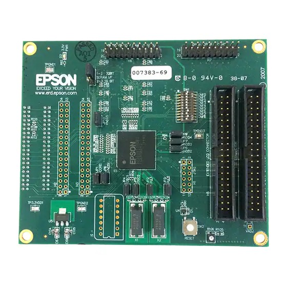
Page 28: S5U13513P00C100 Board Layout
S5U13513P00C100 Board Layout 7 S5U13513P00C100 Board Layout Figure 7-1: S5U13513P00C100 Board Layout - Top View Seiko Epson Corporation S5U13513P00C100 Evaluation Board Rev. 1.2... - Page 29 S5U13513P00C100 Board Layout Figure 7-2: S5U13513P00C100 Board Layout - Bottom View Seiko Epson Corporation S5U13513P00C100 Evaluation Board Rev. 1.2...
-
Page 30: Change Record
• updated parts list • added board layout X78A-G-003-00 Revision 0.02 • revised manual due to design changes • added new schematics • added new parts list X78A-G-003-00 Revision 0.01 • Initial draft of manual Seiko Epson Corporation S5U13513P00C100 Evaluation Board Rev. 1.2... -
Page 31: Sales And Technical Support
Sales and Technical Support 9 Sales and Technical Support For more information on Epson Display Controllers, visit the Epson Global website. https://global.epson.com/products_and_drivers/semicon/products/display_controllers/ For Sales and Technical Support, contact the Epson representative for your region. https://global.epson.com/products_and_drivers/semicon/information/support.html Seiko Epson Corporation S5U13513P00C100 Evaluation Board...