
Related Manuals for Casio SF-7900E


Summary of Contents for Casio SF-7900E
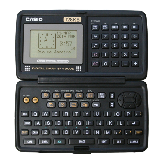
- Page 1 (without price) (with price) SF-7900E (LX-552A) SF-8900 (LX-552I/J) JAN. 1995 SF-7900E...
-
Page 2: Table Of Contents
CONTENTS SPECIFICATIONS ........................ 1 TO REPLACE THE BATTERY ..................... 2 TO CHECK THE MEMORY CAPACITY ................2 ERROR MESSAGE ....................... 3 TO RESET THE SF UNIT'S MEMORY ................. 4 TO SAVE THE DATA TO ANOTHER UNIT ................. 5 BLOCK DIAGRAM ........................ 8 CIRCUIT EXPLANATIONS System chart ......................... -
Page 3: Specifications
24-digit approximations; date calcula- tions; other mixed calculations General: 16-column × 8-line LCD Display element: Memory capacity: SF-7900E: 128KB (103436 bytes) SF-8900: 256KB (234508 bytes) Main component: Power supply: 3 lithium batteries (CR2032) Power consumption: 0.07 W... -
Page 4: To Replace The Battery
TO REPLACE THE BATTERY To replace the batteries Loosen the screw on the back of the SF unit that holds the battery compartment cover in place, and remove the cover. Caution In the next step, be sure to remove only one battery at a time. Screw Otherwise, you will lose all data stored in memory. -
Page 5: Error Message
ERROR MESSAGE Message Meaning Action DATA ITEM Search operation Current search operation NOT FOUND! attempted when no data cannot be performed. NO DATA is stored in memory. IN MEMORY! DATA ITEM Data specified in search Change specification or NOT FOUND! operation does not exist cancel search. -
Page 6: To Reset The Sf Unit's Memory
TO RESET THE SF UNIT'S MEMORY The following procedure erases all data stored in the memory of the SF unit. Perform the following operation only when you want to delete all data and initialize the settings of the SF unit. Remember –... -
Page 7: To Save The Data To Another Unit
TO SAVE THE DATA TO ANOTHER UNIT SF-7900 can transfer customers data to another SF-7900 with memory protection only when replacing the LCD or the outer case. How to transfer the data * Before connecting the cable (SB-60 or SB-62), be sure to reset the slave unit to clear all data. - Page 8 5) Set up the slave unit. While in the Calendar Display, Telephone Directory, Business Card Library, Memo Mode, or Schedule Keeper, press the FUNCTION key followed by 4 to select " DATA COMM", and the following menu appears. 1 SEND FUNCTION 2 RECEIVE 3 PRINT...
- Page 9 Press 3 to select "ALL DATA". The following display appears to confirm if you wish to proceed. SEND ALL DATA ITEM ? SET / ESC Press the SET key to proceed with the data transmission, or press ESC if you wish to cancel.
-
Page 10: Block Diagram
PCB-L552-1(SF-8900) HD62076C03 LSI1 OPEN (OFF) LOCK (ON) MAIN SWITCH (Operation Program) LSI5 Power supply circuit MSM51008AFP-10LL LSI3, LSI4 SF-7900E: RAM × 1 SF-8900: RAM × 2 GATE ARRAY SSC2571 LSI2 INTERFACE FOR DATA TRANSMISSION & DATA RECEPTION — 8 —... - Page 11 CIRCUIT EXPLANATIONS System chart The circuitry operates in the following order: Low battery detector Gate array Power supply circuit (Pin24) (Pin28) V1~V5 for LCD (Pin49) (Pin62) (Pin35) (Pin58) "L" "L" "L" "L" "H" 2 MHz (Pin41) (Pin45) (Pin40) V2ON OSCI OSCO (Pin70) VDD1...
- Page 12 Power supply circuit Power supply circuit for CPU, GATE ARRAY and RAMs. When the main batteries are set, the voltage (9V) is applied to the terminal VDD1 of CPU (LSI1), GATE ARRAY (LSI2) and RAM (LSI4). When IC2 receives the voltage, it provides 4V to the GND lines from the terminal OUT (Pin No.1). Main switch The CPU (LSI1) detects the informations of the Main switch by the terminal SW (Pin No.36) from the SWO signal of the GATE ARRAY (LSI2).
- Page 13 Main switch and power on switch from IC4 (Pin35) MAIN SWITCH (Pin36) GATE ARRAY "L" (Pin62) "L" OSCI HD62076C03 2 MHz (Pin26) OSCO (Pin54) (Pin53) 4S66F "H" "L" POWER ON SWITCH When the main switch is set to on position, SW terminal of CPU receives "L", then KAC terminal will be "L"...
-
Page 14: Cpu Pin Description (Hd62076C03)
CPU pin description (HD62076C03) Pin No. Name In/Out Status Status Description of OFF of ON 1~14,16,17 A0~A15 Pulse Address Bus line 15,39, 100 GND terminal Pulse Write signal Pulse Read signal Pulse Chip select signal for Gate array Chip select signal Chip select signal Pulse Chip select signal... -
Page 15: Gate Array Pin Descriptions (Ssc2571F0A)
Gate array pin descriptions (SSC2571F0A): Used in SF-7900E Pin No. Name In/Out Description VSS1 GND terminal Clock out Clock in 6V input 5~10 A0~3,A14,15 Address input Chip select signal from CPU Chip select signal from CPU Chip select signal from CPU... -
Page 16: Gate Array Pin Descriptions (Ssc2571F0B)
Pin No. Name In/Out Description Not used Output enable for ROM Buzzer signal Connected to GND Buzzer signal Main switch control signal VH4(VCC) 9V input Transmission data output terminal Gate array pin descriptions (SSC2571F0B): Used in SF-8900 Pin No. Name In/Out Description VSS1... -
Page 17: Operation Program Rom Pin Descriptions
Pin No. Name In/Out Description RA20 Not used Address bus VSS(GND) GND terminal VH3(VCC) 9V input 6V input Address bus Address bus Chip enable signal for ROM (Not used) Chip select signal for RAM (Not used) Chip select signal Not used Not used Chip select signal Buzzer signal... -
Page 18: Diagnostic Operation
After this operation, the machine will beep and display "SELF-TEST". QUIT BY OFF CASIO 1993. 11. 09 The menu appears after pressing SET key. Tests are con- MENU TOP SHEET ducted by selecting the mode from the list on screen. The 1 : DISP CHECK each test can be selected by numeral keys. - Page 19 RAM and displays the 3 : PAT. CHANGE results. PAT. CHANGE : Change the test data pattern. CASIO 1993. 11. 09 #1---Test data pattern(00,01,02...) #2---Test data pattern(FF,FE,FD..) 1) RAM write The unit will beep after a second.
- Page 20 2 : SPECIFIC ADDR address. 3 : TIME DISPLAY TIME DISPLAY : Bring up clock display. The present time, date and daily alarm can be set. CASIO 1993. 11. 09 1) Check sum Time display CHECKSUM CALC TIME DISPLAY 1990-03-00 C0 O...
- Page 21 1 key : Transmission mode. The data of trans- mission is "H" and it is sent out by the data of H34 and H38 by the Xon/Xoff control. CASIO 1993.11.09 2 key : Reception mode. Make sure to set the Parameter parameter to match that of the transitting side.
- Page 22 LOOP BACK LOOP BACK NOW EXECUTING! COMPLETE! CASIO 1993. 11. 09 CASIO 1993. 11. 09 Break display (Broken transmission) Error display TRANS BREAK! TRANS ERROR! CASIO 1993. 11. 09 CASIO 1993. 11. 09 7. Others 1) When power is off after presetting an alarm time, the unit automatically powered on at the alarm time.
-
Page 23: Troubleshooting
TROUBLESHOOTING Before the following solutions will be done, save data if possible. SYMPTOM CAUSE SOLUTION No power Battery shortage Replace batteries Poor soldering of the power supply Resolder circuit Defective LSI-1 or LSI-2 Replace it No display at all or wrong Defective TAB LSI Replace it display... -
Page 24: Schematic Diagram
SCHEMATIC DIAGRAM Main PCB: SF-7900E R22 R27 R28 R29 — — S-80766AH Note: The following parts are not mounted. — — — RH5VA60BA C16, R24 — 23 —... - Page 25 Main PCB: SF8900 — 24 —...
-
Page 26: Display Pcb
Display PCB — 25 —... -
Page 27: Key Matrix (Display Side)
Key Matrix — 26 —... - Page 28 Key Matrix (Display side) — 27 —...
-
Page 29: Parts List
AT : SF-7900E IT : SF-8900 PARTS LIST JT : SF-8900 (B.O.S.S.) FOB Japan Item Code No. Parts Name Specification Quantity N.R.Yen AT IT JT Unit Price CPU BOARD ASS'Y 2803 6813 Capapcitor CB0011341R3 1 20 2845 2289 Chip capacitor... - Page 30 FOB Japan Item Code No. Parts Name Specification Quantity N.R.Yen AT IT JT Unit Price COMPONENT 3335 5257 LCD CD791-TS 6411 6340 Heat seal FX20P320003 6512 1280 Haet seal FX200P80074 1 10 6512 1230 Heat seal FX200P60014 6512 1240 Protection tape HGFC0007409 1 20 6411 8470 Protection tape...
-
Page 31: Assembly View
ASSEMBLY VIEW — 31 —... - Page 32 MA0400751A...