Sign In
Upload
Manuals
Brands
ST Manuals
Computer Hardware
STM32F4 Series
ST STM32F4 Series Manuals
Manuals and User Guides for ST STM32F4 Series. We have
8
ST STM32F4 Series manuals available for free PDF download: Programming Manual, Application Note, Getting Started, User Manual, Manual
ST STM32F4 Series Programming Manual (260 pages)
Cortex-M4
Brand:
ST
| Category:
Computer Hardware
| Size: 3.48 MB
Table of Contents
Reference Documents
1
Table of Contents
2
About this Document
12
Typographical Conventions
12
List of Abbreviations for Registers
12
About the STM32 Cortex-M4 Processor and Core Peripherals
13
Figure 1. STM32 Cortex-M4 Implementation
13
Cortex-M4 Processor Features and Benefits Summary
14
Integrated Configurable Debug
14
System Level Interface
14
Cortex-M4 Core Peripherals
15
The Cortex-M4 Processor
16
Programmers Model
16
Processor Mode and Privilege Levels for Software Execution
16
Stacks
16
Core Registers
17
Figure 2. Processor Core Registers
17
Table 1. Summary of Processor Mode, Execution Privilege Level, and Stack Usage
17
Table 2. Core Register Set Summary
17
Program Counter
18
Program Status Register
18
Stack Pointer
18
Table 3. PSR Register Combinations
19
Figure 3. APSR, IPSR and EPSR Bit Assignments
19
Figure 4. PSR Bit Assignments
19
Table 4. APSR Bit Definitions
20
Table 5. IPSR Bit Definitions
21
Table 6. EPSR Bit Definitions
22
Table 7. PRIMASK Register Bit Definitions
23
Table 8. FAULTMASK Register Bit Definitions
23
Figure 5. PRIMASK Bit Assignments
23
Figure 6. FAULTMASK Bit Assignments
23
Table 9. BASEPRI Register Bit Assignments
24
Table 10. CONTROL Register Bit Definitions
24
Figure 7. BASEPRI Bit Assignments
24
Exceptions and Interrupts
25
Data Types
25
The Cortex Microcontroller Software Interface Standard (CMSIS)
25
Memory Model
27
Figure 8. Memory Map
27
Memory Regions, Types and Attributes
28
Memory System Ordering of Memory Accesses
28
Table 11. Ordering of Memory Accesses
28
Behavior of Memory Accesses
29
Table 12. Memory Access Behavior
29
Software Ordering of Memory Accesses
30
Bit-Banding
31
Table 13. SRAM Memory Bit-Banding Regions
31
Table 14. Peripheral Memory Bit-Banding Regions
31
Figure 9. Bit-Band Mapping
32
Figure 10. Little-Endian Example
33
Memory Endianness
33
Synchronization Primitives
33
Programming Hints for the Synchronization Primitives
35
Table 15. CMSIS Functions for Exclusive Access Instructions
35
Exception Model
36
Exception States
36
Exception Types
36
Table 16. Properties of the Different Exception Types
37
Exception Handlers
38
Vector Table
39
Figure 11. Vector Table
39
Exception Priorities
40
Interrupt Priority Grouping
40
Exception Entry and Return
41
Figure 12. Cortex-M4 Stack Frame Layout
42
Fault Handling
43
Table 17. Exception Return Behavior
43
Fault Types
44
Table 18. Faults
44
Fault Escalation and Hard Faults
45
Fault Status Registers and Fault Address Registers
46
Lockup
46
Power Management
46
Table 19. Fault Status and Fault Address Registers
46
Entering Sleep Mode
47
Wakeup from Sleep Mode
47
External Event Input / Extended Interrupt and Event Input
48
Power Management Programming Hints
48
The STM32 Cortex-M4 Instruction Set
49
Instruction Set Summary
49
Table 20. Cortex-M4 Instructions
49
CMSIS Intrinsic Functions
57
Table 21. CMSIS Intrinsic Functions to Generate some Cortex-M4 Instructions
58
Table 22. CMSIS Intrinsic Functions to Access the Special Registers
58
About the Instruction Descriptions
59
Operands
59
Restrictions When Using PC or SP
59
Flexible Second Operand
59
Shift Operations
61
Figure 13. ASR #3
61
Figure 14. LSR #3
62
Figure 15. LSL #3
62
Figure 16. ROR #3
63
Figure 17. RRX #3
63
Address Alignment
64
PC-Relative Expressions
64
Conditional Execution
64
Table 23. Condition Code Suffixes
66
Instruction Width Selection
67
Memory Access Instructions
68
Table 24. Memory Access Instructions
68
Adr
69
LDR and STR, Immediate Offset
70
Table 25. Immediate, Pre-Indexed and Post-Indexed Offset Ranges
71
LDR and STR, Register Offset
72
LDR and STR, Unprivileged
73
LDR, PC-Relative
74
Table 26. Label-PC Offset Ranges
74
LDM and STM
75
PUSH and POP
77
LDREX and STREX
78
Clrex
79
General Data Processing Instructions
80
Table 27. Data Processing Instructions
80
ADD, ADC, SUB, SBC, and RSB
82
AND, ORR, EOR, BIC, and ORN
84
ASR, LSL, LSR, ROR, and RRX
85
Clz
86
CMP and CMN
87
MOV and MVN
88
Movt
90
REV, REV16, REVSH, and RBIT
91
SADD16 and SADD8
92
SHADD16 and SHADD8
93
SHASX and SHSAX
94
SHSUB16 and SHSUB8
95
SSUB16 and SSUB8
96
SASX and SSAX
97
TST and TEQ
98
UADD16 and UADD8
99
UASX and USAX
100
UHADD16 and UHADD8
101
UHASX and UHSAX
102
UHSUB16 and UHSUB8
103
Sel
104
Usad8
105
Usada8
106
USUB16 and USUB8
107
Multiply and Divide Instructions
108
Table 28. Multiply and Divide Instructions
108
MUL, MLA, and MLS
109
UMULL, UMAAL and UMLAL
110
SMLA and SMLAW
111
Smlad
113
SMLAL and SMLALD
114
SMLSD and SMLSLD
116
SMMLA and SMMLS
118
Smmul
119
SMUAD and SMUSD
120
SMUL and SMULW
121
UMULL, UMLAL, SMULL, and SMLAL
122
SDIV and UDIV
123
Saturating Instructions
124
Table 29. Saturating Instructions
124
SSAT and USAT
125
SSAT16 and USAT16
126
QADD and QSUB
127
QASX and QSAX
128
QDADD and QDSUB
129
UQASX and UQSAX
130
UQADD and UQSUB
131
Packing and Unpacking Instructions
133
Table 30. Packing and Unpacking Instructions
133
PKHBT and PKHTB
134
SXT and UXT
135
SXTA and UXTA
136
Bitfield Instructions
137
Table 31. Instructions that Operate on Adjacent Sets of Bits
137
BFC and BFI
138
SBFX and UBFX
139
SXT and UXT
140
B, BL, BX, and BLX
141
Branch and Control Instructions
141
Table 32. Branch and Control Instructions
141
Table 33. Branch Ranges
142
CBZ and CBNZ
143
TBB and TBH
146
Floating-Point Instructions
148
Table 34. Floating-Point Instructions
148
Vabs
150
Vadd
151
Vcmp, Vcmpe
152
VCVT, VCVTR between Floating-Point and Integer
153
VCVT between Floating-Point and Fixed-Point
154
Vcvtb, Vcvtt
155
VDIV
156
Vfma, Vfms
157
Vfnma, Vfnms
158
Vldm
159
Vldr
160
Vlma, Vlms
161
VMOV Immediate
162
VMOV Register
163
VMOV Scalar to ARM Core Register
164
VMOV ARM Core Register to Single Precision
165
VMOV Two ARM Core Registers to Two Single Precision
166
VMOV ARM Core Register to Scalar
167
Vmrs
168
Vmsr
169
Vmul
170
Vneg
171
Vnmla, Vnmls, Vnmul
172
Vpop
173
Vpush
174
Vsqrt
175
Vstm
176
Vstr
177
Vsub
178
Miscellaneous Instructions
179
Table 35. Miscellaneous Instructions
179
Bkpt
180
Cps
181
Dmb
182
Dsb
183
Isb
184
Mrs
185
Msr
186
Nop
187
Sev
188
Svc
189
Wfe
190
Wfi
191
Advertisement
ST STM32F4 Series Programming Manual (262 pages)
Brand:
ST
| Category:
Computer Hardware
| Size: 2.73 MB
Table of Contents
Table 1. Applicable Products
1
Table of Contents
2
About this Document
12
Typographical Conventions
12
List of Abbreviations for Registers
12
About the STM32 Cortex-M4 Processor and Core Peripherals
13
Figure 1. STM32 Cortex-M4 Implementation
13
Integrated Configurable Debug
14
System Level Interface
14
Cortex-M4 Processor Features and Benefits Summary
15
Cortex-M4 Core Peripherals
16
The Cortex-M4 Processor
17
Programmers Model
17
Processor Mode and Privilege Levels for Software Execution
17
Stacks
17
Core Registers
18
Table 2. Summary of Processor Mode, Execution Privilege Level, and Stack Usage
18
Table 3. Core Register Set Summary
18
Figure 2. Processor Core Registers
18
Table 4. PSR Register Combinations
20
Figure 3. APSR, IPSR and EPSR Bit Assignment
20
Figure 4. PSR Bit Assignment
20
Table 5. APSR Bit Definitions
21
Table 6. IPSR Bit Definitions
22
Table 7. EPSR Bit Definitions
23
Table 8. PRIMASK Register Bit Definitions
24
Table 9. FAULTMASK Register Bit Definitions
24
Figure 5. PRIMASK Bit Assignment
24
Figure 6. FAULTMASK Bit Assignment
24
Table 10. BASEPRI Register Bit Assignment
25
Table 11. CONTROL Register Bit Definitions
25
Figure 7. BASEPRI Bit Assignment
25
Exceptions and Interrupts
26
Data Types
26
The Cortex Microcontroller Software Interface Standard (CMSIS)
26
Memory Model
28
Figure 8. Memory Map
28
Memory Regions, Types and Attributes
29
Memory System Ordering of Memory Accesses
29
Table 12. Ordering of Memory Accesses
29
Behavior of Memory Accesses
30
Table 13. Memory Access Behavior
30
Software Ordering of Memory Accesses
31
Bit-Banding
32
Table 14. SRAM Memory Bit-Banding Regions
32
Table 15. Peripheral Memory Bit-Banding Regions
32
Figure 9. Bit-Band Mapping
33
Figure 10. Little-Endian Example
34
Memory Endianness
34
Synchronization Primitives
34
Programming Hints for the Synchronization Primitives
36
Table 16. CMSIS Functions for Exclusive Access Instructions
36
Exception Model
37
Exception States
37
Exception Types
37
Table 17. Properties of the Different Exception Types
38
Exception Handlers
39
Vector Table
40
Figure 11. Vector Table
40
Exception Priorities
41
Interrupt Priority Grouping
41
Exception Entry and Return
42
Figure 12. Cortex-M4 Stack Frame Layout
43
Fault Handling
44
Table 18. Exception Return Behavior
44
Fault Types
45
Table 19. Faults
45
Fault Escalation and Hard Faults
46
Fault Status Registers and Fault Address Registers
47
Lockup
47
Power Management
47
Table 20. Fault Status and Fault Address Registers
47
Entering Sleep Mode
48
Wakeup from Sleep Mode
48
External Event Input / Extended Interrupt and Event Input
49
Power Management Programming Hints
49
The STM32 Cortex-M4 Instruction Set
50
Instruction Set Summary
50
Table 21. Cortex-M4 Instructions
50
CMSIS Intrinsic Functions
58
Table 22. CMSIS Intrinsic Functions to Generate some Cortex-M4 Instructions
59
Table 23. CMSIS Intrinsic Functions to Access the Special Registers
59
About the Instruction Descriptions
60
Operands
60
Restrictions When Using PC or SP
60
Flexible Second Operand
60
Shift Operations
62
Figure 13. ASR #3
62
Figure 14. LSR #3
63
Figure 15. LSL #3
63
Figure 16. ROR #3
64
Figure 17. RRX #3
64
Address Alignment
65
PC-Relative Expressions
65
Conditional Execution
65
Table 24. Condition Code Suffixes
67
Instruction Width Selection
68
Memory Access Instructions
69
Table 25. Memory Access Instructions
69
Adr
70
LDR and STR, Immediate Offset
71
Table 26. Immediate, Pre-Indexed and Post-Indexed Offset Ranges
72
LDR and STR, Register Offset
73
LDR and STR, Unprivileged
74
LDR, PC-Relative
75
Table 27. Label-PC Offset Ranges
75
LDM and STM
76
PUSH and POP
78
LDREX and STREX
79
Clrex
80
General Data Processing Instructions
81
Table 28. Data Processing Instructions
81
ADD, ADC, SUB, SBC, and RSB
83
AND, ORR, EOR, BIC, and ORN
85
ASR, LSL, LSR, ROR, and RRX
86
Clz
87
CMP and CMN
88
MOV and MVN
89
Movt
91
REV, REV16, REVSH, and RBIT
92
SADD16 and SADD8
93
SHADD16 and SHADD8
94
SHASX and SHSAX
95
SHSUB16 and SHSUB8
96
SSUB16 and SSUB8
97
SASX and SSAX
98
TST and TEQ
99
UADD16 and UADD8
100
UASX and USAX
101
UHADD16 and UHADD8
102
UHASX and UHSAX
103
UHSUB16 and UHSUB8
104
Sel
105
Usad8
106
Usada8
107
USUB16 and USUB8
108
Multiply and Divide Instructions
109
Table 29. Multiply and Divide Instructions
109
MUL, MLA, and MLS
110
UMULL, UMAAL and UMLAL
111
SMLA and SMLAW
112
Smlad
114
SMLAL and SMLALD
115
SMLSD and SMLSLD
117
SMMLA and SMMLS
119
Smmul
120
SMUAD and SMUSD
121
SMUL and SMULW
122
UMULL, UMLAL, SMULL, and SMLAL
123
SDIV and UDIV
124
Saturating Instructions
125
Table 30. Saturating Instructions
125
SSAT and USAT
126
SSAT16 and USAT16
127
QADD and QSUB
128
QASX and QSAX
129
QDADD and QDSUB
130
UQASX and UQSAX
131
UQADD and UQSUB
132
Packing and Unpacking Instructions
134
Table 31. Packing and Unpacking Instructions
134
PKHBT and PKHTB
135
SXT and UXT
136
SXTA and UXTA
137
Bitfield Instructions
138
Table 32. Instructions that Operate on Adjacent Sets of Bits
138
BFC and BFI
139
SBFX and UBFX
140
SXT and UXT
141
B, BL, BX, and BLX
142
Branch and Control Instructions
142
Table 33. Branch and Control Instructions
142
Table 34. Branch Ranges
143
CBZ and CBNZ
144
TBB and TBH
147
Floating-Point Instructions
149
Table 35. Floating-Point Instructions
149
Vabs
151
Vadd
152
Vcmp, Vcmpe
153
VCVT, VCVTR between Floating-Point and Integer
154
VCVT between Floating-Point and Fixed-Point
155
Vcvtb, Vcvtt
156
VDIV
157
Vfma, Vfms
158
Vfnma, Vfnms
159
Vldm
160
Vldr
161
Vlma, Vlms
162
VMOV Immediate
163
VMOV Register
164
VMOV Scalar to Arm Core Register
165
VMOV Arm Core Register to Single Precision
166
VMOV Two Arm Core Registers to Two Single Precision
167
VMOV Arm Core Register to Scalar
168
Vmrs
169
Vmsr
170
Vmul
171
Vneg
172
Vnmla, Vnmls, Vnmul
173
Vpop
174
Vpush
175
Vsqrt
176
Vstm
177
Vstr
178
Vsub
179
Miscellaneous Instructions
180
Table 36. Miscellaneous Instructions
180
Bkpt
181
Cps
182
Dmb
183
Dsb
184
Isb
185
Mrs
186
Msr
187
Nop
188
Sev
189
Svc
190
Wfe
191
Wfi
192
ST STM32F4 Series Programming Manual (262 pages)
Brand:
ST
| Category:
Computer Hardware
| Size: 2.72 MB
Table of Contents
Table 1. Applicable Products
1
Table of Contents
2
About this Document
12
Typographical Conventions
12
List of Abbreviations for Registers
12
About the STM32 Cortex-M4 Processor and Core Peripherals
13
Figure 1. STM32 Cortex-M4 Implementation
13
System Level Interface
14
Integrated Configurable Debug
14
Cortex-M4 Processor Features and Benefits Summary
15
Cortex-M4 Core Peripherals
16
The Cortex-M4 Processor
17
Programmers Model
17
Processor Mode and Privilege Levels for Software Execution
17
Stacks
17
Core Registers
18
Table 2. Summary of Processor Mode, Execution Privilege Level, and Stack Usage
18
Table 3. Core Register Set Summary
18
Figure 2. Processor Core Registers
18
Table 4. PSR Register Combinations
20
Figure 3. APSR, IPSR and EPSR Bit Assignment
20
Figure 4. PSR Bit Assignment
20
Table 5. APSR Bit Definitions
21
Table 6. IPSR Bit Definitions
22
Table 7. EPSR Bit Definitions
23
Table 8. PRIMASK Register Bit Definitions
24
Table 9. FAULTMASK Register Bit Definitions
24
Figure 5. PRIMASK Bit Assignment
24
Figure 6. FAULTMASK Bit Assignment
24
Table 10. BASEPRI Register Bit Assignment
25
Table 11. CONTROL Register Bit Definitions
25
Figure 7. BASEPRI Bit Assignment
25
Exceptions and Interrupts
26
Data Types
26
The Cortex Microcontroller Software Interface Standard (CMSIS)
26
Memory Model
28
Figure 8. Memory Map
28
Memory Regions, Types and Attributes
29
Memory System Ordering of Memory Accesses
29
Table 12. Ordering of Memory Accesses
29
Behavior of Memory Accesses
30
Table 13. Memory Access Behavior
30
Software Ordering of Memory Accesses
31
Bit-Banding
32
Table 14. SRAM Memory Bit-Banding Regions
32
Table 15. Peripheral Memory Bit-Banding Regions
32
Figure 9. Bit-Band Mapping
33
Memory Endianness
34
Synchronization Primitives
34
Figure 10. Little-Endian Example
34
Programming Hints for the Synchronization Primitives
36
Table 16. CMSIS Functions for Exclusive Access Instructions
36
Exception Model
37
Exception States
37
Exception Types
37
Table 17. Properties of the Different Exception Types
38
Exception Handlers
39
Vector Table
40
Figure 11. Vector Table
40
Exception Priorities
41
Interrupt Priority Grouping
41
Exception Entry and Return
42
Figure 12. Cortex-M4 Stack Frame Layout
43
Fault Handling
44
Table 18. Exception Return Behavior
44
Fault Types
45
Table 19. Faults
45
Fault Escalation and Hard Faults
46
Fault Status Registers and Fault Address Registers
47
Lockup
47
Power Management
47
Table 20. Fault Status and Fault Address Registers
47
Entering Sleep Mode
48
Wakeup from Sleep Mode
48
External Event Input / Extended Interrupt and Event Input
49
Power Management Programming Hints
49
The STM32 Cortex-M4 Instruction Set
50
Instruction Set Summary
50
Table 21. Cortex-M4 Instructions
50
CMSIS Intrinsic Functions
58
Table 22. CMSIS Intrinsic Functions to Generate some Cortex-M4 Instructions
59
Table 23. CMSIS Intrinsic Functions to Access the Special Registers
59
About the Instruction Descriptions
60
Operands
60
Restrictions When Using PC or SP
60
Flexible Second Operand
60
Shift Operations
62
Figure 13. ASR #3
62
Figure 14. LSR #3
63
Figure 15. LSL #3
63
Figure 16. ROR #3
64
Figure 17. RRX #3
64
Address Alignment
65
PC-Relative Expressions
65
Conditional Execution
65
Table 24. Condition Code Suffixes
67
Instruction Width Selection
68
Memory Access Instructions
69
Table 25. Memory Access Instructions
69
Adr
70
LDR and STR, Immediate Offset
71
Table 26. Immediate, Pre-Indexed and Post-Indexed Offset Ranges
72
LDR and STR, Register Offset
73
LDR and STR, Unprivileged
74
LDR, PC-Relative
75
Table 27. Label-PC Offset Ranges
75
LDM and STM
76
PUSH and POP
78
LDREX and STREX
79
Clrex
80
General Data Processing Instructions
81
Table 28. Data Processing Instructions
81
ADD, ADC, SUB, SBC, and RSB
83
AND, ORR, EOR, BIC, and ORN
85
ASR, LSL, LSR, ROR, and RRX
86
Clz
87
CMP and CMN
88
MOV and MVN
89
Movt
91
REV, REV16, REVSH, and RBIT
92
SADD16 and SADD8
93
SHADD16 and SHADD8
94
SHASX and SHSAX
95
SHSUB16 and SHSUB8
96
SSUB16 and SSUB8
97
SASX and SSAX
98
TST and TEQ
99
UADD16 and UADD8
100
UASX and USAX
101
UHADD16 and UHADD8
102
UHASX and UHSAX
103
UHSUB16 and UHSUB8
104
Sel
105
Usad8
106
Usada8
107
USUB16 and USUB8
108
Multiply and Divide Instructions
109
Table 29. Multiply and Divide Instructions
109
MUL, MLA, and MLS
110
UMULL, UMAAL and UMLAL
111
SMLA and SMLAW
112
Smlad
114
SMLAL and SMLALD
115
SMLSD and SMLSLD
117
SMMLA and SMMLS
119
Smmul
120
SMUAD and SMUSD
121
SMUL and SMULW
122
UMULL, UMLAL, SMULL, and SMLAL
123
SDIV and UDIV
124
Saturating Instructions
125
Table 30. Saturating Instructions
125
SSAT and USAT
126
SSAT16 and USAT16
127
QADD and QSUB
128
QASX and QSAX
129
QDADD and QDSUB
130
UQASX and UQSAX
131
UQADD and UQSUB
132
Packing and Unpacking Instructions
134
Table 31. Packing and Unpacking Instructions
134
PKHBT and PKHTB
135
SXT and UXT
136
SXTA and UXTA
137
Bitfield Instructions
138
Table 32. Instructions that Operate on Adjacent Sets of Bits
138
BFC and BFI
139
SBFX and UBFX
140
SXT and UXT
141
Branch and Control Instructions
142
B, BL, BX, and BLX
142
Table 33. Branch and Control Instructions
142
Table 34. Branch Ranges
143
CBZ and CBNZ
144
TBB and TBH
147
Floating-Point Instructions
149
Table 35. Floating-Point Instructions
149
Vabs
151
Vadd
152
Vcmp, Vcmpe
153
VCVT, VCVTR between Floating-Point and Integer
154
VCVT between Floating-Point and Fixed-Point
155
Vcvtb, Vcvtt
156
VDIV
157
Vfma, Vfms
158
Vfnma, Vfnms
159
Vldm
160
Vldr
161
Vlma, Vlms
162
VMOV Immediate
163
VMOV Register
164
VMOV Scalar to Arm Core Register
165
VMOV Arm Core Register to Single Precision
166
VMOV Two Arm Core Registers to Two Single Precision
167
VMOV Arm Core Register to Scalar
168
Vmrs
169
Vmsr
170
Vmul
171
Vneg
172
Vnmla, Vnmls, Vnmul
173
Vpop
174
Vpush
175
Vsqrt
176
Vstm
177
Vstr
178
Vsub
179
Miscellaneous Instructions
180
Table 36. Miscellaneous Instructions
180
Advertisement
ST STM32F4 Series Application Note (56 pages)
Brand:
ST
| Category:
Microcontrollers
| Size: 3.6 MB
Table of Contents
General Information
2
Table 2. Glossary
2
Overview
5
Security Purpose
5
Figure 1. Corrupted Connected Device Threat
5
Table 3. Assets to be Protected
6
Attack Types
7
Introduction to Attack Types
7
Software Attacks
8
Table 4. Attacks Types and Costs
8
Hardware Attacks
9
Non-Invasive Attacks
10
Silicon Invasive Attacks
11
Iot System Attack Examples
12
Figure 2. Iot System
12
List of Attack Targets
13
Device Protections
16
Configuration Protection
16
Trustzone ® for Armv8-M Architecture
16
Dual-Core Architecture
17
Figure 3. Armv8-M Trustzone® Execution Modes
17
Figure 4. Simplified Diagram of Dual-Core System Architecture
17
Memory Protections
18
Figure 5. Memory Types
18
System Flash Memory
19
User Flash Memory
19
Embedded SRAM
19
External Flash Memories
20
STM32 Memory Protections
21
Software Isolation
21
Debug Port and Other Interface Protection
21
Boot Protection
22
System Monitoring
22
Secure Applications
23
Secure Firmware Install (SFI)
23
Root and Chain of Trust
23
Stmicroelectronics Proprietary SBSFU Solution
23
Secure Boot (SB)
23
Secure Firmware Update (SFU)
24
Figure 6. Secure Boot FSM
24
Configurations
25
Arm TF-M Solution
25
Figure 7. Secure Server/Device SFU Architecture
25
Product Certifications
26
Table 8. Basic Feature Differences of Trustzone-Based Secure Software
26
STM32 Security Features
27
Overview of Security Features
27
Static and Dynamic Protections
27
Security Features by STM32 Devices
27
Table 10. Security Features for STM32L0/1/4/4+, STM32WB, STM32WL Devices
28
Readout Protection (RDP)
29
Table 11. Security Features for STM32L5, STM32U5, STM32H503/5, Stm32H72X/73/74X/75, Stm32H7Ax/7Bx, STM32F7 Devices
29
Figure 8. Example of RDP Protections (STM32L4 Series)
30
Lifecycle Management-Product State
31
Table 12. RDP Protections
31
One-Time Programmable (OTP)
32
Trustzone
32
Core State
33
Secure Attribution Unit (SAU)
33
Figure 9. Trustzone® Implementation at System Level
33
Memory and Peripheral Protections
34
Flash Memory Write Protection (WRP)
34
Execute-Only Firmware (PCROP)
34
Secure Hide Protection (HDP)
35
Firewall
35
Figure 10. HDP Protected Firmware Access
35
Figure 11. Firewall FSM
36
Figure 12. Firewall Application Example
36
Memory Protection Unit (MPU)
37
Table 13. Attributes and Access Permission Managed by MPU
37
ST STM32F4 Series Application Note (50 pages)
Getting started with MCU hardware development
Brand:
ST
| Category:
Motherboard
| Size: 1.25 MB
Table of Contents
Table of Contents
2
1 Reference Documents
6
Table 2. Referenced Documents
6
2 Power Supplies
7
Digital Supply
7
Voltage Regulator
7
Regulator off Mode
7
Figure 1. BYPASS_REG Supervisor Reset Connection
8
Power Supply Schemes
9
Figure 2. Power Supply Scheme (Excluding Stm32F469Xx/F479Xx)
10
Figure 3. Power Supply Scheme for Stm32F469Xx/F479Xx
11
Analog Supply
12
3 Reset and Power Supply Supervisor
13
System Reset
13
NRST Circuitry Example
13
Figure 4. Reset Circuit
13
Figure 5. NRST Circuitry Example
14
Stm32F412Xx, Stm32F413Xx, Stm32F423Xx, Stm32F446Xx, Stm32F469Xx
14
And Stm32F479Xx)
14
Power Supply Supervisor
15
PDR_ON Circuitry Example
15
Figure 6. NRST Circuitry Timings Example
15
Stm32F411Xx, Stm32F412Xx, Stm32F413Xx, Stm32F423Xx, Stm32F446Xx
15
Stm32F469Xx and Stm32F479Xx)
15
Figure 7. PDR_ON Simple Circuitry Example
16
Stm32F411Xx, Stm32F413Xx, Stm32F423Xx, Stm32F412Xx, Stm32F446Xx
16
Power on Reset (POR) / Power down Reset (PDR)
17
Figure 8. PDR_ON Timings Example
17
Programmable Voltage Detector (PVD)
18
Figure 9. Power-On Reset/Power-Down Reset Waveform
18
Figure 10. PVD Thresholds
19
4 Package
20
Package Selection
20
Table 3. Package Summary
20
Pinout Compatibility
22
I/O Speed
22
Table 4. I/O AC Characteristics
22
Alternate Function
24
Table 5. Alternate Function
24
Handling Unused Pins
25
Boot Mode Selection
25
Figure 11. Stm32Cubemx Example Screen-Shot
25
Table 6. Boot Modes
26
Boot Pin Connection
27
Embedded Boot Loader Mode
27
Table 7. Stm32F4Xxxx Bootloader Communication Peripherals
27
Figure 12. Boot Mode Selection Implementation Example
27
5 Debug Management
29
SWJ Debug Port (Serial Wire and JTAG)
29
Pinout and Debug Port Pins
29
SWJ Debug Port Pins
29
Figure 13. Host-To-Board Connection
29
Internal Pull-Up and Pull-Down Resistors on JTAG Pins
30
SWJ Debug Port Connection with Standard JTAG Connector
30
Table 8. Debug Port Pin Assignment
30
Figure 14. JTAG Connector Implementation
31
Clocks
32
HSE OSC Clock
32
Figure 15. HSE External Clock
32
Figure 16. HSE Crystal/Ceramic Resonators
32
LSE OSC Clock
33
Figure 17. LSE External Clock
33
Figure 18. LSE Crystal/Ceramic Resonators
33
Reference Design
34
Figure 19. Reference Schematic
34
Figure 20. Bill of Material
35
ST STM32F4 Series Getting Started (44 pages)
MCU hardware development
Brand:
ST
| Category:
Microcontrollers
| Size: 0.99 MB
Table of Contents
Table of Contents
2
Reference Documents
6
Table 2. Referenced Documents
6
Power Supplies
7
Introduction
7
Independent A/D Converter Supply and Reference Voltage
7
Battery Backup
7
Voltage Regulator
8
Power Supply Schemes
8
Figure 1. Power Supply Scheme
9
Reset & Power Supply Supervisor
10
Power on Reset (POR) / Power down Reset (PDR)
10
Programmable Voltage Detector (PVD)
10
Figure 2. Power-On Reset/Power-Down Reset Waveform
10
System Reset
11
Figure 3. PVD Thresholds
11
Figure 4. Reset Circuit
11
PDR_ON Circuitry Example
12
Figure 5. PDR_ON Simple Circuitry Example (Not Needed for Stm32F411Xx and Stm32F446Xx)
12
Figure 6. PDR_ON Timings Example
13
NRST Circuitry Example (for Stm32F411Xx and Stm32F446Xx Only)
14
Figure 7. NRST Circuitry Example
14
Figure 8. NRST Circuitry Timings Example (Not to Scale, Only for Stm32F411Xx and Stm32F446Xx)
15
Regulator off Mode
16
Figure 9. BYPASS_REG Supervisor Reset Connection
16
Regulator ON/OFF and Internal Reset ON/OFF Availability
17
Table 3. Regulator ON/OFF and Internal Power Supply Supervisor Availability
17
Package
18
Package Selection
18
Table 4. Package Summary (Excluding WCSP)
18
Table 5. WCSP Package Summary
19
Pinout Compatibility
20
Table 6. Pinout Summary
20
Compatibility Within Stm32F4X Family
21
Figure 10. STM32F4 Family Compatible Board Design for LQFP64 Package
21
Figure 11. STM32F4 Family Compatible Board Design for LQFP100 Package
22
Figure 12. Compatible Board Design Stm32F4Xx / Stm32F446Xx
22
For LQFP144 Package
22
Compatibility with Stm32F1X and Stm32F2X Families
23
Figure 13. Compatible Board Design Stm32F10Xx/Stm32F4Xx
23
For LQFP64 Package
23
Figure 14. Compatible Board Design Stm32F10Xx/Stm32F2Xx/Stm32F4Xx
23
For LQFP100 Package
23
For LQFP144 Package
24
Figure 16. Compatible Board Design Stm32F2Xx and Stm32F4Xx
24
For LQFP176 and UFBGA176 Packages
24
Alternate Function Mapping to Pins
25
Figure 17. Stm32Cubemx Example Screen-Shot
25
Clocks
26
HSE OSC Clock
26
Figure 18. HSE External Clock
26
Figure 19. HSE Crystal/Ceramic Resonators
26
External Source (HSE Bypass)
27
External Crystal/Ceramic Resonator (HSE Crystal)
27
LSE OSC Clock
28
External Source (LSE Bypass)
28
External Crystal/Ceramic Resonator (LSE Crystal)
28
Figure 20. LSE External Clock
28
Figure 21. LSE Crystal/Ceramic Resonators
28
Clock Security System (CSS)
29
Boot Configuration
30
Boot Mode Selection
30
Boot Pin Connection
30
Table 7. Boot Modes
30
Figure 22. Boot Mode Selection Implementation Example
30
Embedded Boot Loader Mode
31
Debug Management
32
Introduction
32
SWJ Debug Port (Serial Wire and JTAG)
32
Pinout and Debug Port Pins
32
SWJ Debug Port Pins
32
Figure 23. Host-To-Board Connection
32
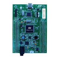
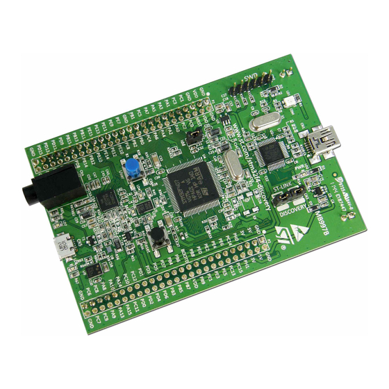
ST STM32F4 Series User Manual (35 pages)
Discovery kit
Brand:
ST
| Category:
Computer Hardware
| Size: 1.2 MB
Table of Contents
Table of Contents
2
Conventions
6
Table 1. ON/OFF Conventions
6
Quick Start
7
Getting Started
7
System Requirements
7
Development Toolchains Supporting the STM32F411 Discovery Kit
7
Order Code
7
Features
8
Hardware Layout
9
Figure 2. Hardware Block Diagram
9
Figure 3. Top Layout
10
Figure 4. Bottom Layout
11
Embedded ST-LINK/V2
12
Table 2. Jumper States
12
Figure 5. Typical Configuration
12
Using ST-LINK/V2 to Program/Debug the STM32F411 on Board
13
Figure 6. STM32F411 Discovery Board Connections Image
13
Using ST-LINK/V2 to Program/Debug an External STM32 Application
14
Table 3. Debug Connector CN2 (SWD)
14
Figure 7. ST-LINK Connections Image
14
Power Supply and Power Selection
15
Leds
15
Pushbuttons
15
On Board Audio Capability
16
USB OTG Supported
16
E-Compass MEMS (ST MEMS LSM303DLHC)
16
Gyroscope MEMS (ST MEMS L3GD20)
16
JP2 (IDD)
17
OSC Clock
17
OSC Clock Supply
17
OSC 32 Khz Clock Supply
17
BOOT0 Configuration
18
Solder Bridges
18
Table 4. Solder Bridges
18
Extension Connectors
19
Table 5. MCU Pin Description Versus Board Function
19
Mechanical Drawing
27
Figure 8. STM32F411 Discovery Board Mechanical Drawing
27
Electrical Schematics
28
Figure 1. STM32F411 Discovery Board
28
Figure 9. STM32F411 Discovery Board
28
Figure 10. ST-LINK/V2 (SWD Only)
29
Figure 11. STM32F411VET6 MCU
30
Figure 12. Audio
31
Figure 13. USB_OTG_FS
32
Figure 14. Peripherals
33
Table 6. Document Revision History
34
ST STM32F4 Series Manual (5 pages)
Brand:
ST
| Category:
Computer Hardware
| Size: 1.71 MB
Table of Contents
Introduction
1
Prerequisites
1
Hardware
1
Software
1
Source Files
1
Demo Bring up
1
Hardware Setup
1
Application Bring up
3
Limitations/Known Issues
4
References
4
Article Sources and Contributors
5
Image Sources, Licenses and Contributors
5
Advertisement
Related Products
ST STM32F469I-DISCO
ST STM32F411
ST STM32F411E-DISCO
ST STM32F47
ST STM32F429NIH6
ST STM32F407IEH7
ST STM32F407ZGT6J
ST STM32F429BGT6
ST STM32F429NIH6J
ST STM32F334C8
ST Categories
Motherboard
Computer Hardware
Microcontrollers
Control Unit
Controller
More ST Manuals
Login
Sign In
OR
Sign in with Facebook
Sign in with Google
Upload manual
Upload from disk
Upload from URL