Xilinx ZCU102 User Manual
Hide thumbs
Also See for ZCU102:
- Tutorial (56 pages) ,
- Software install and board setup (41 pages) ,
- Manual (17 pages)
Table of Contents
Advertisement
Quick Links
Advertisement
Table of Contents

Related Manuals for Xilinx ZCU102


Summary of Contents for Xilinx ZCU102
- Page 1 ZCU102 Evaluation Board User Guide UG1182 (v1.2) March 20, 2017...
-
Page 2: Revision History
2-1) to rev 1.0. Updated Table 2-1 Table 2-3. Updated Chapter 3, Component Descriptions. Updated Appendix B, Master Constraints File Listing. 05/11/2016 Initial Xilinx release - limited distribution. ZCU102 Evaluation Board User Guide www.xilinx.com Send Feedback UG1182 (v1.2) March 20, 2017... -
Page 3: Table Of Contents
UART1 (MIO 20-21) ............... .60 ZCU102 Evaluation Board User Guide www.xilinx.com... - Page 4 ZCU102 Board Constraints File Listing ........
- Page 5 Please Read: Important Legal Notices ..........136 ZCU102 Evaluation Board User Guide www.xilinx.com...
-
Page 6: Chapter 1: Introduction
Chapter 1 Introduction Overview The ZCU102 is a general purpose evaluation board for rapid-prototyping based on the ™ Zynq® UltraScale+ XCZU9EG-2FFVB1156I MPSoC (multiprocessor system-on-chip). High speed DDR4 SODIMM and component memory interfaces, FMC expansion ports, multi-gigabit per second serial transceivers, a variety of peripheral interfaces, and FPGA logic for user customized designs provides a flexible prototyping platform. -
Page 7: Block Diagram
Chapter 1: Introduction Block Diagram The ZCU102 board block diagram is shown in Figure 1-1. Page numbers in the block diagram reference the corresponding page number(s) of schematic 0381701. X-Ref Target - Figure 1-1 Prototype Header PMOD SDIO SYSMON IIC... -
Page 8: Board Features
Chapter 1: Introduction Board Features The ZCU102 evaluation board features are listed here. Detailed information for each feature is provided in Chapter 3, Board Component Descriptions. • XCZU9EG-2FFVB1156I MPSoC • PL V for range in datasheet CCINT • Form factor for PCIe Gen2x4 Host, Micro-ATX chassis footprint •... - Page 9 • Power Management The ZCU102 evaluation board provides designers a rapid prototyping platform utilizing the XCZU9EG-2FFVB1156I device. The ZU9EG contains many useful processor system (PS) hard block peripherals exposed through the Multi-use I/O (MIO) interface and a variety of FPGA programmable logic (PL), high-density (HD) and high-performance (HP) banks.
-
Page 10: Board Specifications
Thickness: 0.104 in. (0.2642 cm) Notes: • A 3D model of this board is not available. • ZCU102 board documentation (xdc listing, schematics, layout files and board outline/fab drawings, etc.) is available on the web at: www.xilinx.com/zcu102. Environmental Temperature Operating: 0°C to +45°C Storage: -25°C to +60°C... -
Page 11: Chapter 2: Board Setup And Configuration
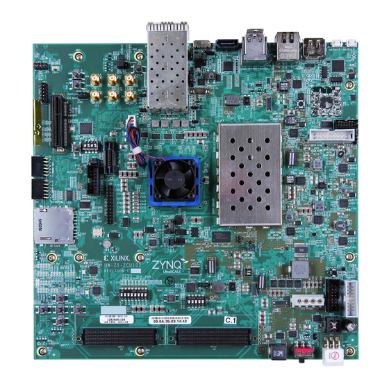
Always refer to the schematic and xdc of the specific ZCU102 version of interest for such details. Electrostatic discharge (ESD) can cause board damage. Follow standard ESD prevention CAUTION! measures when handling the board. - Page 12 Chapter 2: Board Setup and Configuration X-Ref Target - Figure 2-1 Figure 2-1: ZCU102 Evaluation Board Components ZCU102 Evaluation Board User Guide www.xilinx.com Send Feedback UG1182 (v1.2) March 20, 2017...
- Page 13 Chapter 2: Board Setup and Configuration Table 2-1: ZCU102 Board Components Schematic Callout Ref. Des. Feature/Component Notes 0381449 Page Number Zynq UltraScale XCZU9EG MPSoC XCZU9EG-2FFVB1156I with fan sink on soldered FPGA Radian FA35+K52B+T710 PS-Side: DDR4 SODIMM Socket LOTES ADDR0067-P001A with SODIMM...
- Page 14 Chapter 2: Board Setup and Configuration Table 2-1: ZCU102 Board Components (Cont’d) Schematic Callout Ref. Des. Feature/Component Notes 0381449 Page Number SW20 User I/O (CPU_RESET pushbutton switch, active High) E-Switch TL3301EP100QG DIP Switch, 5-pole, GPIO (TI MSP430 System 5 pole C&K SDA05H1SBD...
-
Page 15: Default Switch And Jumper Settings
Table 2-3 (for default jumper settings). Both tables reference the respective schematic page numbers. X-Ref Target - Figure 2-2 Figure 2-2: DIP Switch and Board Header Jumper Locations ZCU102 Evaluation Board User Guide www.xilinx.com Send Feedback UG1182 (v1.2) March 20, 2017... -
Page 16: Switches
SYSMON I2C Address • Open: SYSMON_VN_R floating • 1-2: SYSMON_VP_N pulled down SYSMON VREFP • 1-2: 1.25V VREFP connected to FPGA • 2-3: VREFP connected to GND ZCU102 Evaluation Board User Guide www.xilinx.com Send Feedback UG1182 (v1.2) March 20, 2017... - Page 17 • 2-3: Host Mode USB ULPI ID select J109 • 1-2: Connector ID • 2-3: VDD33 ID USB ULPI Shield GND select J112 • 1-2: Capacitor • 2-3: GND ZCU102 Evaluation Board User Guide www.xilinx.com Send Feedback UG1182 (v1.2) March 20, 2017...
- Page 18 • OFF: rails power on normally • 1-2: all rails (except UTIL) OFF PS_DDR4_VPP_2V5 power inhibit (U39) • OFF: rail powers on normally • 1-2: PS_DDR4_VPP_2V5 OFF J164 MSP430 firmware upgrade header ZCU102 Evaluation Board User Guide www.xilinx.com Send Feedback UG1182 (v1.2) March 20, 2017...
-
Page 19: Mpsoc Device Configuration
Vivado, SDK, or third-party tools can establish a JTAG connection to the Zynq UltraScale+ MPSoC device through one of the three provided JTAG interfaces: 1. Xilinx platform USB or cable PC4 connector (J8) 2. ARM 20-pin JTAG connector (J6) 3. Digilent SMT2.5 USB-to-JTAG module with off-module micro-USB connector (J2) -
Page 20: Chapter 3: Board Component Descriptions
The processing system in a Zynq UltraScale+ MPSoC features the ARM® flagship Cortex®-A53 64-bit quad-core processor and Cortex-R5 dual-core real-time processor. Production ZCU102 Evaluation boards will ship with -2LE speed grade devices. Support of multiple speed grades requires voltage adjustments. The PL-side V... - Page 21 PCIe DDRC (DDR4/3/3L, LPDDR3/4) 128 KB RAM To ACP Gen4 32-bit/64-bit Battery Low Power Full Power Power 64-bit 128-bit Figure 3-1: Zynq UltraScale+ MPSoC Top-Level Block Diagram ZCU102 Evaluation Board User Guide www.xilinx.com Send Feedback UG1182 (v1.2) March 20, 2017...
- Page 22 Architecture and Product Overview (DS890) [Ref 1], and the Zynq UltraScale+ MPSoC Technical Reference Manual (UG1085) [Ref 2] for more information about Zynq UltraScale+ MPSoC configuration options. ZCU102 Evaluation Board User Guide www.xilinx.com Send Feedback UG1182 (v1.2) March 20, 2017...
- Page 23 Chapter 3: Board Component Descriptions Encryption Key Backup Circuit The XCZU9EG MPSoC U1 implements bitstream encryption key technology. The ZCU102 board provides the encryption key backup battery circuit shown in Figure 3-2 X-Ref Target - Figure 3-2 Figure 3-2: Encryption Key Backup Circuit The Seiko TS518FE rechargeable 1.5V lithium button-type battery B1 is soldered to the...
-
Page 24: Ps-Side: Ddr4 Sodimm Socket
2-1, callout 2] The PS-side memory is wired to the Zynq UltraScale+ DDRC hard memory controller. A 64-bit single rank DDR4 SODIMM with ECC (72-bit) is inserted into socket J1. The ZCU102 is shipped with a DDR4 SODIMM installed: •... - Page 25 Chapter 3: Board Component Descriptions The ZCU102 supports full power-off suspend mode where only the system controller and the PS-side DDR4 SODIMM memory are powered. The DDR4 memory is kept in a self-refresh state and has its reset input controlled by the system controller such that the memory is not reset when waking-up from suspend mode.
- Page 26 AJ30 DDR4_SODIMM_DQ36 DQ36 AK29 DDR4_SODIMM_DQ37 DQ37 AK30 DDR4_SODIMM_DQ38 DQ38 AJ29 DDR4_SODIMM_DQ39 DQ39 AE27 DDR4_SODIMM_DQ40 DQ40 AF28 DDR4_SODIMM_DQ41 DQ41 AF30 DDR4_SODIMM_DQ42 DQ42 AF31 DDR4_SODIMM_DQ43 DQ43 AD28 DDR4_SODIMM_DQ44 DQ44 ZCU102 Evaluation Board User Guide www.xilinx.com Send Feedback UG1182 (v1.2) March 20, 2017...
- Page 27 AM34 DDR4_SODIMM_CB6 CB6/NC AL33 DDR4_SODIMM_CB7 CB7/NC AN17 DDR4_SODIMM_DM0_B DM0_N/DBI0_N AM21 DDR4_SODIMM_DM1_B DM1_N/DBI1_N AK19 DDR4_SODIMM_DM2_B DM2_N/DBI2_N AH24 DDR4_SODIMM_DM3_B DM3_N/DBI3_N AH31 DDR4_SODIMM_DM4_B DM4_N/DBI4_N AE30 DDR4_SODIMM_DM5_B DM5_N/DBI5_N AJ31 DDR4_SODIMM_DM6_B DM6_N/DBI6_N ZCU102 Evaluation Board User Guide www.xilinx.com Send Feedback UG1182 (v1.2) March 20, 2017...
- Page 28 AJ27 DDR4_SODIMM_CKE1 CKE1 AM30 DDR4_SODIMM_ODT0 ODT0 AJ26 DDR4_SODIMM_ODT1 ODT1 AM24 DDR4_SODIMM_RAS_B RAS_N/A16 AK24 DDR4_SODIMM_CAS_B CAS_N/A15 AK25 DDR4_SODIMM_WE_B WE_N/A14 AG25 DDR4_SODIMM_ACT_B ACT_N AF22 DDR4_SODIMM_ALERT_B ALERT_N AF20 DDR4_SODIMM_PARITY PARITY ZCU102 Evaluation Board User Guide www.xilinx.com Send Feedback UG1182 (v1.2) March 20, 2017...
-
Page 29: Ddr4 Component Memory
AL30 DDR4_SODIMM_CS1_B CS1_N The ZCU102 DDR4 SODIMM interface adheres to the constraints guidelines documented in the PCB Guidelines for DDR4 section of UltraScale Architecture PCB Design Guide (UG583) [Ref 3] The ZCU102 DDR4 SODIMM interface is a 40Ω impedance implementation. Other... - Page 30 DDR4_DQ11 POD12_DCI DQU3 DDR4_DQ12 POD12_DCI DQU4 DDR4_DQ13 POD12_DCI DQU5 DDR4_DQ14 POD12_DCI DQU6 DDR4_DQ15 POD12_DCI DQU7 DDR4_DQS0_T DIFF_POD12 DQSL_T DDR4_DQS0_C DIFF_POD12 DQSL_C DDR4_DQS1_T DIFF_POD12 DQSU_T DDR4_DQS1_C DIFF_POD12 DQSU_C ZCU102 Evaluation Board User Guide www.xilinx.com Send Feedback UG1182 (v1.2) March 20, 2017...
- Page 31 POD12_DCI DML_B/DBIL_B DDR4_DM1 POD12_DCI DMU_B/DBIU_B The ZCU102 board DDR4 16-bit component memory interface adheres to the constraints Note: guidelines documented in the PCB Guidelines for DDR4 section of UltraScale Architecture PCB Design User Guide (UG583) [Ref 3]. The ZCU102 DDR4 component interface is a 40Ω impedance implementations.
-
Page 32: Psmio
Chapter 3: Board Component Descriptions PSMIO Table 3-5 provides PS MIO peripheral mapping implemented on the ZCU102 board. See the Zynq UltraScale+ MPSoC Technical Reference Manual (UG1085) [Ref 2] for more information on PS MIO peripheral mapping. Table 3-5: ZCU102 MIO Connections... -
Page 33: Quad-Spi Flash Memory (Mio 0-12)
Manual (UG1085) [Ref 2] provides details on using the Quad-SPI flash memory. For more QSPI details, see the Micron MT25QU512ABB8ESF-0SIT data sheet at the Micron website [Ref 13]. ZCU102 Evaluation Board User Guide www.xilinx.com Send Feedback UG1182 (v1.2) March 20, 2017... -
Page 34: Usb 3.0 Transceiver And Usb 2.0 Ulpi Phy
Figure 3-3). A USB cable is supplied in the ZCU102 Evaluation Kit (standard-A connector to host computer, micro-B connector to ZCU102 board connector J96). The USB3320 is a high-speed USB 2.0 PHY supporting the UTMI+ low pin interface (ULPI) interface standard. The ULPI standard defines the interface between the USB controller IP and the PHY device which drives the physical USB bus. - Page 35 J96 pins 2-3 (default). The USB shield can optionally be connected through a capacitor to GND by installing a capacitor (body size 0402) at location C887 and jumping pins 1-2 on header J112. ZCU102 Evaluation Board User Guide www.xilinx.com Send Feedback...
- Page 36 2, which will turn on LED DS51 if overcurrent or thermal shutdown conditions are detected. DS51 is located in the U116 circuit area near push-button SW2 (Figure 2-1, callout X-Ref Target - Figure 3-4 Figure 3-4: ULPI U116 Transceiver Circuit ZCU102 Evaluation Board User Guide www.xilinx.com Send Feedback UG1182 (v1.2) March 20, 2017...
-
Page 37: Sd Card Interface
[Figure 2-1, callout 6] The ZCU102 board includes a secure digital input/output (SDIO) interface to provide access to general purpose non-volatile SDIO memory cards and peripherals. Information for the SD I/O card specification can be found at the SanDisk Corporation... - Page 38 CMD_SD DATA3_SD DATA2_SD ENABLE Figure 3-5 shows the connections of the SD card interface on the ZCU102 board. X-Ref Target - Figure 3-5 Figure 3-5: SD Card Interface Table 3-10 lists the SD card interface connections to the XCZU9EG MPSoC.
- Page 39 U133 IP4856CX25 Adapter XCZU9EG (U1) Net Name Pin Number Pin Name MIO41_SDIO_DIR_DAT0 DIR_0 MIO42_SDIO_DIR_DAT1_3 DIR_1_3 MIO46_SDIO_DAT0 DATA0_H MIO47_SDIO_DAT1 DATA1_H MIO48_SDIO_DAT2 DATA2_H MIO49_SDIO_DAT3 DATA3_H MIO50_SDIO_CMD CMD_H MIO51_SDIO_CLK CLK_IN MIO44_SDIO_PROTECT MIO45_SDIO_DETECT ZCU102 Evaluation Board User Guide www.xilinx.com Send Feedback UG1182 (v1.2) March 20, 2017...
-
Page 40: Programmable Logic Jtag Programming Options
• J8 2x7 2 mm shrouded, keyed JTAG pod flat cable connector • J6 2x10 ARM JTAG male pin header The ZCU102 board JTAG chain is shown in Figure 3-6. X-Ref Target - Figure 3-6 Figure 3-6: JTAG Chain Block Diagram ZCU102 Evaluation Board User Guide www.xilinx.com... -
Page 41: Emio Arm Trace Port
JTAG chain connects to the XCZU9EG MPSoC. EMIO ARM Trace Port [Figure 2-1, callout 43] The ZCU102 evaluation board provides a trace/debug 38-pin Mictor connector, P6. Figure 3-7 shows connector P6 with its MPSoC Bank 47/48 connections. X-Ref Target - Figure 3-7... - Page 42 TRACESRST_B LVCMOS33 For more information about managing the Zynq MPSoC extended MIO (EMIO) trace port connections refer to the Zynq UltraScale+ MPSoC Technical Reference Manual (UG1085) [Ref ZCU102 Evaluation Board User Guide www.xilinx.com Send Feedback UG1182 (v1.2) March 20, 2017...
-
Page 43: Clock Generation
Chapter 3: Board Component Descriptions Clock Generation The ZCU102 board provides fixed and variable clock sources for the XCZU9EG MPSoC. Table 3-12 lists the source devices for each clock. Table 3-12: ZCU102 Board Clock Sources Clock Name Frequency Clock Source... - Page 44 The SI5341B is a one-time programmable clock source. For more details refer to the SI5341B data sheet [Ref 17] for more details. The clock circuit is shown in Figure 3-8. ZCU102 Evaluation Board User Guide www.xilinx.com Send Feedback UG1182 (v1.2) March 20, 2017...
- Page 45 On power-up the user clock defaults to an output frequency of 300.000 MHz. User applications can change the output frequency within the range of 10 MHz to 810 MHz through an I2C interface. Power cycling the ZCU102 board reverts this user clock to the default frequency of 300.000 MHz.
- Page 46 156.250 MHz. User applications can change the output frequency within the range of 10 MHz to 810 MHz through an I2C interface. Power cycling the ZCU102 board reverts this user clock to the default frequency of 156.250 MHz.
- Page 47 [Figure 2-1, callout 42] The ZCU102 board provides a pair of SMAs for differential AC coupled user MGT clock input into FPGA U1 MGTH bank 129. This differential signal pair is series-capacitor coupled. The P-side SMA J79 signal USER_SMA_MGT_CLOCK_P is connected to U1 MGTREFCLK0P pin J27, with the N-side SMA J80 signal USER_SMA_MGT_CLOCK_N connected to U1 MGTREFCLK0N pin J28.
-
Page 48: Gem3 Ethernet (Mio 64-77)
PHY address 5'b01100 (0x0C) and Auto Negotiation set to Enable. Communication with the device is covered in the DP83867 RGMII PHY data sheet [Ref 18]. X-Ref Target - Figure 3-12 Figure 3-12: Ethernet Block Diagram ZCU102 Evaluation Board User Guide www.xilinx.com Send Feedback UG1182 (v1.2) March 20, 2017... -
Page 49: 10/100/1000 Mhz Tri-Speed Ethernet Phy
Board Component Descriptions 10/100/1000 MHz Tri-Speed Ethernet PHY [Figure 2-1, callout 12] The ZCU102 board uses the TIDP83867IRPAP Ethernet RGMII PHY [Ref 18] at U98 for Ethernet communications at 10 Mb/s, 100 Mb/s, or 1000 Mb/s. The board supports RGMII mode only. - Page 50 The LED functions can be re-purposed with a LEDCR1 register write available via the PHY's management Data Interface, MDIO/MDC. LED_2 is assigned to ACT (activity indicator) and ZCU102 Evaluation Board User Guide www.xilinx.com Send Feedback UG1182 (v1.2) March 20, 2017...
-
Page 51: Cp2108 Usb Uart Interface
[Figure 2-1, callout 13] The CP2108 quad USB-UART on the ZCU102 board provides four level-shifted UART connections through single micro-B USB connector J83. Channel 0 and 1 are PS-side MIO connections described in the MIO section. Channel 2 is a PL-side connection and Channel 3 is connected to MSP430 system controller U41. - Page 52 Table 3-16: XCZU9EG U1 to CP2108 U40 Connections via L/S U52 CP2108 U40 XCZU9EG (U1) Schematic Net Name Pin Name Pin No. UART2_TXD_O_FPGA_RXD TX_2 UART2_RXD_I_FPGA_TXD RX_2 UART2_RTS_O_B RTS_2 UART2_CTS_I_B CTS_2 ZCU102 Evaluation Board User Guide www.xilinx.com Send Feedback UG1182 (v1.2) March 20, 2017...
-
Page 53: Gpio (Mio 13, 38)
3-18. Table 3-18: System Controller U41 GPIO Connections to XCZU9EG U1 MSP430 U41 XCZU9EG Net Name (U1) Pin Pin Name Pin No. MIO13_PS_GPIO2 AK17 P1_7 MIO38_PS_GPIO1 P1_6 ZCU102 Evaluation Board User Guide www.xilinx.com Send Feedback UG1182 (v1.2) March 20, 2017... -
Page 54: I2C0 (Mio 14-15)
TCA6416A U97 connections. The devices on each bus of the I2C0 multiplexer U60 are identified in Table 3-21 and the multiplexer bus connections are listed in Table 3-22. ZCU102 Evaluation Board User Guide www.xilinx.com Send Feedback UG1182 (v1.2) March 20, 2017... - Page 55 VCCPSDDRPLL_EN MI026_PMU_INPUT_LS PL_PMBUS_ALERT PS_PMBUS_ALERT MAXIM_PMBUS_ALERT PL_DDR4_VTERM_EN PL_DDR4_VPP_2V5_EN PS_DIMM_VDDQ_TO_PSVCCO_ON PS_DIMM_SUSPEND_EN PS_DDR4_VTERM_EN PS_DDR4_VPP_2V5_EN PS_GTR_LANE_SEL0 PS_GTR_LANE_SEL1 PS_GTR_LANE_SEL2 PS_GTR_LANE_SEL3 PCIE_CLK_DIR_SEL IIC_MUX_RESET_B GEM3_EXP_RESET_B FMC_HPC0_PRSNT_M2C_B FMC_HPC1_PRSNT_M2C_B MAXIM_PMBUS_SDA/SCL SYSMON_SDA/SCL Figure 3-17: I2C0 Bus Topology ZCU102 Evaluation Board User Guide www.xilinx.com Send Feedback UG1182 (v1.2) March 20, 2017...
- Page 56 Refer to connections shown in Figure 3-17. (TCA6416A U97 Addr. 0x20) I2C0_SCL PS_GTR_LANE_SEL0 U125 PI2DBS6212 PS_GTR_LANE_SEL1 U126 PI2DBS6212 PS_GTR_LANE_SEL2 U127 PI2DBS6212 PS_GTR_LANE_SEL3 U128 PI2DBS6212 PCIE_CLK_DIR_SEL U139 SN74AVC1T45 ZCU102 Evaluation Board User Guide www.xilinx.com Send Feedback UG1182 (v1.2) March 20, 2017...
- Page 57 INA226 MGTRAVTT 0X45 INA226 VCCO_PSDDR_504 0X46 INA226 VCCOPS 0X47 INA226 VCCOPS3 0X4A INA226 VCCPSDDRPLL 0X4B PL_PMBUS INA226 VCCINT 0X40 INA226 VCCBRAM 0X41 INA226 VCCAUX 0X42 INA226 VCC1V2 0X43 ZCU102 Evaluation Board User Guide www.xilinx.com Send Feedback UG1182 (v1.2) March 20, 2017...
-
Page 58: I2C1 (Mio 16-17)
I2C1 bus connectivity represented in Table 3-23 Table 3-24. TCA9548A U34 is set to 0x74 and TCA9548A U135 is set to 0x75. ZCU102 Evaluation Board User Guide www.xilinx.com Send Feedback UG1182 (v1.2) March 20, 2017... - Page 59 U34 I2C Mux I2C BUS 1 Device(s) (Addr 0x74) Port EEPROM Si5341 Clock USER Si570 clock USER MGT Si570 clock Si5328 (Clock recovery) No connection No connection No connection ZCU102 Evaluation Board User Guide www.xilinx.com Send Feedback UG1182 (v1.2) March 20, 2017...
-
Page 60: Uart0 (Mio 18-19)
CP2108 Channel 1 PS-side UART interface circuit is shown in Figure 3-19. The connections from XCZU9EG U1 to CP2108 U40 via L/S U54 are listed in Table 3-26. ZCU102 Evaluation Board User Guide www.xilinx.com Send Feedback UG1182 (v1.2) March 20, 2017... -
Page 61: Gpio (Mio 22-23)
The PS-side CAN bus TX and RX MIO pins go through TXS0104E level-translator U33 and TI SN65HVD232 CAN-bus transceiver U122 before being presented to the user on 0.1 inch centered 8-pin male header J98 (see Figure 3-20 Figure 3-21). ZCU102 Evaluation Board User Guide www.xilinx.com Send Feedback UG1182 (v1.2) March 20, 2017... -
Page 62: Pmu Gpi (Mio 26)
DisplayPort standard defines an auxiliary channel that uses LVDS signaling at a 1 Mb/s data rate, which is translated from single-ended MIO signals to the differential DisplayPort AUX channel, DPAUX (see Table 3-27). The DisplayPort circuit is shown in Figure 3-22. ZCU102 Evaluation Board User Guide www.xilinx.com Send Feedback UG1182 (v1.2) March 20, 2017... - Page 63 Table 3-27: DPAUX/MIO Connections Level Shifter U114 XCZU9EG Schematic Net Name (U1) Pin Pin Name Pin No. MIO30_DP_AUX_IN MIO29_DP_OE MIO28_DP_HPD MIO27_DP_AUX_OUT X-Ref Target - Figure 3-22 Figure 3-22: DisplayPort Circuit ZCU102 Evaluation Board User Guide www.xilinx.com Send Feedback UG1182 (v1.2) March 20, 2017...
-
Page 64: Pcie Reset (Mio 31)
[Figure 2-1, callout 14] The ZCU102 board provides a high-definition multimedia interface (HDMI®) video output using a TI SN65DP159RGZ HDMI re-timer at U94. The HDMI output is provided on a TE Connectivity 1888811-1 right-angle dual-stacked HDMI type-A receptacle at P7. The SN65DP159RGZ device is a dual mode DisplayPort to transition-minimized differential signal (TMDS) re-timer supporting digital video interface (DVI) 1.0 and high-definition... - Page 65 Figure 3-24. The connections between the codec and the XCZU9EG MPSoC are listed in Table 3-29. X-Ref Target - Figure 3-23 Figure 3-23: HDMI Interface Block Diagram ZCU102 Evaluation Board User Guide www.xilinx.com Send Feedback UG1182 (v1.2) March 20, 2017...
- Page 66 IN_D1N HDMI_TX2_P IN_D2P SN65DP159 HDMI_TX2_N IN_D2N (U94) HDMI_TX_LVDS_OUT_P IN_CLKP LVDS HDMI_TX_LVDS_OUT_N LVDS IN_CLKN HDMI_TX_SRC_SCL LVCMOS33 SCL_SRC HDMI_TX_SRC_SDA LVCMOS33 SDA_SRC HDMI_TX_EN LVCMOS33 HDMI_CTL_SCL LVCMOS33 SCL_CTL HDMI_CTL_SDA LVCMOS33 SDA_CTL ZCU102 Evaluation Board User Guide www.xilinx.com Send Feedback UG1182 (v1.2) March 20, 2017...
-
Page 67: Hdmi Clock Recovery
[Figure 2-1, callout 40] The ZCU102 board includes a Silicon Labs Si5324C jitter attenuator U70 (2 kHz - 945 MHz). The FPGA can output the RX recovered clock to a differential I/O pair on I/O bank 66 (HDMI_REC_CLOCK_C_P, pin Y8 and HDMI_REC_CLOCK_C_N, pin Y7) for jitter attenuation. -
Page 68: Sfp/Sfp+ Connector
Figure 3-25: HDMI Interface Clock Recovery SFP/SFP+ Connector [Figure 2-1, callout 17] The ZCU102 board contains a small form-factor pluggable (SFP+) 2x2 quad-connector and cage assembly that accepts SFP or SFP+ modules. Figure 3-26 shows a typical SFP+ module connector circuitry implementation. - Page 69 RL13 RL_RD_P SFP1_RX_N RL12 RL_RD_N SFP1_TX_DISABLE RL_ TX_DISABLE Location Left Top SFP2 SFP2_TX_P LT_TD_P LT18 SFP2_TX_N LT19 LT_TD_N SFP2_RX_P LT13 LT_RD_P SFP2_RX_N LT_RD_N LT12 SFP2_TX_DISABLE LT_ TX_DISABLE ZCU102 Evaluation Board User Guide www.xilinx.com Send Feedback UG1182 (v1.2) March 20, 2017...
-
Page 70: Sfp/Sfp+ Clock Recovery
[Figure 2-1, callout 11] The ZCU102 board includes a Silicon Labs Si5328B jitter attenuator U20 (8 kHz - 808 MHz). The FPGA can output the RX recovered clock to a differential I/O pair on I/O bank 67 (SFP_REC_CLOCK_C_P, pin R10 and SFP_REC_CLOCK_C_N, pin R9) for jitter attenuation. -
Page 71: User Pmod Gpio Headers
User PMOD GPIO Headers [Figure 2-1, callout 19] The ZCU102 evaluation board supports two PMOD GPIO headers J55 (right-angle female) and J87 (vertical male). The PMOD nets are wired to the XCZU9EG device U1 bank 47. Figure 3-28 shows the GPIO PMOD headers J55 and J87. -
Page 72: Prototype Header
[Ref 23]. Prototype Header [Figure 2-1, callout 41] The ZCU102 evaluation board provides a 2x12 male header prototype header J3 which makes ten Bank 50 GPIO connections available. Figure 3-29 shows connector J3 with its MPSoC (U1) Bank 50 connections. - Page 73 I/O Standard (U1) Pin Header J3 Pin L12N_AD8N_50_N LVCMOS33 L12N_AD8P_50_P LVCMOS33 L11N_AD9N_50_N LVCMOS33 L11N_AD9P_50_P LVCMOS33 L10N_AD10N_50_N LVCMOS33 L10N_AD10P_50_P LVCMOS33 L9N_AD11N_50_N LVCMOS33 L9N_AD11P_50_P LVCMOS33 L8N_HDGC_50_P LVCMOS33 L8N_HDGC_50_N LVCMOS33 ZCU102 Evaluation Board User Guide www.xilinx.com Send Feedback UG1182 (v1.2) March 20, 2017...
-
Page 74: User I2C0 Receptacle
Board Component Descriptions User I2C0 Receptacle [Figure 2-1, callout 20] The ZCU102 evaluation board supports a PMOD 2X6 receptacle (right-angle female) J160. Figure 3-30 shows the I2C0 PMOD receptacle J160. The I2C0 nets are a branch of the I2C0 main bus (see... - Page 75 Table 3-33 lists the GPIO to XCZU9EG U1 connections. X-Ref Target - Figure 3-31 Figure 3-31: GPIO LEDs X-Ref Target - Figure 3-32 Figure 3-32: GPIO Pushbutton Switches ZCU102 Evaluation Board User Guide www.xilinx.com Send Feedback UG1182 (v1.2) March 20, 2017...
- Page 76 SW14.3 GPIO_SW_S AE15 LVCMOS33 SW16.3 AG13 GPIO_SW_C LVCMOS33 SW15.3 CPU Reset Pushbutton (Active High) AM13 CPU_RESET LVCMOS33 SW20.3 GPIO DIP SW (Active High) AN14 GPIO_DIP_SW0 LVCMOS33 SW13.8 ZCU102 Evaluation Board User Guide www.xilinx.com Send Feedback UG1182 (v1.2) March 20, 2017...
-
Page 77: Power And Status Leds
VCCPSPLL 1.2VDC Power ON DS15 Green DS16 VCCPSINTLP_PGOOD Green VCCPSINTLP 0.85VDC Power ON DS17 DDR4_DIMM_VDDQ_PGOOD Green DDR4_DIMM_VDDQ 1.2VDC Power ON MGTRAVTT_PGOOD MGTRAVTT 1.81VDC Power ON DS18 Green ZCU102 Evaluation Board User Guide www.xilinx.com Send Feedback UG1182 (v1.2) March 20, 2017... - Page 78 PS USB 3.0 ULPI VBUS Power Error Notes: 1. See the Zynq UltraScale+ MPSoC Technical Reference Manual (UG1085) [Ref 2] for more information about Zynq UltraScale+MPSoC configuration pins. ZCU102 Evaluation Board User Guide www.xilinx.com Send Feedback UG1182 (v1.2) March 20, 2017...
-
Page 79: Gth Transceivers
The GTH transceivers in the XCZU9EG device are grouped into four channels referred to as Quads. The reference clock for a Quad can be sourced from the Quad above or Quad below the GTH Quad of interest. There are six GTH Quads on the ZCU102 board with connectivity as shown here: •... - Page 80 Quad 230: • MGTREFCLK0 - USER_MGT_SI570_CLOCK2_C_P/N • MGTREFCLK1 - SFP_SI5328_OUT_C_P/N • Contains 4 GTH transceivers allocated to SFP[0:3]_TX/RX_P/N GTH usage on the ZCU102 is shown in Figure 3-35. ZCU102 Evaluation Board User Guide www.xilinx.com Send Feedback UG1182 (v1.2) March 20, 2017...
- Page 81 Available MGT reference clocks include the FMC defined GBT clocks 0 and 1 for HPC_1, a programmable Si570 clock, and a user provided SMA clock. The MGT reference clocks are located in adjacent MGT banks, 128, 129, and 130. ZCU102 Evaluation Board User Guide www.xilinx.com Send Feedback...
- Page 82 One (1) MGT in Bank 128 is provided on a SMA connector pair. Available MGT clocks include a user provided MGT reference clock on an SMA connector pair, and a programmable Si570 clock. Table 3-35 lists GTH bank 128 connections. ZCU102 Evaluation Board User Guide www.xilinx.com Send Feedback UG1182 (v1.2) March 20, 2017...
- Page 83 Chapter 3: Board Component Descriptions Table 3-35: ZCU102 GTH Bank 128 Interface Connections Connected To XCZU9EG XCZU9EG (U1) Pin Schematic Net Name (U1) Pin Name Pin No. Pin Name Device MGTHTXP0_128 HDMI_TX0_P IN_D0P MGTHTXN0_128 HDMI_TX0_N IN_D0N TI SN65DP159RGZ MGTHTXP1_128 HDMI_TX1_P...
- Page 84 Chapter 3: Board Component Descriptions Table 3-36 lists GTH bank 129 connections. Table 3-36: ZCU102 GTH Bank 129 Interface Connections Connected To XCZU9EG XCZU9EG (U1) Pin Schematic Net Name (U1) Pin Name Pin No. Pin Name Device MGTHTXP0_129 FMC_HPC1_DP4_C2M_P DP4_C2M_P...
- Page 85 Chapter 3: Board Component Descriptions Table 3-37 lists GTH bank 130 connections. Table 3-37: ZCU102 GTH Bank 130 Interface Connections Connected To XCZU9EG XCZU9EG (U1) Pin Schematic Net Name (U1) Pin Name Pin No. Pin Name Device MGTHTXP0_130 FMC_HPC1_DP0_C2M_P DP0_C2M_P...
- Page 86 Chapter 3: Board Component Descriptions Table 3-38 lists GTH bank 228 connections. Table 3-38: ZCU102 GTH Bank 228 Interface Connections Connected To XCZU9EG XCZU9EG (U1) Pin Schematic Net Name (U1) Pin Name Pin No. Pin Name Device MGTHTXP0_228 FMC_HPC0_DP6_C2M_P DP6_C2M_P...
- Page 87 Chapter 3: Board Component Descriptions Table 3-39 lists GTH bank 229 connections. Table 3-39: ZCU102 GTH Bank 229 Interface Connections Connected To XCZU9EG XCZU9EG (U1) Pin Schematic Net Name (U1) Pin Name Pin No. Pin Name Device MGTHTXP0_229 FMC_HPC0_DP3_C2M_P DP3_C2M_P...
- Page 88 Chapter 3: Board Component Descriptions Table 3-40 lists GTH bank 230 connections. Table 3-40: ZCU102 GTH Bank 230 Interface Connections Connected To XCZU9EG XCZU9EG (U1) Pin Schematic Net Name (U1) Pin Name Pin No. Pin Name Device MGTHTXP0_230 SFP0_TX_P RT_TD_P...
-
Page 89: Ps-Side: Gtr Transceivers
Zynq UltraScale+ MPSoC Technical Reference Manual (UG1085) [Ref Table 3-41 lists the interconnect matrix (ICM). Table 3-42 lists the interconnect matrix settings and GTR lane functionality. ZCU102 Evaluation Board User Guide www.xilinx.com Send Feedback UG1182 (v1.2) March 20, 2017... - Page 90 The GTR selections provided with GT switch topology shown in Figure 3-37 are: 1. PCIe Gen2/1 x4 2. DisplayPort (2-Lanes), USB, SATA 3. PCIe Gen2/1 x2, USB, SATA 4. PCIe Gen2/1 x1, DisplayPort (1-Lane), USB, SATA ZCU102 Evaluation Board User Guide www.xilinx.com Send Feedback UG1182 (v1.2) March 20, 2017...
- Page 91 S = 0 connects the A input to the B output, whereas S = 1, connects the A input to the C output. The "S" select logic is implemented with GPIO pins to support the settings listed Table 3-43. ZCU102 Evaluation Board User Guide www.xilinx.com Send Feedback UG1182 (v1.2) March 20, 2017...
-
Page 92: Pcie (Mio 31)
USB, SATA PCIe (MIO 31) The ZCU102 hosts a 4-lane PCIe root port connector similar to those commonly used on many micro-ATX motherboards. The PS-side GTR transceivers can be set to provide a PCI Express interface that operates at GEN2 speeds with a width of 1-lane (x1), 2-lanes (x2), or 4-lanes (x4). -
Page 93: Fpga Mezzanine Card Interface
FPGA Mezzanine Card Interface [Figure 2-1, callouts 31, 32] The ZCU102 evaluation board supports the VITA 57.1 FPGA mezzanine card (FMC) specification [Ref 22] by providing subset implementations of high pin count connectors at J5 (HPC0) and J4 (HPC1). HPC connectors use a 10 x 40 form factor, populated with 400 pins. - Page 94 Chapter 3: Board Component Descriptions The ZCU102 board FMC VADJ voltage VADJ_FMC_BUS for the J5 (HPC0) and J4 (HPC1) FMC connectors is determined by the MAX15301 U63 voltage regulator described in ZCU102 Board Power System, page 110. The valid values of the VADJ_FMC rail are 1.2V, 1.5V, and 1.8V.
- Page 95 4. J5 HPC0 TDO-TDI connections to U27 HPC0 FMC JTAG bypass switch (N.C. normally-closed/bypassing J5 until an FMC card is plugged onto J5). 5. Sourced from VADJ_FMC_BUS voltage regulator U63 MAX15301 pin 32 power good output signal. ZCU102 Evaluation Board User Guide www.xilinx.com Send Feedback...
- Page 96 Table 3-46: J5 HPC0 FMC Section E and F Connections to XCZU9EG U1 J5 Pin Schematic Net Name U1 Pin J5 Pin Schematic Net Name U1 Pin Standard Standard FMC_HPC0_PG_M2C P/U to 3.3V via R277 VADJ_FMC_BUS VADJ_FMC_BUS ZCU102 Evaluation Board User Guide www.xilinx.com Send Feedback UG1182 (v1.2) March 20, 2017...
- Page 97 VADJ_FMC_BUS FMC_HPC0_LA32_P LVCMOS18 FMC_HPC0_LA32_N LVCMOS18 VADJ_FMC_BUS Notes: 1. FMC_HPC0_PRSNT_M2C_B is the HPC FMC JTAG bypass switch U27.4 OE control signal is driven from I2C I/O expander U97.13. ZCU102 Evaluation Board User Guide www.xilinx.com Send Feedback UG1182 (v1.2) March 20, 2017...
-
Page 98: Fmc Hpc1 Connector J4
The FMC connector at J4 (HPC1) implements a subset of the full FMC HPC connectivity: • 60 single-ended, or 30 differential user-defined pairs (LA[00:29]) • Eight GTH transceiver DP differential pairs • Two GBTCLK differential clocks ZCU102 Evaluation Board User Guide www.xilinx.com Send Feedback UG1182 (v1.2) March 20, 2017... - Page 99 Board Component Descriptions • 159 ground and 15 power connections The ZCU102 board FMC VADJ voltage VADJ_FMC_BUS for the J5 (HPC0) and J4 (HPC1) FMC connectors is determined by the MAX15301 U63 voltage regulator described in ZCU102 Board Power System, page 110.
- Page 100 4. J5 HPC0 TDO-TDI connections to U27 HPC0 FMC JTAG bypass switch (N.C. normally-closed/bypassing J5 until an FMC card is plugged onto J5). 5. Sourced from VADJ_FMC_BUS voltage regulator U63 MAX15301 pin 32 power good output signal. ZCU102 Evaluation Board User Guide www.xilinx.com Send Feedback...
- Page 101 Table 3-51: J4 HPC1 FMC Section E and F Connections to XCZU9EG U1 J5 Pin Schematic Net Name U1 Pin J5 Pin Schematic Net Name U1 Pin Standard Standard FMC_HPC0_PG_M2C P/U to 3.3V via R250 VADJ_FMC_BUS VADJ_FMC_BUS ZCU102 Evaluation Board User Guide www.xilinx.com Send Feedback UG1182 (v1.2) March 20, 2017...
- Page 102 FMC_HPC1_LA33_N FMC_HPC1_LA30_N VADJ_FMC_BUS FMC_HPC1_LA32_P FMC_HPC1_LA32_N VADJ_FMC_BUS Notes: 1. FMC_HPC0_PRSNT_M2C_B is the HPC FMC JTAG bypass switch U27.4 OE control signal is driven from I2C I/O expander U97.13. ZCU102 Evaluation Board User Guide www.xilinx.com Send Feedback UG1182 (v1.2) March 20, 2017...
- Page 103 J5 Pin Schematic Net Name U1 Pin Standard Standard See the ANSI/VITA 57.1 FPGA mezzanine card (FMC) specification [Ref 22] for additional information on the FPGA FMC. ZCU102 Evaluation Board User Guide www.xilinx.com Send Feedback UG1182 (v1.2) March 20, 2017...
-
Page 104: Cooling Fan Connector
V is set to ADJ_FMC the lowest value compatible with the ZCU102 board and the FMC modules, within the available choices of 1.8V, 1.5V, 1.2V, and 0.0V. • If no valid information is found in an FMC card IIC EEPROM, the V... -
Page 105: Ti Msp430 System Controller
This GUI enables you to query and control select programmable features such as clocks, FMC functionality, power systems, and the Zynq UltraScale+ MPSoC GTR selection compatible with your design. The ZCU102 web page also includes a tutorial on the SCUI (XTP433) - Page 106 The MSP430 firmware might be updated in the event new capability is added in the future. Note: The MSP430 upgrade header, J164, is reserved for this purpose. Xilinx will provide information on the update procedure via future updates to XTP433 [Ref 11].
-
Page 107: Switches
Do NOT plug a PC ATX power supply 6-pin connector into J52 on the ZCU102 board. The CAUTION! ATX 6-pin connector has a different pin-out than J52. Connecting an ATX 6-pin connector into J52 damages the ZCU102 board and voids the board warranty. - Page 108 PS software can then act on. See the Zynq UltraScale+ MPSoC Technical Reference Manual (UG1085) [Ref 2] for information about Zynq UltraScale+ MPSoC configuration. X-Ref Target - Figure 3-42 Figure 3-42: PS_PROG_B Pushbutton Switch SW5 ZCU102 Evaluation Board User Guide www.xilinx.com Send Feedback UG1182 (v1.2) March 20, 2017...
- Page 109 EN_ are High, all OUT_ are high, and MR is de-asserted. See the Zynq UltraScale+ MPSoC Technical Reference Manual (UG1085) [Ref 2] for information for information concerning the resets. ZCU102 Evaluation Board User Guide www.xilinx.com Send Feedback UG1182 (v1.2) March 20, 2017...
-
Page 110: Zcu102 Board Power System
Board Component Descriptions ZCU102 Board Power System [Figure 2-1, callout 34] The ZCU102 hosts a Maxim PMBus based power system. Each individual Maxim MAX20751EKX, MAX15301, or MAX15303 voltage regulator has a PMBus interface. Figure 3-44 shows the ZCU102 power system block diagram. - Page 111 Chapter 3: Board Component Descriptions The ZCU102 evaluation board uses power regulators and PMBus compliant POL controllers from Maxim Integrated Circuits [Ref 21] to supply the core and auxiliary voltages listed in Table 3-55. The schematic page references are to 0381701.
-
Page 112: Monitoring Voltage And Current
Chapter 3: Board Component Descriptions Table 3-55: ZCU102 Power System Devices (Cont’d) Ref. PMBus Power Rail Net Power Rail INA226 Schematic Device Type Description Des. Address Name Voltage Address Page MAX8869E U143 Maxim LDO Regulator 1A UTIL_1V13 1.13V MAX8869E Maxim LDO Regulator 1A UTIL_1V8 1.80V... - Page 113 Chapter 3: Board Component Descriptions Table 3-56: ZCU102 Power Rails with INA226 Power Monitors PMBus Power Rail Net INA226 Schematic Device Type Ref. Des. Address Name Address Page MAX15301 VCCINT PL: 0x40 0x13 MAX15303 VCCBRAM PL: 0x41 0x14 MAX15303 VCCAUX...
-
Page 114: Appendix A: Vita 57.1 Fmc Connector Pinouts
Figure A-1 shows the pinout of the FPGA mezzanine card (FMC) high pin count (HPC) connector defined by the VITA 57.1 FMC specification. For a description of how the ZCU102 evaluation board implements the FMC specification, see FPGA Mezzanine Card Interface,... -
Page 115: Appendix B: Master Constraints File Listing
Master Constraints File Listing Overview The master Xilinx design constraints (XDC) file template for the ZCU102 board provides for designs targeting the ZCU102 evaluation board. Net names in the constraints listed correlate with net names on the latest ZCU102 evaluation board schematic. Identify the appropriate pins and replace the net names with net names in the user RTL. - Page 116 #GTR 505 FIXED CLOCKS SOURCED FROM U69 SI5341B #Other net PACKAGE_PIN AA27 - GTR_REF_CLK_PCIE_C_P #Other net PACKAGE_PIN AA28 - GTR_REF_CLK_PCIE_C_N #Other net PACKAGE_PIN W27 - GTR_REF_CLK_SATA_C_P #Other net PACKAGE_PIN W28 - GTR_REF_CLK_SATA_C_N ZCU102 Evaluation Board User Guide www.xilinx.com Send Feedback UG1182 (v1.2) March 20, 2017...
- Page 117 PACKAGE_PIN AP24 - DDR4_SODIMM_DQ10 Bank 504 - PS_DDR_DQ10 #Other net PACKAGE_PIN AN23 - DDR4_SODIMM_DQ11 Bank 504 - PS_DDR_DQ11 #Other net PACKAGE_PIN AL21 - DDR4_SODIMM_DQ12 Bank 504 - PS_DDR_DQ12 ZCU102 Evaluation Board User Guide www.xilinx.com Send Feedback UG1182 (v1.2) March 20, 2017...
- Page 118 PACKAGE_PIN AM33 - DDR4_SODIMM_CB5 Bank 504 - PS_DDR_DQ69 #Other net PACKAGE_PIN AM34 - DDR4_SODIMM_CB6 Bank 504 - PS_DDR_DQ70 #Other net PACKAGE_PIN AL33 - DDR4_SODIMM_CB7 Bank 504 - PS_DDR_DQ71 ZCU102 Evaluation Board User Guide www.xilinx.com Send Feedback UG1182 (v1.2) March 20, 2017...
- Page 119 [get_ports "DDR4_A15_CAS_B"] set_property PACKAGE_PIN AJ9 [get_ports "DDR4_A16_RAS_B"] set_property IOSTANDARD SSTL12_DCI [get_ports "DDR4_A16_RAS_B"] set_property PACKAGE_PIN AK12 [get_ports "DDR4_BA0"] set_property IOSTANDARD SSTL12_DCI [get_ports "DDR4_BA0"] set_property PACKAGE_PIN AJ12 [get_ports "DDR4_BA1"] ZCU102 Evaluation Board User Guide www.xilinx.com Send Feedback UG1182 (v1.2) March 20, 2017...
- Page 120 [get_ports "DDR4_PAR"] set_property IOSTANDARD SSTL12_DCI [get_ports "DDR4_PAR"] set_property PACKAGE_PIN AK8 [get_ports "DDR4_ACT_B"] set_property IOSTANDARD SSTL12_DCI [get_ports "DDR4_ACT_B"] set_property PACKAGE_PIN AK9 [get_ports "DDR4_ODT"] set_property IOSTANDARD SSTL12_DCI [get_ports "DDR4_ODT"] ZCU102 Evaluation Board User Guide www.xilinx.com Send Feedback UG1182 (v1.2) March 20, 2017...
- Page 121 [get_ports "FMC_HPC0_DP4_M2C_P"] set_property PACKAGE_PIN P5 [get_ports "FMC_HPC0_DP5_C2M_N"] set_property PACKAGE_PIN P6 [get_ports "FMC_HPC0_DP5_C2M_P"] set_property PACKAGE_PIN P1 [get_ports "FMC_HPC0_DP5_M2C_N"] set_property PACKAGE_PIN P2 [get_ports "FMC_HPC0_DP5_M2C_P"] set_property PACKAGE_PIN R3 [get_ports "FMC_HPC0_DP6_C2M_N"] ZCU102 Evaluation Board User Guide www.xilinx.com Send Feedback UG1182 (v1.2) March 20, 2017...
- Page 122 [get_ports "FMC_HPC0_LA11_P"] set_property IOSTANDARD LVCMOS18 [get_ports "FMC_HPC0_LA11_P"] set_property PACKAGE_PIN W6 [get_ports "FMC_HPC0_LA12_N"] set_property IOSTANDARD LVCMOS18 [get_ports "FMC_HPC0_LA12_N"] set_property PACKAGE_PIN W7 [get_ports "FMC_HPC0_LA12_P"] set_property IOSTANDARD LVCMOS18 [get_ports "FMC_HPC0_LA12_P"] ZCU102 Evaluation Board User Guide www.xilinx.com Send Feedback UG1182 (v1.2) March 20, 2017...
- Page 123 [get_ports "FMC_HPC0_LA26_N"] set_property PACKAGE_PIN L15 [get_ports "FMC_HPC0_LA26_P"] set_property IOSTANDARD LVCMOS18 [get_ports "FMC_HPC0_LA26_P"] set_property PACKAGE_PIN L10 [get_ports "FMC_HPC0_LA27_N"] set_property IOSTANDARD LVCMOS18 [get_ports "FMC_HPC0_LA27_N"] set_property PACKAGE_PIN M10 [get_ports "FMC_HPC0_LA27_P"] ZCU102 Evaluation Board User Guide www.xilinx.com Send Feedback UG1182 (v1.2) March 20, 2017...
- Page 124 [get_ports "FMC_HPC1_DP3_M2C_N"] set_property PACKAGE_PIN B33 [get_ports "FMC_HPC1_DP3_M2C_P"] set_property PACKAGE_PIN K30 [get_ports "FMC_HPC1_DP4_C2M_N"] set_property PACKAGE_PIN K29 [get_ports "FMC_HPC1_DP4_C2M_P"] set_property PACKAGE_PIN L32 [get_ports "FMC_HPC1_DP4_M2C_N"] set_property PACKAGE_PIN L31 [get_ports "FMC_HPC1_DP4_M2C_P"] ZCU102 Evaluation Board User Guide www.xilinx.com Send Feedback UG1182 (v1.2) March 20, 2017...
- Page 125 [get_ports "FMC_HPC1_LA10_N"] set_property PACKAGE_PIN AH4 [get_ports "FMC_HPC1_LA10_P"] set_property IOSTANDARD LVCMOS18 [get_ports "FMC_HPC1_LA10_P"] set_property PACKAGE_PIN AF8 [get_ports "FMC_HPC1_LA11_N"] set_property IOSTANDARD LVCMOS18 [get_ports "FMC_HPC1_LA11_N"] set_property PACKAGE_PIN AE8 [get_ports "FMC_HPC1_LA11_P"] ZCU102 Evaluation Board User Guide www.xilinx.com Send Feedback UG1182 (v1.2) March 20, 2017...
- Page 126 [get_ports "FMC_HPC1_LA25_N"] set_property IOSTANDARD LVCMOS18 [get_ports "FMC_HPC1_LA25_N"] set_property PACKAGE_PIN AE10 [get_ports "FMC_HPC1_LA25_P"] set_property IOSTANDARD LVCMOS18 [get_ports "FMC_HPC1_LA25_P"] set_property PACKAGE_PIN R12 [get_ports "FMC_HPC1_LA26_N"] set_property IOSTANDARD LVCMOS18 [get_ports "FMC_HPC1_LA26_N"] ZCU102 Evaluation Board User Guide www.xilinx.com Send Feedback UG1182 (v1.2) March 20, 2017...
- Page 127 [get_ports "HDMI_TX_CEC"] set_property PACKAGE_PIN B16 [get_ports "HDMI_TX_HPD"] set_property IOSTANDARD LVCMOS33 [get_ports "HDMI_TX_HPD"] set_property PACKAGE_PIN C16 [get_ports "HDMI_TX_SRC_SCL"] set_property IOSTANDARD LVCMOS33 [get_ports "HDMI_TX_SRC_SCL"] set_property PACKAGE_PIN D16 [get_ports "HDMI_TX_SRC_SDA"] ZCU102 Evaluation Board User Guide www.xilinx.com Send Feedback UG1182 (v1.2) March 20, 2017...
- Page 128 [get_ports "TRACEDATA6"] set_property IOSTANDARD LVCMOS33 [get_ports "TRACEDATA6"] set_property PACKAGE_PIN J17 [get_ports "TRACEDATA5"] set_property IOSTANDARD LVCMOS33 [get_ports "TRACEDATA5"] set_property PACKAGE_PIN H19 [get_ports "TRACEDATA4"] set_property IOSTANDARD LVCMOS33 [get_ports "TRACEDATA4"] ZCU102 Evaluation Board User Guide www.xilinx.com Send Feedback UG1182 (v1.2) March 20, 2017...
- Page 129 [get_ports "GPIO_LED_3"] set_property IOSTANDARD LVCMOS33 [get_ports "GPIO_LED_3"] set_property PACKAGE_PIN AJ15 [get_ports "GPIO_LED_4"] set_property IOSTANDARD LVCMOS33 [get_ports "GPIO_LED_4"] set_property PACKAGE_PIN AH13 [get_ports "GPIO_LED_5"] set_property IOSTANDARD LVCMOS33 [get_ports "GPIO_LED_5"] ZCU102 Evaluation Board User Guide www.xilinx.com Send Feedback UG1182 (v1.2) March 20, 2017...
- Page 130 [get_ports "L10N_AD10N_50_N"] set_property PACKAGE_PIN J14 [get_ports "L10P_AD10P_50_P"] set_property IOSTANDARD LVCMOS33 [get_ports "L10P_AD10P_50_P"] set_property PACKAGE_PIN G14 [get_ports "L9N_AD11N_50_N"] set_property IOSTANDARD LVCMOS33 [get_ports "L9N_AD11N_50_N"] set_property PACKAGE_PIN G15 [get_ports "L9P_AD11P_50_P"] ZCU102 Evaluation Board User Guide www.xilinx.com Send Feedback UG1182 (v1.2) March 20, 2017...
- Page 131 PACKAGE_PIN C13[get_ports "SFP3_TX_DISABLE"] set_property IOSTANDARDLVCMOS33 [get_ports "SFP3_TX_DISABLE"] #SFP COMMON set_property PACKAGE_PIN R9[get_ports "SFP_REC_CLOCK_C_N"] set_property IOSTANDARDLVDS[get_ports "SFP_REC_CLOCK_C_N"] set_property PACKAGE_PIN R10[get_ports "SFP_REC_CLOCK_C_P"] set_property IOSTANDARDLVDS[get_ports "SFP_REC_CLOCK_C_P"] set_property PACKAGE_PIN B9[get_ports "SFP_SI5328_OUT_C_N"] ZCU102 Evaluation Board User Guide www.xilinx.com Send Feedback UG1182 (v1.2) March 20, 2017...
- Page 132 [get_ports "UART2_RXD_I_FPGA_TXD"] set_property IOSTANDARD LVCMOS33 [get_ports "UART2_RXD_I_FPGA_TXD"] set_property PACKAGE_PIN D12 [get_ports "UART2_RTS_O_B"] set_property IOSTANDARD LVCMOS33 [get_ports "UART2_RTS_O_B"] set_property PACKAGE_PIN E12 [get_ports "UART2_CTS_I_B"] set_property IOSTANDARD LVCMOS33 [get_ports "UART2_CTS_I_B"] ZCU102 Evaluation Board User Guide www.xilinx.com Send Feedback UG1182 (v1.2) March 20, 2017...
-
Page 133: Appendix C: Regulatory And Compliance Information
Overview This product is designed and tested to conform to the European Union directives and standards described in this section. Refer to the ZCU102 board master answer record concerning the CE requirements for the PC Test Environment: www.xilinx.com/support/answers/66752 Declaration of Conformity Zynq UltraScale+ ZCU102 Declaration of Conformity is online. -
Page 134: Electromagnetic Compatibility
This product complies with Directive 2002/95/EC on the restriction of hazardous substances (RoHS) in electrical and electronic equipment. This product complies with CE Directives 2006/95/EC, Low Voltage Directive (LVD) and 2004/108/EC, Electromagnetic Compatibility (EMC) Directive. ZCU102 Evaluation Board User Guide www.xilinx.com Send Feedback UG1182 (v1.2) March 20, 2017... -
Page 135: Appendix D: Additional Resources And Legal Notices
Topics include design assistance, advisories, and troubleshooting tips. References The most up to date information related to the ZCU102 board and its documentation is available on the following websites. ZCU102 Evaluation Kit ZCU102 Evaluation Kit —... -
Page 136: Please Read: Important Legal Notices
(including loss of data, profits, goodwill, or any type of loss or damage suffered as a result of any action brought by a third party) even if such damage or loss was reasonably foreseeable or Xilinx had been advised of the possibility of the same. - Page 137 Additional Resources and Legal Notices warranty and support terms contained in a license issued to you by Xilinx. Xilinx products are not designed or intended to be fail-safe or for use in any application requiring fail-safe performance; you assume sole risk and liability for use of Xilinx products in such critical applications, please refer to Xilinx’s Terms of Sale which can be viewed at http://www.xilinx.com/legal.htm#tos.
Need help?
Do you have a question about the ZCU102 and is the answer not in the manual?
Questions and answers