Table of Contents
Advertisement
Quick Links
Advertisement
Table of Contents

Related Manuals for Xilinx ZCU111


Summary of Contents for Xilinx ZCU111
- Page 1 ZCU111 Evaluation Board User Guide UG1271 (v1.1) August 6, 2018...
-
Page 2: Revision History
Table 3-18 Table 3-19 Added optional RFMC and SYSREF capacitor options. Added note and reference to SNIA Technology SFP28 Module Connectors Affiliates website. 06/28/2018 Version 1.0 Initial Xilinx release. ZCU111 Board User Guide Send Feedback UG1271 (v1.1) August 6, 2018 www.xilinx.com... -
Page 3: Table Of Contents
CAN1 (MIO 24-25) ............... . .35 ZCU111 Board User Guide Send Feedback UG1271 (v1.1) August 6, 2018... - Page 4 ZCU111 System Controller ........
- Page 5 Xilinx Resources ........
-
Page 6: Chapter 1: Introduction
(SDFEC), and FPGA fabric and RFSoC features, such as the quad core Arm® Cortex™-A53 processing system (PS) and the dual-core Arm Cortex-R5 real-time processors. The ZCU111 evaluation board is equipped with many of the common board-level features needed for design development, such as DDR4 memory, networking interfaces, FMC+ expansion port, and access to the new RF-FMC interface. -
Page 7: Block Diagram
RFMC_ADC[04:05] RFMC_ADC[02:03] RFMC_ADC[00:01] X21110-062118 Figure 1-1: ZCU111 Evaluation Board Block Diagram Board Features The ZCU111 evaluation board features are listed here. Detailed information for each feature is provided in Board Component Descriptions in Chapter • XCZU28DR-2E, FFVG1517 package • Form factor: rectangular 11.811 in. x 7.874 in. x 0.1 in. - Page 8 PS MIO[18:19]: UART (one of three FT4232 UART channels) ° PS MIO[22:23]: PS_PB, PS_LED I/F ° PS MIO[26]: platform management unit (PMU) ° PS MIO[27:30]: DisplayPort control ° ZCU111 Board User Guide Send Feedback UG1271 (v1.1) August 6, 2018 www.xilinx.com...
-
Page 9: Board Specifications
Operational status LEDs (INIT, DONE, PS STATUS, PGOOD) • Power management • System controller (MSP430) The ZCU111 provides a rapid prototyping platform using the XCZU28DR-2EFFVG1517 device. See the Zynq UltraScale+ RFSoC Data Sheet: Overview (DS889) [Ref 1] for a feature set overview, description, and ordering information. -
Page 10: Environmental
Chapter 1: Introduction Environmental Temperature Operating: 0°C to +45°C Storage: -25°C to +60°C Humidity 10% to 90% non-condensing Operating Voltage +12 V ZCU111 Board User Guide Send Feedback UG1271 (v1.1) August 6, 2018 www.xilinx.com... -
Page 11: Chapter 2: Board Setup And Configuration
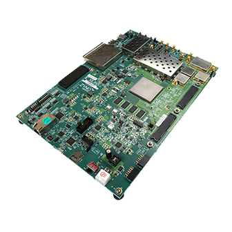
Always refer to the schematic, layout, and XDC files of the specific ZCU111 version of interest for such details. The ZCU111 board can be damaged by electrostatic discharge (ESD). Follow standard ESD CAUTION! prevention measures when handling the board. - Page 12 Round callout references a component Square callout references a component on the front side of the board on the back side of the board X20477-06211 Figure 2-1: ZCU111 Evaluation Board Components ZCU111 Board User Guide Send Feedback UG1271 (v1.1) August 6, 2018 www.xilinx.com...
- Page 13 I/O, user 8-pole DIP switch, SW14 C&K SDA08H1SBD active High User I/O, CPU_RESET pushbutton, SW20 E-switch TL3301EP100QG active High System controller 5-pole C&K SDA05H1SBD Switches, PS_SRST_B, PS_POR_B SW3, SW4 E-switch TL3301EP100QG pushbuttons ZCU111 Board User Guide Send Feedback UG1271 (v1.1) August 6, 2018 www.xilinx.com...
- Page 14 RF clocking, U90 LMK04208 RF J108 Rosenberger 32K10K-400L5 REFCLK SMA RF clocking, U90 LMK04208 RF J109 Rosenberger 32K10K-400L5 external REFCLK SMA RF clocking, LMK04208 RF REFCLK TI LMK04208 ZCU111 Board User Guide Send Feedback UG1271 (v1.1) August 6, 2018 www.xilinx.com...
- Page 15 TI SN74AVC8T245PWR Power and Status LEDs, LED driver TI SN74AVC8T245PWR Power and Status LEDs, LED driver TI SN74AVC8T245PWR PB U42 MSP430 reset, E-switch TL3301EP100QG PB reset (U42 MSP430). ZCU111 Board User Guide Send Feedback UG1271 (v1.1) August 6, 2018 www.xilinx.com...
-
Page 16: Default Jumper And Switch Settings
Chapter 2: Board Setup and Configuration Default Jumper and Switch Settings Figure 2-2 shows the ZCU111 board jumper header and switch locations. Each numbered component shown in the figure is keyed to Table 2-2 (for default jumper settings) or Table 2-3 (for default switch settings). -
Page 17: Jumpers
1-2: track SD3.0 J100 socket UTIL_3V3 3.3V 2-3: GND = revert to internal voltage reference U93 SC18IS602IPW I2C-to-SPI bridge enable On: U93 bridge RESET_B to GND, U93 inhibited ZCU111 Board User Guide Send Feedback UG1271 (v1.1) August 6, 2018 www.xilinx.com... - Page 18 On: bank 228 DAC_REXT pin W8 = GND Off: bank 228 DAC_REXT pin W8 = 2.49K to GND J101 SPI CS select header 1-2: 3-4: 5-6: 7-8: J111 SPI SDO select header 1-2: 3-4: 5-6: ZCU111 Board User Guide Send Feedback UG1271 (v1.1) August 6, 2018 www.xilinx.com...
-
Page 19: Switches
Switch Off = 0 = Low; On = 1 = High SW15 CPU_RESET pushbutton SW16 Main power slide switch SW19 PS MIO22_BUTTON pushbutton Notes: 1. Pushbutton switch default = open (not pressed). ZCU111 Board User Guide Send Feedback UG1271 (v1.1) August 6, 2018 www.xilinx.com... -
Page 20: Rfsoc Device Configuration
1110 Notes: 1. Default switch setting. JTAG Vivado®, Xilinx SDK, or third-party tools can establish a JTAG connection to the Zynq UltraScale+ RFSoC device through the FTDI FT4232 USB-to-JTAG/USB UART device (U34) connected to micro-USB connector (J83). Quad SPI To boot from the dual Quad SPI nonvolatile configuration memory: 1. - Page 21 Chapter 2: Board Setup and Configuration See the Zynq UltraScale+ Device Technical Reference Manual (UG1085) [Ref 3] for more information about Zynq UltraScale+ RFSoC configuration options. ZCU111 Board User Guide Send Feedback UG1271 (v1.1) August 6, 2018 www.xilinx.com...
-
Page 22: Chapter 3: Board Component Descriptions
Component Descriptions Zynq UltraScale+ XCZU28DR RFSoC [Figure 2-1, callout 1] The ZCU111 board is populated with the Zynq UltraScale+ XCZU28DR-2FFVG1517 RFSoC, which combines a powerful processing system (PS) and programmable logic (PL) in the ® ® same device. The PS in a Zynq UltraScale+ RFSoC features the Arm... -
Page 23: Encryption Key Battery Backup Circuit
Chapter 3: Board Component Descriptions Encryption Key Battery Backup Circuit The XCZU28DR RFSoC U1 implements bitstream encryption key technology. The ZCU111 board provides the encryption key backup battery circuit shown in Figure 3-1. X-Ref Target - Figure 3-1 X20480-062118 Figure 3-1: Encryption Key Backup Circuit The Seiko TS518FE rechargeable 1.5V lithium button-type battery B1 is soldered to the... -
Page 24: Ps-Side: Ddr4 Sodimm Socket
VCC1V2 1.2V PS_DDR4 64-BIT SODIMM I/F Notes: 1. The ZCU111 board is shipped with VADJ_FMC set to 1.8V by the MSP430 system controller. PS-Side: DDR4 SODIMM Socket [Figure 2-1, callout 2] The PS-side memory is wired to the Zynq UltraScale+ DDRC bank 504 hard memory controller. -
Page 25: Pl-Side: Ddr4 Component Memory
Chapter 3: Board Component Descriptions The ZCU111 XCZU28DR RFSoC PS DDR interface maximum 2133 MT/s performance is documented in the Zynq UltraScale+ RFSoC Data Sheet (DS926)[Ref The ZCU111 DDR4 SODIMM interface adheres to the constraints guidelines documented in the PCB guidelines for DDR4 section of the UltraScale Architecture PCB Design User Guide... -
Page 26: Psmio
Chapter 3: Board Component Descriptions PSMIO Table 3-2 provides PS MIO peripheral mapping implemented on the ZCU111 board. See the Zynq UltraScale+ Device Technical Reference Manual (UG1085) [Ref 3] for more information on PS MIO peripheral mapping. Table 3-2: MIO Peripheral Mapping... -
Page 27: Quad Spi Flash Memory (Mio 0-12)
U42 system controller and the XCZU28DR RFSoC are listed in Table 3-3. Table 3-3: System Controller U42 GPIO Connections to XCZU28DR U1 MSP430 U42 XCZU28DR (U1) Net Name Pin Name Pin # MIO38_PS_GPIO1 P1_6 MIO13_PS_GPIO2 P1_7 ZCU111 Board User Guide Send Feedback UG1271 (v1.1) August 6, 2018 www.xilinx.com... -
Page 28: I2C0 (Mio 14-15), I2C1 (Mio 16-17)
U27 TCA9548A I2C1 PMBus Cable 0x75 INA226 PMBus N.C. IRPS5401 PS + PL Voltage Controller PMBus SYSMON I2C0 U23 PCA9544A X20530-062118 Figure 3-2: I2C0 and I2C1 Bus Connectivity Overview ZCU111 Board User Guide Send Feedback UG1271 (v1.1) August 6, 2018 www.xilinx.com... -
Page 29: I2C0 (Mio 14-15)
BANK 64 0x20 PL I2C0 AW16/AT16 TCA6416A INA226_PMBUS_SCA/SCL SD0/SC0 Not Connected SD1/SC1 SDA/ IRPS5401_PMBUS_SDA/SCL SD2/SC2 MPS430 SYSMON_SCA/SCL SD3/SC3 0x75 22 P3_0 23 P3_1 X20531-062118 Figure 3-3: I2C0 Bus Topology ZCU111 Board User Guide Send Feedback UG1271 (v1.1) August 6, 2018 www.xilinx.com... - Page 30 J26(H) ASP_184329_01 PRSNT_M2C_L J26(Z) ASP_184329_01 CLK_SPI_MUX_SEL0 IDTQS3VH253QG8 CLK_SPI_MUX_SEL1 IDTQS3VH253QG8 INT2_B PCA9544A IRPS5401_ALERT_B ALERT_B U53,U55,U57 IRPS5401 SALERT_B U68,U70,U74,U75 IR38060 INT0_B PCA9544A U3,U59-U61 ALERT INA226_PMBUS_ALERT U63-U66 INA226 U67,U69,U71,U73, ALERT U77,U79 ZCU111 Board User Guide Send Feedback UG1271 (v1.1) August 6, 2018 www.xilinx.com...
-
Page 31: I2C1 (Mio 16-17)
I2C address 0x74. TCA9548A U27 is pin-strapped to respond to I2C address 0x75. Figure 3-4 shows a high-level view of the I2C1 bus connectivity represented in Table 3-6 Table 3-7. ZCU111 Board User Guide Send Feedback UG1271 (v1.1) August 6, 2018 www.xilinx.com... - Page 32 NOT CONNECTED SD1/SC1 SYSMON_SDA/SCL SD2/SC2 PS_DDR4_SODIMM_SDA/SCL SDA/SCL SD3/SC3 MPS430 SFP3_IIC_SDA/SCL SD4/SC5 SFP2_IiC_SDA/SCL SD5/SC5 SFP1_IiC_SDA/SCL SD6/SC6 28 P4_1 SFP0_IIC_SDA/SCL 29 P4_2 SD7/SC7 0x75 X20532-062118 Figure 3-4: I2C1 Bus Topology ZCU111 Board User Guide Send Feedback UG1271 (v1.1) August 6, 2018 www.xilinx.com...
- Page 33 0x51 SFP3 P2 0x50 SFP2 P1 0x50 SFP1 P2 0x50 SFP0 P1 0x50 For more information on the TCA9548A and PCA9544A, see the Texas Instruments website [Ref 20]. ZCU111 Board User Guide Send Feedback UG1271 (v1.1) August 6, 2018 www.xilinx.com...
-
Page 34: Uart0 (Mio 18-19)
PS_UART0 (MIO 18-19) Port C UART2 PL_UART2 bank 64 Port D UART3 U42 system controller UART X-Ref Target - Figure 3-5 X20481-062118 Figure 3-5: ZCU111 FT4232HL UART Connections ZCU111 Board User Guide Send Feedback UG1271 (v1.1) August 6, 2018 www.xilinx.com... -
Page 35: Uart1 (Mio 20-21)
The Zynq UltraScale+ RFSoC provides a VESA DisplayPort 1.2 source-only controller that supports up to two lanes of main link data at rates of 1.62 Gb/s, 2.70 Gb/s, or 5.40 Gb/s. The ZCU111 Board User Guide Send Feedback UG1271 (v1.1) August 6, 2018... - Page 36 Table 3-10: DPAUX/MIO Connections SN74AVC4T245 Level Shifter U10 XCZU28DR (U1) Pin Net Name Pin Name Pin # MIO30_DP_AUX_IN MIO29_DP_OE MIO28_DP_HPD MIO27_DP_AUX_OUT X-Ref Target - Figure 3-6 X20482-062118 Figure 3-6: DisplayPort Circuit ZCU111 Board User Guide Send Feedback UG1271 (v1.1) August 6, 2018 www.xilinx.com...
-
Page 37: Pmu Gpo (Mio 32-37)
[Figure 2-1, callout 6] The ZCU111 board includes a secure digital input/output (SDIO) interface to provide access to general purpose non-volatile SDIO memory cards and devices. Information for the SD I/O card specification can be found at the SanDisk Corporation... - Page 38 Chapter 3: Board Component Descriptions Figure 3-7 shows the connections of the SD card interface on the ZCU111 board. X-Ref Target - Figure 3-7 X20483-062118 Figure 3-7: SD Card Interface The NXP SD3.0 level shifter is mounted on an Aries adapter board that has the pin mapping...
-
Page 39: Usb 3.0 Transceiver And Usb 2.0 Ulpi Phy
USB cable is supplied in the ZCU111 evaluation kit (standard-A connector to host computer, USB 3.0 A connector to ZCU111 board connector J96). The USB3320 is a high-speed USB 2.0 PHY supporting the UTMI+ low pin interface (ULPI) interface standard. The ULPI standard defines the interface between the USB controller IP and the PHY device, which drives the physical USB bus. - Page 40 2, which turns on LED DS7 if over current or thermal shutdown conditions are detected. DS7 is located in the U13 circuit area (Figure 2-1, callout 53). Figure 3-9 shows the ULPI U12 transceiver circuit. ZCU111 Board User Guide Send Feedback UG1271 (v1.1) August 6, 2018 www.xilinx.com...
-
Page 41: Gem3 Ethernet (Mio 64-77)
DP83867 RGMII PHY data sheet [Ref 20]. X-Ref Target - Figure 3-10 RGMII RJ45 and Magnetics DP83867IR MDIO X20534-062118 Figure 3-10: Ethernet Block Diagram ZCU111 Board User Guide Send Feedback UG1271 (v1.1) August 6, 2018 www.xilinx.com... -
Page 42: 10/100/1000 Mhz Tri-Speed Ethernet Phy
Chapter 3: Board Component Descriptions 10/100/1000 MHz Tri-Speed Ethernet PHY [Figure 2-1, callout 12] The ZCU111 board uses the TI DP83867IRPAP Ethernet RGMII PHY [Ref 20] (U37) for Ethernet communications at 10 Mb/s, 100 Mb/s, or 1000 Mb/s. The board supports RGMII mode only. - Page 43 Additional functionality is configurable using LEDCR1[7:4] register bits. By default, this pin indicates that link is established. LED_0 S, I/O, PD Additional functionality is configurable using LEDCR1[3:0] register bits. ZCU111 Board User Guide Send Feedback UG1271 (v1.1) August 6, 2018 www.xilinx.com...
-
Page 44: Programmable Logic Jtag Programming Options
• J83 USB micro AB connector connected to U34 FT4232HL USB-JTAG bridge • J13 2x7 2 mm shrouded, keyed JTAG pod flat cable connector The ZCU111 board JTAG chain is shown in Figure 3-12. X-Ref Target - Figure 3-12 JTAG... -
Page 45: Clock Generation
JTAG chain connects to the U1 XCZU28DR RFSoC. Clock Generation The ZCU111 board provides fixed and variable clock sources for the XCZU28DR RFSoC. Table 3-16 lists the source devices for each clock. - Page 46 SFP_REC_CLOCK_N LVDS AW13 Notes: 1. U1 XCZU28DR bank 503 supports LVCMOS18 level inputs. 2. Series capacitor coupled, U1 MGT (I/O standards do not apply). 3. Series capacitor coupled. ZCU111 Board User Guide Send Feedback UG1271 (v1.1) August 6, 2018 www.xilinx.com...
- Page 47 Differential and single-ended outputs The SI5341B is a one-time programmable clock source. The clock circuit is shown in Figure 3-13. X-Ref Target - Figure 3-13 X20486-062118 Figure 3-13: SI5341B Clock Generator ZCU111 Board User Guide Send Feedback UG1271 (v1.1) August 6, 2018 www.xilinx.com...
- Page 48 At power-up, the user clock defaults to an output frequency of 300.000 MHz. User applications can change the output frequency within the range of 10 MHz to 810 MHz through the I2C1 bus interface. Power cycling the ZCU111 board reverts this user clock to the default frequency of 300.000 MHz.
- Page 49 156.250 MHz. User applications can change the output frequency within the range of 10 MHz to 810 MHz through an I2C interface. Power cycling the ZCU111 board reverts this user clock to the default frequency of 156.250 MHz.
- Page 50 [Figure 2-1, callout 48] The ZCU111 board provides a pair of SMAs for differential AC coupled user MGT clock input into FPGA U1 GTY bank 130. This differential signal pair is series-capacitor coupled. The P-side SMA J14 signal USER_SMA_MGT_CLOCK_P is connected to U1 MGTREFCLK1P pin T31, and the N-side SMA J15 signal USER_SMA_MGT_CLOCK_N is connected to U1 MGTREFCLK1N pin T32.
- Page 51 [Figure 2-1, callout 8] The ZCU111 board includes a Silicon Labs SI5382A jitter attenuator U48. The RFSoC U1 PL user logic can implement a clock recovery circuit and output this series capacitor coupled clock from a differential pair on I/O bank 64 (SFP_REC_CLOCK_P U1 pin AW14 and SFP_REC_CLOCK_N U1 pin AW13) for jitter attenuation.
- Page 52 For more details on the Silicon Labs SI5341B, SI570, and SI5382A devices, see [Ref 14]. For UltraScale FPGA clocking information, see the UltraScale Architecture Clocking Resources User Guide (UG572) [Ref 10]. ZCU111 Board User Guide Send Feedback UG1271 (v1.1) August 6, 2018 www.xilinx.com...
-
Page 53: Rf Data Converters
(RF-ADC) channels across four banks and eight multi-gigasample (6.544 GSPS), 14-bit RF digital-to-analog (RF-DAC) converter channels across two banks. The ZCU111 board provides a pair of Samtec LPAF connectors (J47: ADC; J94: DAC) for the RF-ADC/RF-DAC clock and RF signals. - Page 54 Chapter 3: Board Component Descriptions Figure 3-18 shows the bank view of the ZCU111 RF clocking structure. X-Ref Target - Figure 3-18 VCXO Optional DAC: 122.88 MHz SYSREF_RFSOC Loop Capacitor Filter FPGA SMA: AMS_FPGA_REF_CLK Option Bank CPout1 OSCin CLKout0 MPSoC PL: SYSREF_FPGA...
- Page 55 U90 OUT1 N CLK_4208_OUT1_N SYSREF_RFSOC_C_N C743 C1034 Before making ZCU111 RF clock capacitor modifications, refer to the PC board layout and identify the metal RF cage associated with the capacitors of interest: • C632/C640, C646/C718: RFCAGE2 • C683/C690, C692/C699: REFCAGE3 •...
- Page 56 I2C to SPI Bridge LMX2594 Inhibit Jumper RF1 PLL LE_2594_A Muxout LMX2594 RF3 PLL LE_2594_C Muxout LMX2594 RF2 PLL LE_2594_B Muxout X20539-062118 Figure 3-19: I2C_to_SPI Bridge Connectivity for PLL Readback ZCU111 Board User Guide Send Feedback UG1271 (v1.1) August 6, 2018 www.xilinx.com...
-
Page 57: Rf Rfmc Plug-In Card Interface
–TR = tape and reel packaging X-Ref Target - Figure 3-20 X20540-062118 Figure 3-20: SAMTEC Connector The RFMC LPAF connector pin definitions are shown in Figure 3-21 (RF-ADC) and Figure 3-22 (RF-DAC). ZCU111 Board User Guide Send Feedback UG1271 (v1.1) August 6, 2018 www.xilinx.com... - Page 58 Chapter 3: Board Component Descriptions X-Ref Target - Figure 3-21 X20542-062118 Figure 3-21: RFMC RF-ADC LPAF Connector, Vertical Orientation (A1 in Upper Right Corner) ZCU111 Board User Guide Send Feedback UG1271 (v1.1) August 6, 2018 www.xilinx.com...
- Page 59 Chapter 3: Board Component Descriptions X-Ref Target - Figure 3-22 X20543-062118 Figure 3-22: RFMC DAC LPAF Connector, Vertical Orientation (A1 Upper Right Corner) ZCU111 Board User Guide Send Feedback UG1271 (v1.1) August 6, 2018 www.xilinx.com...
-
Page 60: Sfp28 Module Connectors
SFP28 Module Connectors [Figure 2-1, callouts 14, 15] The ZCU111 board hosts four SFP28 connectors J27, J32, J37, and J42. The connectors are housed within a single quad SFP28 cage assembly. The ganged SFP28 cage supports up to four SFP/SFP+/SFP28 modules. - Page 61 Low = Normal operation (1)(2) SFP2 J37 High = Fault SFP_TX_FAULT Test point J38 Low = Normal operation Off = SFP disabled SFP_TX_DISABLE Jumper J40 On = SFP enabled ZCU111 Board User Guide Send Feedback UG1271 (v1.1) August 6, 2018 www.xilinx.com...
- Page 62 2. BW selection is also available via I2C control. For this and additional information about the SFP28 module, see SFF-8402 and SFF-8432 at the specification website [Ref 28]. ZCU111 Board User Guide Send Feedback UG1271 (v1.1) August 6, 2018 www.xilinx.com...
- Page 63 1. Bank 128 GTY connections, I/O standards not applicable. For additional information about the small form factor pluggable SFP28 module, see the SFF-8402 and SFF-8432 specifications at the SNIA Technology Affiliates website [Ref 28]. ZCU111 Board User Guide Send Feedback UG1271 (v1.1) August 6, 2018 www.xilinx.com...
-
Page 64: User Pmod Gpio Connectors
User PMOD GPIO Connectors [Figure 2-1, callout 20, 21] The ZCU111 evaluation board supports two right-angle PMOD GPIO receptacles J48 and J49. The 3.3V PMOD nets are level-shifted and are wired to the XCZU28DR device U1 banks 28, 66, and 68. -
Page 65: User I/O
For more information on the PMOD interface, see the Digilent website [Ref 27]. User I/O [Figure 2-1, callouts 22-25] The ZCU111 board provides these user and general purpose I/O capabilities: • Eight user LEDs (callout 22) GPIO_LED[7-0]: DS11, DS12, DS13, DS14, DS15, DS16, DS17, DS18 ° •... - Page 66 GPIO connections to XCZU28DR U1 connections. X-Ref Target - Figure 3-25 X20493-062118 Figure 3-25: GPIO LEDs X-Ref Target - Figure 3-26 X20494-062118 Figure 3-26: GPIO 8-Pole DIP Switch ZCU111 Board User Guide Send Feedback UG1271 (v1.1) August 6, 2018 www.xilinx.com...
- Page 67 GPIO_LED_3 LVCMOS18 DS14.2 AP15 GPIO_LED_4 LVCMOS18 DS15.2 AN16 GPIO_LED_5 LVCMOS18 DS16.2 AN17 GPIO_LED_6 LVCMOS18 DS17.2 AV15 GPIO_LED_7 LVCMOS18 DS18.2 GPIO DIP SW (Active High) AF16 GPIO_DIP_SW0 LVCMOS18 SW14.8 ZCU111 Board User Guide Send Feedback UG1271 (v1.1) August 6, 2018 www.xilinx.com...
- Page 68 LVCMOS18 SW11.3 GPIO_SW_E LVCMOS18 SW12.3 GPIO_SW_S LVCMOS18 SW13.3 CPU Reset Pushbutton (Active High) AF15 CPU_RESET LVCMOS18 SW15.3 Notes: 1. Level-shifted net names at ZU28DR U1 have _LS appended. ZCU111 Board User Guide Send Feedback UG1271 (v1.1) August 6, 2018 www.xilinx.com...
-
Page 69: Power And Status Leds
DS20 VCCINT_PG Green VCCINT 0.85VDC power on DS21 VCCPSINTFP_PG Green VCCPSINTFP 0.85VDC power on DS22 VCC1V8 Green VCC1V8 1.8VDC power on DS23 VCC1V2_PG Green VCC1V2 1.2VDC power on ZCU111 Board User Guide Send Feedback UG1271 (v1.1) August 6, 2018 www.xilinx.com... - Page 70 LMX2594 U104 lock detect DS45 STATUS_4208 Green LMK04208 status DS49 DAC_AVTT_PG Green DAC_AVTT 2.5VDC power on RF_CLK_VCC3V3_PG Green RF_CLK_VCC3V3 3.3VDC power on DS50 MIO23_LED Green RFSoC U1 bank 500 GPIO LED ZCU111 Board User Guide Send Feedback UG1271 (v1.1) August 6, 2018 www.xilinx.com...
-
Page 71: Gty Transceivers
The GTY transceivers in the XCZU28DR are grouped into four channels or quads. The reference clock for a quad can be sourced from the quad above or the quad below the GTY quad of interest. The four GTY quads used on the ZCU111 board have the connectivity listed in this section. - Page 72 Twelve MGTs are provided by PL-side MGT banks 129, 130, and 131. Available MGT reference clocks include the FMC defined GBT clocks 0, 1 and 2, a programmable SI570 clock and an SMA clock. ZCU111 Board User Guide Send Feedback UG1271 (v1.1) August 6, 2018...
-
Page 73: Ps-Side: Gtr Transceivers
GTY reference clocks include a jitter attenuated recovered clock from a Si5382. SFP+ modules typically provide an I2C based control interface. This I2C interface is accessible for each individual SFP28 module through the I2C multiplexer topology on the ZCU111 board. The RFSoC U1 connections for each quad are referenced in Appendix B, Xilinx Design Constraints. - Page 74 Bank 505 reference clocks are connected to the U46 SI5341B clock generator as detailed in SI5341B 10 Independent Output Any-Frequency Clock Generator, page Bank 505 connections are referenced in Appendix B, Xilinx Design Constraints. ZCU111 Board User Guide Send Feedback UG1271 (v1.1) August 6, 2018 www.xilinx.com...
-
Page 75: Ps M.2 Sata Connector
TX and SATA-B for RX. The M.2 connector U40 is a type 2242 (active component section 22 mm wide with overall length 42 mm form factor) used on socket 2. X-Ref Target - Figure 3-31 X20566-062118 Figure 3-31: M.2 Connector U170 ZCU111 Board User Guide Send Feedback UG1271 (v1.1) August 6, 2018 www.xilinx.com... - Page 76 ADD_IN CARD KEY M ADD_IN CARD KEY M Reserved for MGFG_CLOCK Reserved for MGFG_DATA ALERT# (O) (0/1.8V) SMB_DATA (I/O) (0/1.8V) SMB_CLK (I/O) (0/1.8V) DEVSLP (I) 3.3V 3.3V 3.3V 3.3V DAS/DSS (I/O) ZCU111 Board User Guide Send Feedback UG1271 (v1.1) August 6, 2018 www.xilinx.com...
- Page 77 Table 3-26: M.2 Connector U40 Pinout (Cont’d) Signal 3.3V 3.3V PEDET (GND-SATA) ADD_IN CARD KEY M ADD_IN CARD KEY M ADD_IN CARD KEY M ADD_IN CARD KEY M SATA-A+ SATA-A- SATA-B+ SATA-B- ZCU111 Board User Guide Send Feedback UG1271 (v1.1) August 6, 2018 www.xilinx.com...
- Page 78 Chapter 3: Board Component Descriptions Table 3-26: M.2 Connector U40 Pinout (Cont’d) Signal The M.2 adapter tie-offs as implemented on the ZCU111 board are listed in Table 3-27. Table 3-27: M.2 U40 Connector Tie-offs M.2 Signal Name ZCU111 Tie-Off U40 Pin...
-
Page 79: Fpga Mezzanine Card Interface
FMCP) specification by providing a subset implementation of the high pin count connector at J26 (HSPC). FMC+ connectors use a 14 x 40 form factor, populated with 560 pins. The connector is keyed so that a mezzanine card, when installed on the ZCU111 evaluation board, faces away from the board J26 FMC+ Connector Type •... -
Page 80: Cooling Fan Connector
Figure 3-32. The ZCU111 uses the Infineon MAX6643 (U52) fan controller, which autonomously controls the fan speed by controlling the pulse width modulation (PWM) signal to the fan based on the die temperature sensed via the FPGA's DXP and DXN pins. The fan rotates slowly (acoustically quiet) when the RFSoC is cool and rotates faster as the FPGA heats up (acoustically noisy). -
Page 81: Zcu111 System Controller
Chapter 3: Board Component Descriptions • When an FMC card is attached, its IIC EEPROM is read to find a VADJ voltage supported by both the ZCU111 board and the FMC module, within the available choices of 1.8V, 1.5V, 1.2V, and 0.0V •... - Page 82 Chapter 3: Board Component Descriptions X-Ref Target - Figure 3-33 X20571-062118 Figure 3-33: System Controller User Interface ZCU111 Board User Guide Send Feedback UG1271 (v1.1) August 6, 2018 www.xilinx.com...
-
Page 83: Switches
[Figure 2-1, callout 29] The ZCU111 board power switch is SW1. Sliding the switch actuator from the off to on position applies 12V power from J52, a 6-pin mini-fit connector. Green LED DS19 illuminates when the ZCU111 board power is on. See... - Page 84 PS software. See the Zynq UltraScale+ Device Technical Reference Manual (UG1085) [Ref 3] for information about Zynq UltraScale+ RFSoC configuration. X-Ref Target - Figure 3-35 X20573-062118 Figure 3-35: PS_PROG_B Pushbutton Switch ZCU111 Board User Guide Send Feedback UG1271 (v1.1) August 6, 2018 www.xilinx.com...
- Page 85 It must be held Low through PS power-up. PS_POR_B should be generated by the power supply power-good signal. When the voltage at IN1 is below its threshold or EN1 (P.B. switch SW4 is pressed) goes Low, OUT1 (PS_POR_B) goes Low. ZCU111 Board User Guide Send Feedback UG1271 (v1.1) August 6, 2018...
-
Page 86: Board Power System
Board Power System [Figure 2-15, callout 35] The ZCU111 evaluation board uses power management ICs (PMIC) and power regulators from Infineon [Ref 25] to supply the core and auxiliary voltages listed in Table 3-29. See schematic 0381811. - Page 87 Infineon power controllers is available at the Infineon website [Ref 25]. The PCB layout and power system design meets the recommended criteria described in the UltraScale Architecture PCB Design User Guide (UG583) [Ref ZCU111 Board User Guide Send Feedback UG1271 (v1.1) August 6, 2018 www.xilinx.com...
-
Page 88: Monitoring Voltage And Current
Infineon PMBus controllers and INA226 power monitor op amps. Also, see schematic 0381881. Power rail measurements are accessible to the system controller and RFSoC PL logic through their respective I2C0 bus connections. ZCU111 Board User Guide Send Feedback UG1271 (v1.1) August 6, 2018... -
Page 89: Appendix A: Vita 57.4 Fmcp Connector Pinouts
FPGA plus mezzanine card (FMCP) high pin count (HSPC) connector defined by the VITA 57.4 FMC specification. For a description of how the ZCU111 evaluation board implements the FMCP specification, see FPGA Mezzanine Card Interface, page... -
Page 90: Appendix B: Xilinx Design Constraints
Xilinx Design Constraints Overview The Xilinx design constraints (XDC) file template for the ZCU111 board provides for designs targeting the ZCU111 evaluation board. Net names in the constraints listed correlate with net names on the latest ZCU111 evaluation board schematic. Identify the appropriate pins and replace the net names with net names in the user RTL. -
Page 91: Appendix C: Regulatory And Compliance Information
Regulatory and Compliance Information Overview This product is designed and tested to conform to the European Union directives and standards described in this section. ZCU111 Evaluation Kit — Master Answer Record 70958 For Technical Support, open a Support Service Request. -
Page 92: Safety
This product complies with Directive 2002/95/EC on the restriction of hazardous substances (RoHS) in electrical and electronic equipment. This product complies with CE Directives 2006/95/EC, Low Voltage Directive (LVD) and 2004/108/EC, Electromagnetic Compatibility (EMC) Directive. ZCU111 Board User Guide Send Feedback UG1271 (v1.1) August 6, 2018 www.xilinx.com... -
Page 93: Appendix D: Hw-Fmc-Xm500
(RF-ADC) channels across four banks and eight multi-gigasample (6.544 GSPS), 14-bit RF digital-to-analog (RF-DAC) converter channels across two banks. The ZCU111 board provides a pair of Samtec LPAF connectors for the RF-ADC/RF-DAC clock and RF signals. The FMC-XM500 is an out-of-the-box AMS RFMC... -
Page 94: Ams Rfmc Plug-In Card Interface
(1,27) LEAD STYLE .050 (3.68) -01.0 .145 (1,32) .052 DIA (4.19) -01.5 .165 No. of positions x (1,27) .050 + (3,10) .122 X21080-062118 Figure D-1: Samtec LPAM Connector ZCU111 Board User Guide Send Feedback UG1271 (v1.1) August 6, 2018 www.xilinx.com... -
Page 95: Xm500 Card Components
XM500 Card Components The XM500 card component locations are shown in Figure D-2 and listed in Table D-1. X-Ref Target - Figure D-2 X21081-062118 Figure D-2: XM500 Card Components ZCU111 Board User Guide Send Feedback UG1271 (v1.1) August 6, 2018 www.xilinx.com... - Page 96 20 ADC I/Os to 2x10 header 2.54mm 2x10 header 20 DAC I/Os to 2x10 header 2.54mm 2x10 header #4-40 0.625" alum standoffs MH11-MH14 Mounting holes for standoff (5/8" or 15.9mm) ZCU111 Board User Guide Send Feedback UG1271 (v1.1) August 6, 2018 www.xilinx.com...
-
Page 97: Adc/Dac Bank Data And Clock Channel Mapping
Appendix D: HW-FMC-XM500 ADC/DAC Bank Data and Clock Channel Mapping This section provides details on the ZCU111 board U1 RFSoC ZCU28DR ADC/DAC bank data and clock channel mapping. Figure D-3 Figure D-4 show the ZCU111 board U1 RFSoC ZC28DR bank RF channel mapping and RF bank connectivity. - Page 98 Appendix D: HW-FMC-XM500 X-Ref Target - Figure D-4 X21086-062018 Figure D-4: RFSoC ZCU28DR ADC/DAC Banks 224-229 Connectivity ZCU111 Board User Guide Send Feedback UG1271 (v1.1) August 6, 2018 www.xilinx.com...
-
Page 99: Xm500 Adc/Dac Data And Clock Sma
XM500 ADC/DAC Data and Clock SMA This section provides details on the XM500 ADC/DAC data and clock SMA, and I/O 2x10 header connectors to the ZCU111 board U1 RFSoC ZCU28DR channel mapping. Table D-2 provides the XM500 ADC/DAC data and clock mapping. - Page 100 ZCU111 board U1 RFSoC ZC28DR bank 84 and 87 mapping. X-Ref Target - Figure D-5 X21087-062018 Figure D-5: XM500 J10, J9 2x10 Header to ZCU111 Board U1 RFSoC ZCU28DR ADC/DAC Banks 84, 87 Connectivity ZCU111 Board User Guide Send Feedback UG1271 (v1.1) August 6, 2018...
- Page 101 Table D-4 show end-to-end ZCU111 U1 RFSoC pin number to LPAF/M connector pin number to XM500 connectors pin number. Table D-3: ZCU111 U1 RFSoC RF Bank 224-229 Connections to XM500 Mated ZCU111 Board (with LPAF) XM500 RFMC Card (with LPAM)
- Page 102 Appendix D: HW-FMC-XM500 Table D-3: ZCU111 U1 RFSoC RF Bank 224-229 Connections to XM500 (Cont’d) Mated ZCU111 Board (with LPAF) XM500 RFMC Card (with LPAM) Conns XM500 ZU28DR ZU28DR ZCU111 LPAF/ XM500 SE-to-Diff ZU28DR U1 Pin Name ZCU111 Net Name...
- Page 103 Appendix D: HW-FMC-XM500 Table D-4: ZCU111 U1 RFSoC Bank 84 ADCIO and Bank 87 DACIO Connections to XM500 Mated ZCU111 Board (with LPAF) XM500 RFMC Card (with LPAM) Conns ZU28DR ZU28DR ZCU111 Net ZCU111 LPAF/M XM500 2x10 XM500 ZU28DR U1 Pin Name...
- Page 104 Appendix D: HW-FMC-XM500 Table D-4: ZCU111 U1 RFSoC Bank 84 ADCIO and Bank 87 DACIO Connections to XM500 (Cont’d) Mated ZCU111 Board (with LPAF) XM500 RFMC Card (with LPAM) Conns ZU28DR ZU28DR ZCU111 Net ZCU111 LPAF/M XM500 2x10 XM500 ZU28DR U1 Pin Name...
-
Page 105: Appendix E: Additional Resources And Legal Notices
Documentation Navigator and Design Hubs Xilinx® Documentation Navigator provides access to Xilinx documents, videos, and support resources, which you can filter and search to find information. To open the Xilinx Documentation Navigator (DocNav): • From the Vivado® IDE, select Help > Documentation and Tutorials. -
Page 106: References
Appendix E: Additional Resources and Legal Notices References The most up to date information related to the ZCU111 board and its documentation is available on the following websites. ZCU111 Evaluation Kit ZCU111 Evaluation Kit — Master Answer Record 70958 These Xilinx documents provide supplemental material useful with this guide: 1. -
Page 107: Please Read: Important Legal Notices
(including loss of data, profits, goodwill, or any type of loss or damage suffered as a result of any action brought by a third party) even if such damage or loss was reasonably foreseeable or Xilinx had been advised of the possibility of the same. - Page 108 © Copyright 2018 Xilinx, Inc. Xilinx, the Xilinx logo, Artix, ISE, Kintex, Spartan, Virtex, Vivado, Zynq, and other designated brands included herein are trademarks of Xilinx in the United States and other countries. PCI, PCIe and PCI Express are trademarks of PCI-SIG and used under license.
Need help?
Do you have a question about the ZCU111 and is the answer not in the manual?
Questions and answers
I need the FMC-XM500 **** files, it not available in the interneet