Table of Contents
Advertisement
RX-Z11/DSP-Z11
This manual has been provided for the use of authorized YAMAHA Retailers and their service personnel.
It has been assumed that basic service procedures inherent to the industry, and more specifically YAMAHA Products, are already
known and understood by the users, and have therefore not been restated.
WARNING:
IMPORTANT:
The data provided is believed to be accurate and applicable to the unit(s) indicated on the cover. The research, engineering, and
service departments of YAMAHA are continually striving to improve YAMAHA products. Modifications are, therefore, inevitable
and specifications are subject to change without notice or obligation to retrofit. Should any discrepancy appear to exist, please
contact the distributor's Service Division.
WARNING:
IMPORTANT:
I CONTENTS
TO SERVICE PERSONNEL .......................................... 2
FRONT PANELS ........................................................ 4-5
REAR PANELS ........................................................ 6-10
REMOTE CONTROL PANELS .................................... 11
INTERNAL VIEW ......................................................... 17
..................................... 29-38
1 0 1 0 6 9
AV RECEIVER/AV AMPLIFIER
Failure to follow appropriate service and safety procedures when servicing this product may result in personal
injury, destruction of expensive components, and failure of the product to perform as specified. For these reasons,
we advise all YAMAHA product owners that any service required should be performed by an authorized
YAMAHA Retailer or the appointed service representative.
The presentation or sale of this manual to any individual or firm does not constitute authorization, certification or
recognition of any applicable technical capabilities, or establish a principle-agent relationship of any form.
Static discharges can destroy expensive components. Discharge any static electricity your body may have
accumulated by grounding yourself to the ground buss in the unit (heavy gauge black wires connect to this buss).
Turn the unit OFF during disassembly and part replacement. Recheck all work before you apply power to the unit.
................................ 12-16
.......... 18-28
40-85
2008
This manual is copyrighted by YAMAHA and may not be copied or
redistributed either in print or electronically without permission.
SERVICE MANUAL
IMPORTANT NOTICE
DISPLAY DATA ..................................................... 90-91
IC DATA ............................................................... 92-107
PIN CONNECTION DIAGRAMS ........................ 108-110
BLOCK DIAGRAMS .......................................... 111-119
PRINTED CIRCUIT BOARDS ............................ 120-158
SCHEMATIC DIAGRAMS .................................. 159-179
REPLACEMENT PARTS LIST .......................... 181-235
REMOTE CONTROL .......................................... 236-240
ADVANCED SETUP /
All rights reserved.
86
241-242
P.O.Box 1, Hamamatsu, Japan
'08.02
Advertisement
Table of Contents

Related Manuals for Yamaha RX-Z11


Summary of Contents for Yamaha RX-Z11
-
Page 1: Table Of Contents
This manual has been provided for the use of authorized YAMAHA Retailers and their service personnel. It has been assumed that basic service procedures inherent to the industry, and more specifically YAMAHA Products, are already known and understood by the users, and have therefore not been restated. -
Page 2: To Service Personnel
RX-Z11/DSP-Z11 I TO SERVICE PERSONNEL AC LEAKAGE WALL EQUIPMENT TESTER OR 1. Critical Components Information OUTLET UNDER TEST EQUIVALENT Components having special characteristics are marked s and must be replaced with parts having specifications equal to those originally installed. 2. Leakage Current Measurement (For 120V Models Only) - Page 3 RX-Z11/DSP-Z11 WARNING: Lithium batteries CAUTION Danger of explosion if battery is incorrectly replaced. Replace only with the same or equivalent type. WARNING: ADVARSEL! Lithium batteries are dangerous because they can be exploded by improper handling. Observe the Lithiumbatteri –Eksplosionsfare ved fejlagtig håndtering.
-
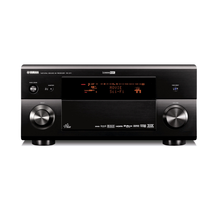
Page 4: Front Panels
RX-Z11/DSP-Z11 I FRONT PANELS RX-Z11 (U, C models) U model C model DSP-Z11 (R, T, K, B, G, E, L models) - Page 5 RX-Z11/DSP-Z11 RX-Z11 (A model) DSP-Z11 (J model)
-
Page 6: Rear Panels
RX-Z11/DSP-Z11 I REAR PANELS RX-Z11 (U model) RX-Z11 (C model) - Page 7 RX-Z11/DSP-Z11 RX-Z11 (R model) RX-Z11 (T model)
- Page 8 RX-Z11/DSP-Z11 RX-Z11 (K model) RX-Z11 (A model)
- Page 9 RX-Z11/DSP-Z11 DSP-Z11 (B model) DSP-Z11 (G, E models)
- Page 10 RX-Z11/DSP-Z11 DSP-Z11 (L model) DSP-Z11 (J model)
-
Page 11: Remote Control Panels
• RAV382 • RAV381 RX-Z11 (U, C models) RX-Z11 (R, T, K, A models) DSP-Z11 (J model) DSP-Z11 (B, G, E, L models) • RAV33 RX-Z11 (U, C, R, T, K, A models) DSP-Z11 (B, G, E, L, J models) -
Page 12: Specifications
RX-Z11/DSP-Z11 I SPECIFICATIONS I Audio Section / Minimum RMS Output Power (Power Amp. Section) / Maximum Input Signal Level / (20 Hz to 20 kHz, 0.04 % THD) PHONO (MM) (1 kHz, 0.1 % THD) ......60 mV or more CD, etc. - Page 13 This product is manufactured under license from Neural Audio Corporation and ................ 75 ohms unbalanced THX Ltd. YAMAHA CORPORATION hereby grants the user a non-exclusive, non- transferable, limited right of use to this product under U.S.A. and foreign patent, I AM Section / patent pending and other technology or trademarks owned by Neural Audio Cor- Manufactured under license from Dolby Laboratories.
- Page 14 RX-Z11/DSP-Z11 • Sound Field Parameter CLASSICAL1 CLASSICAL2 LIVE/CLUB ENTERTAINMENT MOVIE DSP Level Dialogue Lift Init. Delay Room Size Liveness Sur. Init. Delay Sur. Room Size Sur. Liveness SB. Init. Delay SB. Room Size SB. Liveness Rev. Time Rev. Delay Rev. Level...
- Page 15 RX-Z11/DSP-Z11 • Sound Field Parameter / SURROUND Music CLASSICAL1 CLASSICAL2 LIVE/CLUB ENTERTAINMENT MOVIE STEREO DECODE Enhancer PS1 presence field Init. delay Room size – – – – – – Liveness – – – – – – – – – –...
- Page 16 RX-Z11/DSP-Z11...
-
Page 17: Internal View
RX-Z11/DSP-Z11 I INTERNAL VIEW • Top view AMPPOW (3) P.C.B. FM / AM tuner (U, C, A models) INPUT (2) P.C.B. SUBCPU (5) P.C.B. AVIDEO (3) P.C.B. SUBCPU (4) P.C.B. DVIDEO (1) P.C.B. SUBCPU (2) P.C.B. DSP P.C.B. AVIDEO (1) P.C.B. -
Page 18: Disassembly Procedures
RX-Z11/DSP-Z11 I DISASSEMBLY PROCEDURES Disconnect the power cable from the AC outlet. The disassembly procedure of this unit is described by sections as follows. • Disassembly procedures of Front section: When removing the front panel and sub-chassis unit When removing the power transformer, POWER (2) and POWER (3) P.C.B.s... - Page 19 RX-Z11/DSP-Z11 Disassembly procedures of Front section 1. Removal of Front Panel Unit a. Remove 6 screws (1), 2 screws (2) and then remove the top cover. (Fig. 1) b. Remove 4 screws (3) and then remove the panel side L. (Fig. 1) c.
- Page 20 RX-Z11/DSP-Z11 3. Removal of Power Transformer a. Remove 2 push rivets (9) and then remove SUBCPU (8) P.C.B.. (Fig. 2) b. Remove screw (0) and then remove the support POW5. (Fig. 2) c. Remove screw (A), CB59 and then remove POWER (6) P.C.B..
- Page 21 RX-Z11/DSP-Z11 Disassembly procedures of Side section ST915 : BLACK 1. Removal of MAIN L P.C.B. ST917 : WHITE CB931 a. Remove 6 screws (1), 2 screws (2) and then remove ST918 : ORANGE MAIN L P.C.B. ST912 : VIOLET the top cover. (Fig. 3)
- Page 22 RX-Z11/DSP-Z11 2. Removal of MAIN R P.C.B. a. Remove 6 screws (1), 2 screws (2) and then remove Caution when replacing power transistors • When replacing power transistors, be sure to replace the top cover. (Fig. 6) 2 of them for each channel as a pair (2SA2121/ b.
- Page 23 RX-Z11/DSP-Z11 U, C models 3. Removal of AMPPOW (2) and INPUT (2) P.C.B.s a. Remove 2 screws (J) and then remove the AM/FM tuner (U, C, A models). (Fig. 9) b. Remove 3 screws (K). (Fig. 10) c. Remove screw (L). (Fig. 9) d.
- Page 24 RX-Z11/DSP-Z11 Disassembly procedures of Rear section 1. Removal of DVIDEO (1) and DSP P.C.B.s PUSH MARK a. Remove 6 screws (1), 2 screws (2) and then remove Hook DVIDEO (1) P.C.B. the top cover. (Fig. 11) CB604 b. Remove 7 screws (3). (Fig. 12) Hook c.
- Page 25 RX-Z11/DSP-Z11 When replacing DSP P.C.B.: a. Remove old DSP P.C.B. from this unit. Shield case HM b. Write down MAC address number, which is printed on a MAC address label attached to old DSP P.C.B.. c. Remove a MAC address label from new DSP AVIDEO (2) P.C.B.
- Page 26 RX-Z11/DSP-Z11 f. Remove 2 screws (D) and then remove the SUBCPU 5. Removal of AVIDEO (1) P.C.B. (5) P.C.B.. (Fig. 16) a. Remove 2 screws (I) and then remove HD radio tuner g. Remove screw (E). (Fig. 16) (U model). (Fig. 17, 19) h.
- Page 27 RX-Z11/DSP-Z11 Disassembly procedures of Bottom section 1. Replacement of fuse a. Remove 5 screws (1) and then remove the cover transformer. (Fig. 20) b. Replace fuses F1 and F2. 2. Removal of DC Fun Motors L/R a. Remove 19 screws (2) and then remove the bottom cover.
- Page 28 RX-Z11/DSP-Z11 3. Removal of POWER (1) and (5) P.C.B. a. Remove 4 screws (5) and then remove the panel side L. (Fig. 21) b. Remove 2 screws (6) and then pull out POWER (5) P.C.B.. (Fig. 21) c. Remove 2 screws (7) and pull out POWER (4) P.C.B..
-
Page 29: Updating Firmware
RX-Z11/DSP-Z11 I UPDATING FIRMWARE / Note) The user memories (sound field parameters, sys- tem memory, tuner presetting, etc.) are kept stored even when you write the firmware. Writing to Main microprocessor When replacing the following parts, be sure to write the latest firmware. - Page 30 Press the “MENU” key and start writing the firmware again. Error display / Contents / The firmware is not applicable to RX-Z11/DSP-Z11. / INVALID FILE The firmware is not written in the USB flash memory or does not exist in the root folder. / NOT FOUND The system software is damaged.
- Page 31 RX-Z11/DSP-Z11 G Confirmation of firmware version and checksum 1. Connect the power cable of this unit to the AC outlet. 2. Press the “MASTER ON/OFF” key of this unit while pressing the “PROGRAM” knob of this unit. Then the ADVANCED SETUP mode is activated.
- Page 32 RX-Z11/DSP-Z11 Writing to Sub-microprocessor When you need to update firmware of the sub-micro- processor, be sure to write the latest firmware. G Required tools • Windows 98/2000/Me/XP, PC with a serial port (RS232C) • Firmware downloader program FlashSta.exe (Ver. 2.0): for microprocessor •...
- Page 33 RX-Z11/DSP-Z11 G Operation Procedures 1. Turn off the power of this unit and disconnect the power cable from the AC outlet. 2. Remove 6 screws (1), 2 screws (2) and then re- move the top cover. (Fig. 1) 3. Set the switch (SW301) of RS232C conversion adapter to the “FLASH UCOM”...
- Page 34 RX-Z11/DSP-Z11 5. Start up “FlashSta.exe”. “Select Program” is displayed. (Fig. 2) 6. Select Program: “Inter flash memory”, RS232C Port: “COMx (serial port of the PC connected to this unit)”. (Fig. 2) 7. Confirm settings and click [OK]. “M16C Flash Start” is displayed in about 5 seconds. (Fig. 2) 8.
- Page 35 RX-Z11/DSP-Z11 12. “ID Check” is displayed. (Fig. 4) Click [Refer...], and select “Z11_SubCPU_Vxxxx.s2”. (Fig. 4) The ID code and MCU type are loaded automatically when the file is selected. (Fig. 4) Click [OK]. (Fig. 4) When [Refer...] is clicked, the open file screen is displayed.
- Page 36 RX-Z11/DSP-Z11 13. Click [E.P.R...], and “Erase OK?” is displayed. (Fig. 5) Click [OK] to start writing. (Fig. 5) 14. When writing is completed, “Program Finished” is displayed. (Fig. 5) Click [OK]. (Fig. 5) 15. Disconnect the power cable of this unit from the AC outlet.
-
Page 37: Self-Diagnostic Function
RX-Z11/DSP-Z11 G Confirmation of firmware version and checksum Confirm the firmware is updated successfully with the self-diagnostic function. For more information, refer to “SELF-DIAGNOSTIC FUNCTION”. 1. Connect the power cable of this unit to the AC out- let. 2. Press the “MASTER ON/OFF” key while simulta- neously pressing the “PROGRAM”... - Page 38 RX-Z11/DSP-Z11 4. Select the self-diagnostic function menu “28-4. All checksum”. Check the displayed checksum is the same as the written firmware checksum. Checksum: xxxx (The checksum value is found where downloading is specified to.) 28.ROM VER/SUM S-SUM.7B When the displayed firmware version and checksum...
- Page 39 RX-Z11/DSP-Z11 MEMO MEMO...
- Page 40 RX-Z11/DSP-Z11 I SELF-DIAGNOSTIC FUNCTION / There are 28 main menu items, each of which has sub- menu items. Listed in the table below are menu items and sub-menu items. MAIN MENU SUB MENU DSP THROUGH MARGIN FULL BIT PLL = OFF...
- Page 41 RX-Z11/DSP-Z11 MAIN MENU SUB MENU MAIN MENU SUB MENU ZONE2, 3, 4 INPUT : CD PLL Lock Check ZONE2, 3, 4 INPUT : TUNER VCXO 22M High limit ZONE2, 3, 4 INPUT : PHONO VCXO 22M Low limit ZONE2, 3, 4 INPUT : XM...
- Page 42 RX-Z11/DSP-Z11 • Starting Self-Diagnostic Function • Display provided when Self-Diagnos- Press the “MASTER ON/OFF” key while simultaneously tic Function started pressing the “PROGRAM” knob and “MENU” key of this The FL display of this unit displays the protection function unit as indicated in the figure below.
- Page 43 RX-Z11/DSP-Z11 When there is a history of protection function due to abnormal voltage in the power supply section DIAGNOSTIC PSx:000 A/D conversion value of voltage Cause: The voltage in the power supply section is abnormal. Supplementary information: The abnormal voltage is displayed in based on 5V as 255.
- Page 44 RX-Z11/DSP-Z11 • History of protection function When the protection function has worked, its history is stored in memory with a backup. Even if no abnormality is noted while servicing this unit, an abnormality which has occurred previously can be defined as long as the backup data has been stored.
- Page 45 RX-Z11/DSP-Z11 • Functions in Self-Diagnostic Function mode In addition to the self-diagnostic function menu items, functions listed below are available. • Input selection, Multi channel input • Center/Rear/Rear center/Sub-woofer level adjust- ment • Muting • Power on/off • Master volume Functions related to the tuner and the set menu are not available.
- Page 46 RX-Z11/DSP-Z11 • Details of Self-Diagnostic Function menu With full-bit output specified in some modes, it is possible to execute 0dBFS output without head margin in each channel. 1. DSP THROUGH This function is for DSP2 only. Main DSP of DSP2 is selected for FRONT output.
- Page 47 RX-Z11/DSP-Z11 DSP THROUGH COAX RX0-4 T*CLK ‚˜ 4 S*CLK S/PDIF SEL Zone2 TDATA ISEL ‚˜ 5 R*CLK MAIN HDMI SPDIF RSEL SDIN DIR/DIT S/PDIF SEL NPGA Jitter absorb PLL Zone2 RDATA ZSEL MCLKO MCLKI LRCKI RECOUT RXOUT BCK/LRCK LRCK DATA DSDCK MAIN 5.1ch...
- Page 48 RX-Z11/DSP-Z11 DSP23 BYPASS 2.BYPASS DSP23 INPUT: DVD ANALOG SPEAKER OUT: 1kHz, SUBWOOFER OUTPUT: 50Hz SPEAKER OUT SUBWOOFER Input level Volume OUTPUT FRONT CENTER SURROUND SURROUND BACK L/R FRONT PRESENCE REAR PRESENCE Both ch, -20 dBm +6.5 dB -∞ dBm -∞ dBm -∞...
- Page 49 RX-Z11/DSP-Z11 DSP123 BYPASS COAX RX0-4 T*CLK ‚˜ 4 S*CLK S/PDIF SEL Zone2 TDATA ISEL ‚˜ 5 R*CLK MAIN HDMI SPDIF RSEL SDIN DIR/DIT S/PDIF SEL NPGA Jitter absorb PLL Zone2 RDATA ZSEL MCLKO MCLKI LRCKI RECOUT RXOUT BCK/LRCK LRCK DATA DSDCK MAIN 5.1ch...
- Page 50 RX-Z11/DSP-Z11 3. HDMI AUDIO The audio signals input to HDMI IN are selected by the sub-menu and output. When selecting DSD or DSD Direct, be sure to connect an HDMI unit with DSD output function. AUTO 3.HDMI AUDIO AUTO DSD Direct DSD (Direct Stream Digital) is output by the direct mode.
- Page 51 RX-Z11/DSP-Z11 The analog switch settings for each sub-menu are as shown in the table below. SUB MENU FL/FR CENTER SL/SR SBL/SBR F. PRES. R. PRES. LFE/B: FRONT LARGE LARGE LARGE FRONT LARGE CENTER MIX LARGE NONE LARGE SWFR LARGE PRESENCE MIX...
- Page 52 RX-Z11/DSP-Z11 5. MULTI CH INPUT It is possible to select the 6ch/8ch input and 6-ohm/8- ohm by using the SUB menu. 6CH INPUT_6-ohm 5.Multi ch IN 6ch INPUT_6Ω INPUT: MULTI CH INPUT SPEAKER OUT: 1kHz, SUBWOOFER OUTPUT: 50Hz SPEAKER OUT...
- Page 53 RX-Z11/DSP-Z11 8CH INPUT_6-ohmSP (Special mode) 5.Multi ch IN 8ch INPUT_6ΩSP INPUT: MULTI CH INPUT SPEAKER OUT: 1kHz, SUBWOOFER OUTPUT: 50Hz SPEAKER OUT SUBWOOFER Input level Volume OUTPUT FRONT CENTER SURROUND SURROUND BACK L/R FRONT PRESENCE REAR PRESENCE Both ch, -20 dBm +6.5 dB...
- Page 54 RX-Z11/DSP-Z11 7. FL CHECK Use this program to check the FL display section. Using the sub-menu operation, the display status of the FL display section vary as follows. For audio signal processing, use EFFECT OFF (L/R output by using ANALOG MAIN BYPASS).
- Page 55 RX-Z11/DSP-Z11 8. MANUAL TEST The built-in noise generator of DSP outputs the test noise through the channels specified by the sub- menu. The noise frequency for LFE is 30 to 80 Hz. Other than that, the noise frequency is 500 to 2 kHz.
- Page 56 RX-Z11/DSP-Z11 9. ZONE TEST ZONE2, 3, 4 INPUT : BD/HD DVD 9.ZONE TEST BD/HD DVD ZONE2, 3, 4 INPUT : DVD 9.ZONE TEST ZONE2, 3, 4 INPUT : DTV 9.ZONE TEST ZONE2, 3, 4 INPUT : CBL/SAT 9.ZONE TEST CBL/SAT ZONE2, 3, 4 INPUT : DVR 9.ZONE TEST...
- Page 57 RX-Z11/DSP-Z11 ZONE2, 3, 4 INPUT : TUNER 9.ZONE TEST TUNER ZONE2, 3, 4 INPUT : PHONO 9.ZONE TEST PHONO ZONE2, 3, 4 INPUT : XM 9.ZONE TEST ZONE2, 3, 4 INPUT : NET/USB 9.ZONE TEST NET/USB ZONE2, 3, 4 INPUT : HD-RADIO 9.ZONE TEST...
- Page 58 RX-Z11/DSP-Z11 11. SYSTEM MONITOR This menu is used to display the A/D conversion value of the main microprocessor which detects panel keys of this unit and protection functions in using the sub- menu. Signal processing is maintained in the status before execution.
- Page 59 RX-Z11/DSP-Z11 FANCNT/FAN speed/MODE The value of TM1/TM2/TM3 is detected and FAN is controled. 11.SYS MONITOR FAN:41% A/L TO THX fan operation / : Normal : THX mode Fan operation / – : STOP L : LOW (60˚C) M : (65˚C) H : HIGH (72˚C)
- Page 60 (Reference voltage: 5V=255) 11.AD CHECK K0:255 K1:255 RX-Z11 (U, C, A models) DSP-Z11 (R, T, K, B, G, E, L models) DSP-Z11 (J model) Display Display...
- Page 61 RX-Z11/DSP-Z11 12. XM STATUS (U, C models) The output check of XM Radio Antenna is executed. 1k -1dB/44.1k The test tone (1kHz, -1dB/44.1kHz) is output. 12.XM TEST 1k - 1dB/44 1k -61dB/44.1k The test tone (1kHz, -61dB/44.1kHz) is output. 12.XM TEST 1k -61dB/44 Mute /44.1k...
- Page 62 RX-Z11/DSP-Z11 ISO Tone/32k The ISO tone (32kHz) is output. 12.XM TEST ISO Tone/32 XM/DT Bus Power: OFF The power of XM module is turned off. 12.XM TEST Bus Power:OFF 13. HD RADIO TEST (U model) CPU version The firmware version is displayed.
- Page 63 RX-Z11/DSP-Z11 14. iPod This menu is used to test the DOCK connector without the iPod itself. After turning off the power to this unit, short between pins No. 14 (TX) and No. 18 (RX), be- tween pins No. 1 (PWR) and No. 17 (ACCPOW) and between pins No.
- Page 64 RX-Z11/DSP-Z11 15. NET CHECK IP Address Check IP address obtained is checked. 15.Net IP CHECK:NG OK: Connected (IP address obtained) NG: No traffic MAC Address Check MAC address information is checked. 15.Net MAC CHECK:OK OK: Normal NG: Unwritten MAC LABEL No SET After replacing DSP P.C.B., restore the MAC address...
- Page 65 RX-Z11/DSP-Z11 b. Turn the “PROGRAM” knob to change the alphanumerical letter in the first digit. 15.Net MAC[1]AxxxA Change b. Press the “PROGRAM” knob to shift to the next digit. 15.Net MAC1[B]xxxA Shift to the next digit Press Press d. Repeat steps b. and c. to change all settings to the MAC address number of the old DSP P.C.B..
- Page 66 RX-Z11/DSP-Z11 LINK CHECK LAN cable connection is checked. 15.Net LINK CHECK:NG OK: Normal NG: Unconnected Ext loopback test This menu is used to test the NETWORK connector. With the power to this unit turned off, short between pins No. 1 (Rx+) and No. 3 (Tx+) of the NETWORK connector.
- Page 67 RX-Z11/DSP-Z11 16. USB CHECK VNP2 TEST 1k 1kHz test tone is output. 16.USB VNP2 TEST 1k VNP2 TEST 20Hz 20Hz test tone is output. 16.USB VNP2 TEST 20Hz VNP2 TEST 20k 20kHz test tone is output. 16.USB VNP2 TEST 20k VNP2 TEST2 1kHz test tone is output.
- Page 68 RX-Z11/DSP-Z11 The music file recorded in the USB flash memory is reproduced. a. Copy the music file from PC into the roof folder of the USB flash memory. b. Insert the USB flash memory to the USB terminal of this unit.
- Page 69 RX-Z11/DSP-Z11 18. THERMAL HIST. The history of thermal protection function is displayed. After selecting the sub-menu, press the “STRAIGHT” key, and the history will be erased. THM : 18.THM HIST. THM : 19. DSP P.C.B. CHECK Whether the bus of DSP P.C.B. is connected properly or not is self-diagnosed.
- Page 70 RX-Z11/DSP-Z11 SPI Check OK : 0 NG : 1 19.DSP CHECK SPI:0000 Error detection of DSP#4 (IC514) / Error detection of DSP#3 (IC510) / Error detection of DSP#2 (IC506) / Error detection of DSP#1 (IC504) / The PLL (Phase Locked Loop) operation is checked.
- Page 71 RX-Z11/DSP-Z11 UART Check Not applied to these models. 19.DSP CHECK UART:NG 20. D-VIDEO P.C.B. CHECK Whether the bus of D-VIDEO P.C.B. is connected properly or not is self-diagnosed. ALL Check The synthetic judgment result is displayed. : No error detected : An error is detected 20.DVIDEO...
- Page 72 The product ID of this unit written in HDMI module is displayed. 311B (U, C, R, T, K, A, B, G, L models) 21.HDMI INFO HPI:311B HDMI Vendor Name The vendor name (YAMAHA) of this unit written in the HDMI module is displayed. 21.HDMI INFO HVN:YAMAHA...
- Page 73 RX-Z11/DSP-Z11 22. DVIDEO ROUTE CHECK The video signal is converted and output as follows. HDMI loopback test Check1 to 4 22.VIDEO ROUTE Check1:NG Check1 Loopback check HDMI Cable for Loopback CB901 CB807 CB808 CB809 CB810 CB812 CB813 HDMI HDMI HDMI...
- Page 74 RX-Z11/DSP-Z11 Check3 Test pattern 720p Y, Cb, Cr 4:2:2 20 bit CB901 CB807 CB808 CB809 CB810 CB812 CB813 HDMI HDMI HDMI HDMI HDMI HDMI HDMI Front OUT1 OUT2 IC901 IC823 IC826 IC827 IC829 IC834 HDMIEQ HDMISW HDMISW HDMITX HDMITX FPGA...
- Page 75 RX-Z11/DSP-Z11 HDMI_480i to HDMI_out1 22.VIDEO ROUTE HDMI 480i rpt CB901 CB807 CB808 CB809 CB810 CB812 CB813 HDMI HDMI HDMI HDMI HDMI HDMI HDMI Front OUT1 OUT2 IC901 IC823 IC826 IC827 IC829 IC834 HDMIEQ HDMISW HDMISW HDMITX HDMITX FPGA CXB1442 SiI9185...
- Page 76 RX-Z11/DSP-Z11 CVBS to DA and HDMI_out1 22.VIDEO ROUTE DIGITAL CVBS CB901 CB807 CB808 CB809 CB810 CB812 CB813 HDMI HDMI HDMI HDMI HDMI HDMI HDMI Front OUT1 OUT2 IC901 IC823 IC826 IC827 IC829 IC834 HDMIEQ HDMISW HDMISW HDMITX HDMITX FPGA CXB1442...
- Page 77 RX-Z11/DSP-Z11 Component_480p to DA and HDMI_out1 22.VIDEO ROUTE D _ Comp.480p CB901 CB807 CB808 CB809 CB810 CB812 CB813 HDMI HDMI HDMI HDMI HDMI HDMI HDMI Front OUT1 OUT2 IC901 IC823 IC826 IC827 IC829 IC834 HDMIEQ HDMISW HDMISW HDMITX HDMITX FPGA...
- Page 78 RX-Z11/DSP-Z11 YGV_I/P to DA and HDMI_out1 22.VIDEO ROUTE YGV I/P CB901 CB807 CB808 CB809 CB810 CB812 CB813 HDMI HDMI HDMI HDMI HDMI HDMI HDMI Front OUT1 OUT2 IC901 IC823 IC826 IC827 IC829 IC834 HDMIEQ HDMISW HDMISW HDMITX HDMITX FPGA CXB1442...
- Page 79 RX-Z11/DSP-Z11 23. AVIDEO CHECK The video signal is converted and output as follows. ANALOG BYPASS 23.AVIDEO ANALOG BYPASS ANALOG BYPASS DVIDEO P.C.B. Video Decoder Video Decoder ADV7802 ADV7342 IC801 IC802 Freq Counter IC103 MONITOR OUT INPUT Bypass Selector Selector IC102...
- Page 80 RX-Z11/DSP-Z11 VFMUTE CHECK MUTE signals “N_FMUTE” (35pin) and “N_VFMUTE” (53pin) are output from the sub-microprocessor (SUBCPU P.C.B. IC100). 23.AVIDEO VFMUTE CHECK MUTE CHECK MUTE signals “MON_N_VMT” (AE4) and “Z2_N_VMT” (AD4) are output from the main microprocessor (DSP P.C.B. IC704) and MUTE signal “VR_N_VMT (16pin)”...
- Page 81 RX-Z11/DSP-Z11 OSD character pattern (0-127) 23.AVIDEO OSD1 OSD character pattern (0-127) DVIDEO P.C.B. Video Decoder Video Decoder ADV7802 ADV7342 IC801 IC802 Freq Counter IC103 MONITOR OUT INPUT Bypass Selector Selector IC102 IC101 ZONE2 Bypass Selector Selector ZONE2 OUT IC102 IC101...
- Page 82 RX-Z11/DSP-Z11 TEST PATTERN 23.AVIDEO TEST PATTERN Test pattern DVIDEO P.C.B. Video Decoder Video Decoder ADV7802 ADV7342 IC801 IC802 Freq Counter IC103 MONITOR OUT INPUT Bypass Selector Selector IC102 IC101 ZONE2 Bypass Selector Selector ZONE2 OUT IC102 IC101 Bypass Selector INPUT...
- Page 83 RX-Z11/DSP-Z11 25. SET INFO The informations of the model name and destination are displayed. MODEL: RX-Z11, DSP-Z11 RX-Z11 (U, C, A models) DSP-Z11 (J model) DSP-Z11 (R, T, K, B, G, E, K models) 25.SET INFO MODEL:RX-Z11 DEST.: UC, R, T, K, A, BGE, L UC, R, T, K, A, BGE or L is displayed.
- Page 84 RX-Z11/DSP-Z11 27. FACTORY PRESET This menu is used to reserve and inhibit initialization of the user memory. The signals are processed using EFFECT OFF. (The L/R signal is output using ANA- LOG MAIN BYPASS.) PRESET INHIBIT (Initialization inhibited) / User memory initialization is not executed. Select this sub-menu to protect the values set 27.FAC PRESET...
- Page 85 RX-Z11/DSP-Z11 28. ROM VER/SUM The version and checksum are displayed. The signal is processed using EFFECT OFF. The checksum is obtained by adding the data at every 8 bits for each program area and expressing the result as a 4-figure hexadecimal data.
-
Page 86: Amp Adjustment
RX-Z11/DSP-Z11 I AMP ADJUSTMENT Perform all adjustments with no signal applied. G Idling Current Adjustment 1. Turn all the semi-fixed variable resisters for idling current adjustment counterclockwise fully. 2. Turn on the power to this unit and wait for 3 minutes. - Page 87 RX-Z11/DSP-Z11 • MAIN R P.C.B. I dling current adjustments/ DC offset confirmations/ Item Test Point Adjustment Point Rating Test Point Rating DC 8 ±4 mV Center CB921 pin1-pin3 VR912 ST912-ST915 DC 8 ±4 mV Surround R CB924 pin1-pin3 VR915 ST913-ST915 DC 8 ±4 mV...
- Page 88 RX-Z11/DSP-Z11 • SCHEMATIC DIAGRAM MAIN L...
- Page 89 RX-Z11/DSP-Z11 • SCHEMATIC DIAGRAM MAIN R...
-
Page 90: Display Data
RX-Z11/DSP-Z11 I DISPLAY DATA G V4002 : 31-BT-01GN (OPERATION P.C.B.) PATTERN AREA G PIN CONNECTION Pin No. 136 135 133 132 131 Connection F1 F1 Pin No. 130 129 128 127 126 125 124 123 122 121 120 119 118 117 116 115 114 113 112 111 110 109 108 107 106 105 104 103 102 101 100 99 Connection Pin No. - Page 91 RX-Z11/DSP-Z11 G ANODE CONNECTION 1GA-14GA 15GA 16GA 1GB-14GB 15GB 1-1A 1-1B 2-1A 2-1B 3-1A 3-1B 4-1A 4-1B 5-1A 5-1B 1-2A 1-2B 2-2A 2-2B 3-2A 3-2B 4-2A 4-2B P10A 5-2A P10B 5-2B P11A 1-3A P11B 1-3B P12A 2-3A P12B 2-3B P13A...
-
Page 92: Ic Data
RX-Z11/DSP-Z11 I IC DATA IC704: YTD446 (VNP2, DSP P.C.B.) Main microprocessor Network audio equipment, and an equipment with network function * No replacement part available. / GPIO Memory I/F Interrupt ARM926EJ-S Controller Memory ARM9EJ-S Controller0 Dual Timer0 UART0 I-cache D-cache... - Page 93 RX-Z11/DSP-Z11 Function Name Port Name Detail of Function (P.C.B.) nRESET System reset terminal XI_S System clock crystal oscillation terminal XO_S System clock crystal oscillation terminal AE24 XI_A Audio clock crystal oscillation terminal AD24 XO_A Audio clock crystal oscillation terminal TEST0...
- Page 94 RX-Z11/DSP-Z11 Function Name Port Name Detail of Function (P.C.B.) RXD1/AGPIO[6] CPU_MISO(_3) Communication between micro-processors (asynchronous) nCTS1/AGPIO[10] DEV_N_RST Reset output for EtherNET PHY Reset output for NPGA nRTS1/AGPIO[7] V_PON(_3) Video power control (ON/OFF) nDCD1/AGPIO[8] IPD_PON(_3) iPod power control (ON/OFF) nDSR1/AGPIO[13] Z2_N_VMT(_3)
- Page 95 RX-Z11/DSP-Z11 Function Name Port Name Detail of Function (P.C.B.) AD16 USBM USB data- AB16 USB_PWREN USB power enable AC17 USB_OC USB excess current detect AE12 MAC_REF_CLK RMII clock output AE13 MAC0_RXD0 RMII reception data AD13 MAC0_RXD1 RMII reception data AC13...
- Page 96 RX-Z11/DSP-Z11 IC100: M38039FFLHP (SUBCPU P.C.B.) Sub-microprocessor Single chip 8-bit microprocessor Main Main clock clock Sub-clock Sub-clock input output input output Reset input RESET COUT Data bus MICROPROCESSOR Clock generating circuit Timer 1 (8) Prescalar 12 (8) Timer 2 (8) Prescalar X (8)
- Page 97 RX-Z11/DSP-Z11 Function Name Port Name Detail of Function (P.C.B.) P6-2/AN2 (MODEL) Model discrimination by AD value (reserve) P6-1/AN1 KEY1 KEY1 AD value intake P6-0/AN0 KEY0 KEY0 AD value intake P5-7/INT3 PSW_DET Main/Zone2/3/4 power key interrupt FAN_CTRL FAN revolution control P5-6/PWM...
- Page 98 PS protection detect 3 (digital/video power source) Standby --- All Zone power OFF, Master ON MCUSleep --- Low current consumption state at Master OFF Key Input(A-D) Pull-Up Resistance 10 k-Ohms RX-Z11 (U, C, A models) Ohm [V] 0.0 [– 0.3] +1.2k [– 0.7] +1.2k [–...
- Page 99 RX-Z11/DSP-Z11 IC743: MB87L8760 (NPGA1, DSP P.C.B.) Gate array LSI Function Name Port Name Detail of Function (P.C.B.) PIO[0] DSP_N_INT Interrupt from initial stage of TI (DA70Y) PIO[1] PHY_N_INT Interrupt from ether NET PHY (Reserve) PIO[2] DIR_N_INT Interrupt input from DIR...
- Page 100 RX-Z11/DSP-Z11 Function Name Port Name I/O [OFF] Detail of Function (P.C.B.) TXD0 XM_MOSI XM Radio asynchronous serial data transmission RXD0 XM_MISO XM Radio asynchronous serial data reception PI4_XCTS0 TUN_N_TUND TUNER TUNED input PO4_XRTS0 FL_N_RST Reset for FL driver PIO[25] SPI_RDY3...
- Page 101 RX-Z11/DSP-Z11 Function Name Port Name I/O [OFF] Detail of Function (P.C.B.) A[5] SA[5] HOST I/F address bus A[4] SA[4] HOST I/F address bus PI0_MCLKI SEL_MCK MCK input for jitter reduction PLL PI1_LRCK GA_LRCK LRCK (DSDCK) input for jitter reduction PLL...
- Page 102 RX-Z11/DSP-Z11 IC653: MB87L8760 (NPGA2, DVIDEO P.C.B.) Gate array LSI Function Name Port Name Detail of Function (P.C.B.) PIO[0] VDEC_N_INT Interrupt signal from video decoder (Reserve) PIO[1] N_P_SEL OSD crystal select : NTSC (High), PAL (Low) / Processing for V_PON (VNP2: AGPI0[7]) OFF time is required because connection is to video system.
- Page 103 RX-Z11/DSP-Z11 Function Name Port Name I/O [OFF] Detail of Function (P.C.B.) VOL_MOSI Serial data output for main volume (NJW1195) control Serial data output for zone volume (NJW1194) control Serial data output for mix analog switch (NJU7313) control / ES correction required : 3.3V to 5.0V conversion required...
- Page 104 RX-Z11/DSP-Z11 Function Name Port Name I/O [OFF] Detail of Function (P.C.B.) TEST2 TEST2 For TEST PO1_XLOCK MIX_N_CS MIX analog SW (NJU731X)/Chip select XPCO FPGA_N_CS Chip select for FPGA control VIPC_N_CS Video I/P conversion device/Chip select PO0_MCLKO – / ES correction required : 3.3V to 5.0V conversion required...
- Page 105 RX-Z11/DSP-Z11 • Expansion port IC161 : NJW1321FP1 (AVIDEO P.C.B.) I/O expander for microcontroller IC371, 372 : NJW1321FP1 (SUBCPU P.C.B.) I/O expander for microcontroller Serial/parallel converter/shift register DOUT CLK# RES# I/O control/output register port 0 I/O buffer port 1 I/O buffer...
- Page 106 RX-Z11/DSP-Z11 LC709004A (AEX2) Function Name Port Name I/O [OFF] Detail of Function (P.C.B.) PIO0 TUN_MT TUNER mute output PIO1 Z4_N_FMT Full mute zone 4 PIO2 Z3_N_FMT Full mute zone 3 PIO3 Z2_N_FMT Full mute zone 2 PIO4 MONO_Z4 Zone 4 mono control / High: MONO...
- Page 107 RX-Z11/DSP-Z11 IC101, 102: NJW1321FP1 (AVIDEO P.C.B.) Decoder/Post processor Y/R IN1 Y/R OUT1 Y/R IN2 Y/R IN3 Y/R IN4 Y/R OUT2 Pb/G IN1 Pb/G OUT1 Pb/G IN2 Pb/G IN3 Pb OUT2 Pb/G IN4 Pb/G OUT2 Pr IN4 PORT0 PORT1 Y IN3...
-
Page 108: Pin Connection Diagrams
RX-Z11/DSP-Z11 I PIN CONNECTION DIAGRAMS • ICs BA15218F ADM222ARZ ADV7172KST ADV7180BSTZ ADV7802BSTZ-150 BD6517F-E2 ADV7342BSTZ D710E001BZDH300 BD3508EKN-E2 BD9011EKN-E2 CXB1442AR-T4 D70YE101BRFP266 DSD1796DBR F2621E-01-TR NJU7311AM NJU7312AM NJU7313AM PCM1804DBR FHP3350IM14X IP00C772 IP101ALF K4S643232H-UC60000 TC74VHC125FT IS42S32400D-7TL W9864G2GH-7... - Page 109 RX-Z11/DSP-Z11 LA7106M-TLM-E LA73050-TLM-E LB1836M-TLM-E LC709004A-TLM-E PCA9517DP PQ200WNA1ZPH PT6302LQ-008 R1130H181B-TI-F R1171J331D-T1-F R1172S121D-E2-F R1172S181B-E2-F MM74HC4051SJX TC74VHCT08AFT LC74782JM-8A16-TLMC R1130H331B-T1-F LA73053-TLM-E R1172S251B-E2-F MM74HC4053SJX TC74VHCU04FT R1172S331B-E2-F PCM1781DBQR SN74CB3Q3257PWR SN74LS151NSR RH5RE58AA-T1-FA SN74AHCT00PWR SN74AHCT1G32DCKR SN74LVC74APWR SN74LVU04APWR LC89057W-VF4AD-E LM4562MAX LM61CIZ LP2995MX M24256-BRDW6TP 1: Vin 2: GND NJM4565M 3: Vout...
- Page 110 RX-Z11/DSP-Z11 • Diodes • Transistors 2N5401C-AT/P 2N5401C-AT 2N5551S-RTK 2SA1036K 2SA1708 1N4002S D2SBA20 D4SBS6-7101 D15XBN20 2N5551C-AT 2SA1037K 2SC3906K 2SC4488 1SS133 D30XBN20-7000 2SA970 2SA1145 2SA1587-GR 2SK3288ENTL-E 1SS176 Anode 2SC2705 2SC3837K KTA1504S MTZJ6.8B 2SC4117-GR KTA1517S MTZJ10B KTC3875S KTC3911S – – – Cathode 2SA2168...
-
Page 111: Block Diagrams
RX-Z11/DSP-Z11 I BLOCK DIAGRAMS AUDIO/VIDEO SECTION BLOCK DIAGRAM Audio Block Diagram COAXIAL DIGITAL IN ZONE2/REC OUT (COAXIAL DIGITAL) ZONE OUT / DVR Video Block Diagram BD/HD DVD * REC OUT: J model * ZONE2/REC OUT: U, C, R, T, K, A, B, G, E, L models... - Page 112 RX-Z11/DSP-Z11 AUDIO (ANALOG/AMP) SECTION BLOCK DIAGRAM • See page 165 → FUNCTION (2) INPUT (1) SCHEMATIC DIAGRAM • See page 163 → SCHEMATIC DIAGRAM HP relay IC258 IC263 IC340 NJU7313 analog-switch To OPERATION (2) Main Zone Location : IC350 RY308...
- Page 113 RX-Z11/DSP-Z11 AUDIO (DIGITAL) SECTION BLOCK DIAGRAM IC263 Main ADC FUNCTION (2) • See page 166 → • See page 159-161 → INPUT (2) ADC_MCK SCKI ADC_BCK • See page 163 → SCHEMATIC DIAGRAM SCHEMATIC DIAGRAM ADC_LRCK LRCK ADC_SDO SCHEMATIC DIAGRAM...
- Page 114 RX-Z11/DSP-Z11 VIDEO SECTION BLOCK DIAGRAM FPGA_SCK This block is not related with "V PON" DVIDEO (1) FPGA_MOSI FPGA_N_CFG FPGA_CDONE FPGA_MISO D[35-24] FPGA_N_CS FPGA_N_STA D[23-12] • See page 176-178 → D[11-0] HDMI_SDA HEQ_SDA HDMI HEQ_N_RST HDMI_SCL HEQ_SCL HRX_27MHz HRX_N_RST SCHEMATIC DIAGRAM...
- Page 115 RX-Z11/DSP-Z11 MAIN POWER SUPPLY SECTION BLOCK DIAGRAM • See page 169 → • See page 171 → PCB-SUBCPU (1) PCB-POWER (1) POWER (1) SUBCPU (1) Control Block Diagram (SUBCPU) SCHEMATIC DIAGRAM SCHEMATIC DIAGRAM PCB-DVIDEO IC xx [HDMI Interface Block] DEST +1.8H...
- Page 116 RX-Z11/DSP-Z11 DIGITAL POWER SUPPLY SECTION BLOCK DIAGRAM CB622 CB622 CB622 CB627 CB502 +4.3DSW +6.3DSW +2.8DSW +12RY +2.0DSW PCB DVIDEO PCB DSP PCB DVIDEO-2 DVIDEO L6205 +4.3H L8031 Wire Front HDMI L6201 Audio PLL • See page 176-179 → B to B...
- Page 117 RX-Z11/DSP-Z11 SYSTEM CONTROL SECTION BLOCK DIAGRAM PCB SUBCPU-1 SUBCPU (1) RS232C • See page 171 → REMOTE IN IC82 SCHEMATIC DIAGRAM Driver PCB OPE PCB DSP ADM222ARZ OPERATION CB701 Connector PCB OPE • See page 164 → Pulse from Rotary Encoder...
- Page 118 RX-Z11/DSP-Z11 DSP SECTION BLOCK DIAGRAM CB696 CB562 REAR USB IC508 IC505 SDRAM SDRAM IC561 ETHERNET IC506 IC504 IC541 DSP #2 DSP #1 Audio data DA70Y DA710 LC89057W IC704 IC697 IC703 MAIN MICROPROCESSOR SEL. SDRAM 128Mbit YTD446 VNP2 24.576MHz 5.00MHz IC510...
- Page 119 RX-Z11/DSP-Z11 SUB_CONTROL SECTION BLOCK DIAGRAM SUBCPU (5) • See page 165 → INPUT (1) • See page 172 → SCHEMATIC DIAGRAM Tuner pack SCHEMATIC DIAGRAM U, C, A models IC704 Main Input selector TUN_SCK MAIN /Rec Out (Front) TUN_N_CS MICRO-...
-
Page 120: Printed Circuit Boards
RX-Z11/DSP-Z11 I PRINTED CIRCUIT BOARDS • Semiconductor Location Ref no. Location Ref no. Location Ref no. Location Ref no. Location Ref no. Location Ref no. Location Ref no. Location Ref no. Location Ref no. Location Ref no. Location D5003 IC505... - Page 121 RX-Z11/DSP-Z11 DSP P.C.B. (Side B) CB784 CB785 • Semiconductor Location Ref no. Location D5001 D5002 D6960 SUBCPU (4) D6961 (CB379) SUBCPU (4) D7401 (CB387) D7402 D7403 D7404...
- Page 122 RX-Z11/DSP-Z11 FUNCTION (1) P.C.B. (Side A) U, C, R, T, K, A, B, G, E, L models MULTI CH INPUT ZONE OUT PRE OUT SB (8 CH) SURROUND ZONE 2 ZONE 3 ZONE 4 FRONT SURROUND CENTER SUR.BACK FRONT REAR...
- Page 123 RX-Z11/DSP-Z11 FUNCTION (1) P.C.B. (Side B) U, C, R, T, K, A, B, G, E, L models • Semiconductor Location Ref no. Location Ref no. Location D3009 Q3042 D3010 Q3055 D3011 Q3056 D3012 Q3057 D3013 Q3059 D3014 Q3060 D3015 Q3061...
- Page 124 RX-Z11/DSP-Z11 FUNCTION (2) P.C.B. (Side A) SUBCPU (2) (CB378) SUBCPU (4) SUBCPU (4) (CB386) (CB380) CB254 CB255 CB256 +3.3HD HDRDS POWER (2) IC258 MAD_N_RST VOUT (CB56) ZAD_N_RST ZDAC_MUT +12T HDRD_MUT HDRD_N_RST HDRD_MISO IC260 IC261 IC259 HRDD_MOSI HDRD_SPDIF SUBCPU (5) (CB372)
- Page 125 RX-Z11/DSP-Z11 FUNCTION (2) P.C.B. (Side B) U, C, R, T, K, A, B, G, E, L models U, C models U, C, R, T, K, A, B, G, E, L models • Semiconductor Location Ref no. Location D2505 D2506 D2507...
- Page 126 RX-Z11/DSP-Z11 OPERATION (1) P.C.B. (Side A) OPERATION (2) (CB458) U, C, A models U, C, R, T, K, A, B, G, E, L models W4001 ZONE ON/OFF ZONE CONTROLS ZONE 2 ZONE 3 ZONE 4 REC OUT/ TONE ZONE 2...
- Page 127 RX-Z11/DSP-Z11 OPERATION (1) P.C.B. (Side B) U, C, R, T, K, A, B, G, E, L models IC403 49 48 16 17 • Semiconductor Location Ref no. Location Ref no. Location D4001 IC403 D4002 IC404 D4003 Q4006 D4004 Q4008 D4005...
- Page 128 RX-Z11/DSP-Z11 OPERATION (2) P.C.B. (Side A) OPERATION (2) P.C.B. (Side B) PHONES OPTIMZER VIDEO AUX SILENT CINEMA S VIDEO VIDEO AUDIO OPTICAL U, C, R, T, K, A, B, G, E, L models J model JK453 JK452 JK451 IC451 W4502...
- Page 129 RX-Z11/DSP-Z11 OPERATION (5) P.C.B. (Side A) OPERATION (5) P.C.B. (Side B) OPERATION (6) P.C.B. (Side A) OPERATION (6) P.C.B. (Side B) MASTER MAIN ZONE ON/OFF PROGRAM W4503 M_SW MAIN_ZONE OPERATION (2) (CB459) OPERATION (7) P.C.B. OPERATION (7) P.C.B. (Side A)
- Page 130 RX-Z11/DSP-Z11 INPUT (1) P.C.B. (Side A) AUDIO IN AUDIO OUT AUDIO IN PHONO TUNER MD/TAPE CD-R MD/TAPE CD-R CBL/SAT L / R L / R L / R L / R L / R L / R L / R...
- Page 131 RX-Z11/DSP-Z11 INPUT (1) P.C.B. (Side B) R, T, K, B, G, E, L, J models • Semiconductor Location Ref no. Location D2001 D2002...
- Page 132 RX-Z11/DSP-Z11 INPUT (2) P.C.B. (Side A) (CB541) COAX0 SPD_ISEL0 COAX1 SPD_ISEL1 COAX2 U, C models SPD_ISEL2 COAX3 SPD_RSEL0 ISEL_OUT SPD_RSEL1 RSEL_OUT REC_SPDIF SPD_RSEL2 DIT_SPDIF OPT_N_INH HDMI_SPDIF IC558 SPD_ZSEL0 HDRD_SPDIF SPD_ZSEL1 SPD_ZSEL2 AUX_SPDIF +3.3D +6.3V +6.3V XM_PON XM_PRT XM_REV XM_LINK XM_MOSI...
- Page 133 RX-Z11/DSP-Z11 INPUT (2) P.C.B. (Side B) U, C models U, C models...
- Page 134 RX-Z11/DSP-Z11 • Semiconductor Location Ref no. Location Ref no. Location Ref no. Location Ref no. Location Ref no. Location Ref no. Location Ref no. Location Ref no. Location Ref no. Location Ref no. Location Ref no. Location Ref no. Location...
- Page 135 RX-Z11/DSP-Z11 • Semiconductor Location Ref no. Location Ref no. Location Ref no. Location Ref no. Location Ref no. Location Ref no. Location Ref no. Location Ref no. Location Ref no. Location Ref no. Location Ref no. Location Ref no. Location Ref no.
- Page 136 RX-Z11/DSP-Z11 • Semiconductor Location Ref no. Location Ref no. Location Ref no. Location Ref no. Location Ref no. Location Ref no. Location Ref no. Location Ref no. Location Ref no. Location Ref no. Location Ref no. Location Ref no. Location Ref no.
- Page 137 RX-Z11/DSP-Z11 • Semiconductor Location Ref no. Location Ref no. Location Ref no. Location Ref no. Location Ref no. Location Ref no. Location Ref no. Location Ref no. Location Ref no. Location Ref no. Location Ref no. Location Ref no. Location Ref no.
- Page 138 RX-Z11/DSP-Z11 POWER (1) P.C.B. POWER (1) P.C.B. (Side A) (Side B) POWER PRIMARY TRANSFORMER CONNECTOR U, C, R, T, A, B, G, E, L, J models BROWN POWER (5) (W1A)(W2A) BROWN BROWN R, T, K, A, B, L, J models...
- Page 139 RX-Z11/DSP-Z11 POWER (2) P.C.B. (Side A) POWER (2) P.C.B. (Side B) POWER (6) (CB59) DVIDEO (1) (CB628) POWER TRANSFORMER W553 W554 CB51 INPUT (1) (W2002) AGreturn AGreturn AGreturn INPUT (1) (W2003) +12T AGreturn -7A1 +7A1 FUNCTION (1) -12A1 (W3004) +12A1 AGSense1 +3.3HDR...
- Page 140 RX-Z11/DSP-Z11 POWER (3) P.C.B. (Side A) POWER (3) P.C.B. (Side B) AMPPOW (1) -12RY (W121) +12RY POWER TRANSFORMER GRAY DVIDEO (1) (CB622) DGRreturn DGRreturn DGRreturn AVIDEO (3) (CB71) PS3_PRT IC55 +6.3DSW +5STBY PS2_PRT PS3_PRT V_PON IPD_PON DGsense +12RY • Semiconductor Location Ref no.
- Page 141 RX-Z11/DSP-Z11 POWER (4) P.C.B. POWER (4) P.C.B. POWER (5) P.C.B. POWER (5) P.C.B. (Side A) (Side B) (Side A) (Side B) R, L models R, L models U, C, R, T, A, B, G, E, L, J models U, C, R, T, A, B, G, E, L, J models...
- Page 142 RX-Z11/DSP-Z11 +5.6M AMPPOW (1) P.C.B. (Side A) PRY1_CTRL PRY2_CTRL POWER (1) PWR_DET (CB1) SCPU_N_RST MAIN L (1) MAIN R (1) MAIN R (1) DEST (ST916) (ST916) (ST915) +12RY AMPPOW (3) (W128B) -12RY SPRY_F+ +5STBY SPRY_FB+ +12RY SPRY_Z2+ +5.6M SPRY_SB+ SPRY_SR+...
- Page 143 RX-Z11/DSP-Z11 AMPPOW (1) P.C.B. (Side B) • Semiconductor Location Ref no. Location Ref no. Location D101 D117 D105 D118 D106 D119 D107 Q119 D108 Q120 D112 Q121 D113 Q123 D114 Q124 D115 Q129 D116 Q130...
- Page 144 RX-Z11/DSP-Z11 AMPPOW (2) P.C.B. (Side A) AMPPOW (2) P.C.B. (Side B) AMPPOW (4) (W201) MAIN L (1) (ST912) CB21 AMPPOW (1) (W127A) THM2 +5STBY W202 SPRY_SB+ W115B AMP_OLV2 DC2_PRT SPRY_PR+ SPRY_SR+ SPRY_Z2+ SPRY_FB+ SPRY_F+ -12RY MAIN L (1) (ST913) W203...
- Page 145 RX-Z11/DSP-Z11 • Semiconductor Location Ref no. Location Ref no. Location Ref no. Location D251 D256 D261 AMPPOW (3) P.C.B. (Side A) AMPPOW (3) P.C.B. (Side B) D252 D257 D262 D253 D258 D263 D254 D259 IC31 D255 D260 AMPPOW (5) MAIN R (1)
- Page 146 RX-Z11/DSP-Z11 SUBCPU (1) P.C.B. (Side A) SUBCPU (1) P.C.B. (Side B) Note) Replacing IC81 EEPROM will clear the user memory (sound field parameters, system memory, tuner presetting, etc.) +5STBY +12RY SPRY_SB FAN_CTRL SPRY_F SPRY_C SPRY_SR SPRY_Z2 SPRY_PR SPRY_FB AMP_N_PON AMP_LMT PS1_PRT •...
- Page 147 RX-Z11/DSP-Z11 SUBCPU (2) P.C.B. (Side A) SUBCPU (2) P.C.B. (Side B) U model HDRD_MISO HDRD_MOSI HDRD_N_RST HDRD_SPDIF HDRD_MISO HDRD_MOSI +3.3HD HDRD_N_RST HDRD_SPDIF +3.3HD +3.3HD HDRDL +3.3HD HD_A_REF +12T HDRDR HDRDG HD_A_REF +12T HDRDR +3.3HD +3.3DA HD RADIO TUNER +12T FUNCTION (2)
- Page 148 RX-Z11/DSP-Z11 SUBCPU (4) P.C.B. (Side A) SUBCPU (4) P.C.B. (Side B) DSD_DR0 DSD_DL0 DSD_DR1 INPUT (1) DSD_DL1 DSD_DR2 (CB207) DSD_DL2 DSDCK (CB785) FUNCTION (2) (CB256) ADC_SD0 ADC_LRCK ADC_BCK AD_SD0 ADC_MCK AD_LRCK ZAD_SD0 AD_BCK ZAD_RCK AD_MCK ZAD_BCK ZAD_SD0 ZAD_MCK ZAD_LRCK VNP_SD0...
- Page 149 RX-Z11/DSP-Z11 SUBCPU (5) P.C.B. (Side A) SUBCPU (5) P.C.B. (Side B) TUNER (U, C, A models) AVIDEO (2) (W1053) U, C, A models U, C, A models U model CB377 CB376 CB371 CB374 U model (CB786) CB372 INPUT (1) (CB204)
- Page 150 RX-Z11/DSP-Z11 SUBCPU (6) P.C.B. (Side A) DVIDEO (1) (CB629) FUNCTION (1) (W3001) CB993 CB992 OPERATION (2) (W4502) HP_N_DET MIC_N_DET PRG_RB PRG_RA ISEL_RB ISEL_RA VOL_RB VOL_RA FL2_N_CS FL1_N_CS AEX_SCK AEX_MOSI GNERAL FL_N_RST PD_LED EM_N_RST REM1_IN PSW_DET KEY1 KEY0 +3.3D M_SW OPERATION (1) (CB401) SUBCPU (6) P.C.B.
- Page 151 RX-Z11/DSP-Z11 SUBCPU (7) P.C.B. (Side A) AVIDEO (2) INPUT (1) (W1051) (W2001) CB995 CB994 +12A1 -12A1 +5D1 (CB695) OPERATION (2) +Data (CB460) -Data AUXL VBus AUXR DGND DVIDEO (1) DGND (CB805) +5D1 +4.3H DVIDEO (2) +Data (CB904) -Data VBus DGND...
- Page 152 RX-Z11/DSP-Z11 J model AVIDEO (1) P.C.B. (Side A) COMPONENT VIDEO D5 VIDEO COMPONENT VIDEO BD/HD DVD CBL/SAT BD/HD DVD CBL/SAT MONITOR MONITOR J model • Semiconductor Location Ref no. Location Ref no. Location Ref no. Location Ref no. Location D702...
- Page 153 RX-Z11/DSP-Z11 AVIDEO (1) P.C.B. (Side B) J model • Semiconductor Location Ref no. Location Ref no. Location D701 D1151 D704 D1152 D705 D1301 D708 D1302 D709 IC112 D710 Q1003 U, C, R, T, K, A, B, G, E, L models AVIDEO (3) P.C.B.
- Page 154 RX-Z11/DSP-Z11 U, C, R, T, K, A, B, G, E, L models AVIDEO (2) P.C.B. (Side A) ZONE OUT VIDEO OUT VIDEO IN COMPONENT VIDEO VIDEO MONITOR CBL/SAT S VIDEO/ S VIDEO/ S VIDEO/ S VIDEO/ S VIDEO/ S VIDEO/...
- Page 155 RX-Z11/DSP-Z11 AVIDEO (2) P.C.B. (Side B) U, C, R, T, K, A, B, G, E, L models • Semiconductor Location Ref no. Location Ref no. Location U, C, R, T, K, A, B, G, E, L models U, C, R, T, K, A, B, G, E, L models...
- Page 156 RX-Z11/DSP-Z11 • Semiconductor Location HDMI (Rear) Ref no. Location Ref no. Location Ref no. Location Ref no. Location DVIDEO (1) P.C.B. (Side A) OUT 2 OUT 1 D6001 D8029 D8078 IC819 CBL/SAT BD/HD DVD D8003 D8030 D8079 IC820 D8004 D8031...
- Page 157 RX-Z11/DSP-Z11 DVIDEO (1) P.C.B. (Side B) • Semiconductor Location Ref no. Location Ref no. Location Ref no. Location D8002 D8088 IC840 IC844 D8012 D8092 IC841 D8013 D8094 IC842 D8023 IC651 IC843 D8024 IC652 IC844 D8025 IC804 IC845 D8027 IC806 IC846...
- Page 158 RX-Z11/DSP-Z11 DVIDEO (2) P.C.B. DVIDEO (2) P.C.B. (Side A) (Side B) USB (Front) HDMI IN (Front) CB903 CB901 +Data IC902 -Data DGND VBus DGND +4.3H CB902 SUBCPU (7) (CB997) SUBCPU (7) (CB998) DVIDEO (1) (CB806) • Semiconductor Location Ref no. Location Ref no. Location...
-
Page 159: Schematic Diagrams
RX-Z11/DSP-Z11 SCHEMATIC DIAGRAMS DSP 1/3 DSP #1 IC501: TC7SH08FU 2-input AND gate IN B IN A DAC/SW OUT Y DASB DIGITAL IN IC505: W9864G2GH-7 IC503, 512, 513: SN74LVC245APWR IC505, 515: BD3508EKN-E2 128/64 M SDRAM Octal bus transceivers with 3-state outputs... - Page 160 RX-Z11/DSP-Z11 DSP 2/3 POINT C-3 XL541 (Pin 29 of IC541) POINT E-1 XL701 (T25 of IC704) POINT E-2 E-3 1 / Q2 (B), 2 / Pin 5 of IC713 Q2 (B) Q2 (B) IC713 5pin IC713 5pin MAIN MICROPROCESSOR Power cable ON...
- Page 161 RX-Z11/DSP-Z11 DSP 3/3 CB781 CB782 IC741 IC782 12.0 12.0 IC781 12.0 IC757 GATE ARRAY #1 AD IN (NPGA1) IC755 IC755 12.0 IC747 10.5 IC755 10.4 IC754 10.8 10.4 IC747 DASB DASW Page 171 Page 171 to SUBCPU (4)_CB387 to SUBCPU (4)_CB379...
- Page 162 RX-Z11/DSP-Z11 FUNCTION 1/2 CB302 IC301, 302: NJW1111V IC305-307, 316: NJM2068MD-TE2 9-in 3-out stereo audio selector Dual operational amplifier InB1 InB2 InB3 InB4 InB5 InB6 InB7 InB8 InB9 OutA1 OutB2 OutB3 12.1 IC305 Page 171 D10 –IN + – + –...
- Page 163 RX-Z11/DSP-Z11 FUNCTION 2/2 FUNCTION 1/2 FUNCTION 2/2 Page 172 to SUBCPU (5)_CB372 FUNCTION (2) ZONE DAC 12.3 IC251 IC251 -12.1 (U, C, R, T, K, A, B, G, E, L models) 12.3 IC252 ZONE DAC IC252 -12.1 (U, C models) 12.3...
- Page 164 OPERATION (5) OPERATION (4) W4501B CB458 JK451 detection for AD port CB452 Key input (A/D) pull-up resistance 10 k-ohms RX-Z11 (U, C, A models) +1.2 k +1.2 k +1.8 k +2.7 k +3.3 k +4.7 k +8.2 k +18.0 k ~ 0.3...
- Page 165 RX-Z11/DSP-Z11 INPUT 1/2 IC204, 222, 223, 225, 226, 228, 230, IC201, 202: NJW1111V Page 172 231, 233, 234, 236, 237, 239, 240: NJM5532M-D 9-in 3-out stereo audio selector Dual low noise operational amplifier to SUBCPU (5)_CB374 InB1 InB2 InB3 InB4...
- Page 166 RX-Z11/DSP-Z11 INPUT 2/2 POINT B-1 XL581 (Pin 28 of IC581) (U, C models) CB582 Page 160 to DSP_CB542 (U, C models) XM DT 3.3 3.3 IC581 IC582 IC583 IC555 IC555 IC555 IC555 IC555 IC560 IC555 ZSEL IC560 IC560 IC560 IC560...
- Page 167 RX-Z11/DSP-Z11 MAIN L Page 170 Page 170 Page 170 to AMPPOW (1)_W117A to AMPPOW (1)_W117B to AMPPOW (1)_W117C Page 170 to AMPPOW (2)_W205 MAIN L (1) Page 170 Page 170 to AMPPOW (2)_W203 to AMPPOW (2)_W202 Page 170 Page 170...
- Page 168 RX-Z11/DSP-Z11 MAIN R Page 170 Page 170 Page 170 to AMPPOW (1)_W116A to AMPPOW (1)_W116B to AMPPOW (1)_W116C Page 170 Page 170 Page 170 Page 170 Page 170 Page 170 to AMPPOW (3)_W257 to AMPPOW (3)_W254 to AMPPOW (3)_W256 to AMPPOW (3)_W255...
- Page 169 RX-Z11/DSP-Z11 POWER POWER (5) AC OUTLET AC IN POWER (4) POWER (1) (R, T, K, A, B, G, E, L models) R, L models VOLTAGE SELECTOR VOLTAGE SELECTOR 230-240V 1-2/5-6 220V 2-3/6-7 110V 3-4/7-8 AC9.5 120V 4-5/8-1 12.1 MAIN TRANSFORMER AC32.0...
- Page 170 RX-Z11/DSP-Z11 AMPPOW IC21, 31: LM61CIZ Temperature sensor W202 Page 167 to MAIN L (1)_ST912 IC21 THM SENSER REAR ZONE/ W201 PRESENCE FRONT ZONE/ PRESENCE W203 Page 167 AMPPOW (4) to MAIN L (1)_ST913 SURROUND SURROUND L SUR.BACK/ BI-AMP IC31 W115B...
- Page 171 RX-Z11/DSP-Z11 SUBCPU 1/2 (Writing port) Page 176 to DVIDEO (1)_CB815 (For factory) IC100: M38039FFLHP#U0 Sub-microprocessor Single chip 8-bit microprocessor Main Main clock clock Sub-clock Sub-clock input output input output Reset input COUT RESET Data bus MICROPROCESSOR Clock generating circuit Timer 1 (8)
- Page 172 RX-Z11/DSP-Z11 SUBCPU 2/2 Page 162 Page 176 G10 to FUNCTION (1)_W3001 to DVIDEO (1)_CB629 CB999 SUBCPU (5) CB991 Page 161 ANTENNA-1 HD-RADIO to DSP_CB786 (U, C, A models) Page 174 to AVIDEO (2)_W1053 W1053 To Tuner Page 165 to INPUT (1)_CB204 -34.3...
- Page 173 RX-Z11/DSP-Z11 AVIDEO 1/3 Page 176 Page 176 Page 176 to DVIDEO (1)_CB801 to DVIDEO (1)_CB802 to DVIDEO (1)_CB803 IC101, 102: NJW1321FP1 Wide band video switch with I C bus Y/R IN1 Y/R OUT1 Y/R IN2 FREQUENCY COUNTER & LPF Y/R IN3...
- Page 174 RX-Z11/DSP-Z11 AVIDEO 2/3 Page 173 to AVIDEO (1)_CB104 CB153 Page 173 -4.8 -4.9 to AVIDEO (1)_W1001 -4.8 W1052 -4.9 Page 169 -4.8 -4.8 to POWER (3)_CB60 SIGNAL DETECT -3.8 -3.8 IC160 IC166 INPUT W1053 Page 172 SELECTOR IC166 to SUBCPU (5)_CB377 W1051 -4.8...
- Page 175 RX-Z11/DSP-Z11 AVIDEO 3/3 AVIDEO 1/3 Page 159 Page 176 to DSP_CB502 to DVIDEO (1)_CB622 IC72 13.7 20.5 No replacement part available. 13.7 No replacement part available. 20.5 20.5 20.5 11.2 AVIDEO 2/3 AVIDEO (3) Page 169 to POWER (3)_CB63 IC72: TC7SZ02FU...
- Page 176 RX-Z11/DSP-Z11 DVIDEO 1/4 DVIDEO (1) CB601 CB604 IC848 IC803 IC804 12.0 12.0 IC849 CB801 Page 173 IC850 to AVIDEO (1)_CB101 IC801 Page 161 Page 161 to DSP_CB781 to DSP_CB782 A/D DECODER POINT C-1 XL803 (Pin 80 of IC801) IC851 IC845...
- Page 177 RX-Z11/DSP-Z11 DVIDEO 2/4 IC805: YGV619 IC806: W9864G2GH-7 OSD display controller 128/64 M SDRAM IC810 IC811 IC812 D31-0 A23-2 CLOCK CSREG BUFFER CSMEM DREQ DRAWING CONTROL SDQ31-0 PROCESSOR SIGNAL INTERFACE UNIT GENERATOR WR2-0 SA12-0 COMMAND DECODER SBA1-0 WAIT SDRAM READY COLUMN DECODER...
- Page 178 RX-Z11/DSP-Z11 DVIDEO 3/4 Page 172 Page 179 HDMI to SUBCPU (7)_W9904 to DVIDEO (2)_CB902 BD/HD DVD CBL/SAT CB806 CB807 CB808 CB809 CB810 CB805 IC854: LB1836M-TLM-E IC831: SN74CB3Q3257PWR IC832: SN74LVC245APWR Motor driver IC IC828, 830: NJM2867F3-05 Octal bus transceivers with 3-state outputs...
- Page 179 RX-Z11/DSP-Z11 DVIDEO 4/4 HDMI IN USB (Front) IC844 IC838 CB901 CB903 DVIDEO (2) IC824 CB904 IC839 Page 172 to SUBCPU (7)_CB997 IC840 IC841 Page 172 to SUBCPU (7)_CB998 CB905 HDMI EQ IC902 IC842 IC901 IC834 IC834 IC834 FPGA FPGA IC903...
- Page 180 RX-Z11/DSP-Z11 I REPLACEMENT PARTS LIST • ELECTRICAL COMPONENT PARTS WARNING G Components having special characteristics are marked s and must be replaced with parts having specifications equal to those originally installed. G The chip resistor is not supplied as a replacement part.
-
Page 181: Replacement Parts List
RX-Z11/DSP-Z11 P.C.B. DSP ✻ New Parts... - Page 182 RX-Z11/DSP-Z11 P.C.B. DSP ✻ New Parts...
- Page 183 RX-Z11/DSP-Z11 P.C.B. DSP ✻ New Parts...
- Page 184 RX-Z11/DSP-Z11 P.C.B. DSP ✻ New Parts...
- Page 185 RX-Z11/DSP-Z11 P.C.B. DSP ✻ New Parts...
- Page 186 RX-Z11/DSP-Z11 P.C.B. DSP and P.C.B. FUNCTION ✻ New Parts...
- Page 187 RX-Z11/DSP-Z11 P.C.B. FUNCTION ✻ New Parts...
- Page 188 RX-Z11/DSP-Z11 P.C.B. FUNCTION ✻ New Parts...
- Page 189 RX-Z11/DSP-Z11 P.C.B. FUNCTION ✻ New Parts...
- Page 190 RX-Z11/DSP-Z11 P.C.B. FUNCTION ✻ New Parts...
- Page 191 RX-Z11/DSP-Z11 P.C.B. FUNCTION and P.C.B. OPERATION ✻ New Parts...
- Page 192 RX-Z11/DSP-Z11 P.C.B. OPERATION ✻ New Parts...
- Page 193 RX-Z11/DSP-Z11 P.C.B. OPERATION and P.C.B. INPUT ✻ New Parts...
- Page 194 RX-Z11/DSP-Z11 P.C.B. INPUT ✻ New Parts...
- Page 195 RX-Z11/DSP-Z11 P.C.B. INPUT ✻ New Parts...
- Page 196 RX-Z11/DSP-Z11 P.C.B. INPUT ✻ New Parts...
- Page 197 RX-Z11/DSP-Z11 P.C.B. INPUT and P.C.B. MAIN L ✻ New Parts...
- Page 198 RX-Z11/DSP-Z11 P.C.B. MAIN L ✻ New Parts...
- Page 199 RX-Z11/DSP-Z11 P.C.B. MAIN L ✻ New Parts Note) Those parts marked with “#” are not included in the P.C.B. ass’y.
- Page 200 RX-Z11/DSP-Z11 P.C.B. MAIN R ✻ New Parts...
- Page 201 RX-Z11/DSP-Z11 P.C.B. MAIN R ✻ New Parts Note) Those parts marked with “#” are not included in the P.C.B. ass’y.
- Page 202 RX-Z11/DSP-Z11 P.C.B. MAIN R and P.C.B. POWER ✻ New Parts...
- Page 203 RX-Z11/DSP-Z11 P.C.B. POWER ✻ New Parts...
- Page 204 RX-Z11/DSP-Z11 P.C.B. POWER ✻ New Parts...
- Page 205 RX-Z11/DSP-Z11 P.C.B. POWER ✻ New Parts...
- Page 206 RX-Z11/DSP-Z11 P.C.B. POWER and P.C.B. AMPPOW ✻ New Parts...
- Page 207 RX-Z11/DSP-Z11 P.C.B. AMPPOW ✻ New Parts...
- Page 208 RX-Z11/DSP-Z11 P.C.B. AMPPOW and P.C.B. SUBCPU ✻ New Parts...
- Page 209 RX-Z11/DSP-Z11 P.C.B. SUBCPU ✻ New Parts...
- Page 210 RX-Z11/DSP-Z11 P.C.B. SUBCPU ✻ New Parts...
- Page 211 RX-Z11/DSP-Z11 P.C.B. SUBCPU and P.C.B. AVIDEO ✻ New Parts...
- Page 212 RX-Z11/DSP-Z11 P.C.B. AVIDEO ✻ New Parts...
- Page 213 RX-Z11/DSP-Z11 P.C.B. AVIDEO ✻ New Parts...
- Page 214 RX-Z11/DSP-Z11 P.C.B. AVIDEO ✻ New Parts...
- Page 215 RX-Z11/DSP-Z11 P.C.B. AVIDEO ✻ New Parts...
- Page 216 RX-Z11/DSP-Z11 P.C.B. AVIDEO ✻ New Parts...
- Page 217 RX-Z11/DSP-Z11 P.C.B. AVIDEO ✻ New Parts...
- Page 218 RX-Z11/DSP-Z11 P.C.B. DVIDEO ✻ New Parts...
- Page 219 RX-Z11/DSP-Z11 P.C.B. DVIDEO ✻ New Parts...
- Page 220 RX-Z11/DSP-Z11 P.C.B. DVIDEO ✻ New Parts...
- Page 221 RX-Z11/DSP-Z11 P.C.B. DVIDEO ✻ New Parts...
- Page 222 RX-Z11/DSP-Z11 P.C.B. DVIDEO ✻ New Parts...
- Page 223 RX-Z11/DSP-Z11 P.C.B. DVIDEO ✻ New Parts...
- Page 224 RX-Z11/DSP-Z11 P.C.B. DVIDEO ✻ New Parts...
- Page 225 RX-Z11/DSP-Z11 Carbon Resistors Value 1/4W Type Part No. 1/6W Type Part No. Value 1/4W Type Part No. 1/6W Type Part No. 1.0 Ω 3100 3100 10 kΩ 7100 7100 HJ35 HF85 HF45 HF45 1.8 Ω ❊ 3180 11 kΩ 7110...
- Page 226 RX-Z11/DSP-Z11 • OVERALL ASS’Y J, B, G, E, models Main Chassis Unit Sub Chassis Unit Front Panel Unit J, B, G, E, models ✻ New Parts...
- Page 227 RX-Z11/DSP-Z11 • MAIN CHASSIS UNIT J model U model R, L models K, G, E, L models 8 (1) 5 (4) U, C, A models 12 (2) 10 (1) U, C, A models U, C models U, C, A models...
- Page 228 RX-Z11/DSP-Z11 ✻ New Parts ✻ New Parts...
- Page 229 RX-Z11/DSP-Z11 • POWER SUPPLY UNIT 11 (8) 5 (3) 8 (3) 5 (2) 12 (2) 12 (1) 12 (3) B, G, E, J models ✻ New Parts...
- Page 230 RX-Z11/DSP-Z11 • ACCESSORIES 300-1 301-1 302 x2 U model C model A model U, C, A models U model L model L model ✻ New Parts...
- Page 231 RX-Z11/DSP-Z11 • FRONT PANEL UNIT and SUB-CHASSIS UNIT 1-1 (5) 2-11 2-51 U, C, A models 2-22 (2) 2-52 2-53 2-53 2-22 (3) 2-10 2-53 2-52 2-22 (1) 2-35 2-33 2-51 2-51 2-52 2-54 1-1 (1) 2-23 2-22 (2) R, T, K, B, G,...
- Page 232 RX-Z11/DSP-Z11 ✻ New Parts...
- Page 233 RX-Z11/DSP-Z11 • MAIN L UNIT 13-122 13-1 (1) 13-1 (3) 13-1 (2) 13-123 13-1 (6) 13-130 13-1 (5) 13-120 13-122 13-1 (4) 13-121 13-123 13-110 13-10 13-110 A: 2SA2121 C: 2SC5949 • MAIN R UNIT 14-130 14-123 14-123 14-1 (6)
- Page 234 RX-Z11/DSP-Z11 ✻ New Parts Note) Those parts marked with “#” are not included in the P.C.B. ass’y.
-
Page 235: Remote Control
RX-Z11/DSP-Z11 I REMOTE CONTROL G RAV380 (RX-Z11: U, C models), RAV381 (RX-Z11: R, T, K, A models, DSP-Z11: B, G, E, L models), RAV382 (DSP-Z11: J model) SCHEMATIC DIAGRAMS 1/2 TV MUTE AUDIO TV VOL DOWN TV CH DOWN TV INPUT... - Page 236 RX-Z11/DSP-Z11 SCHEMATIC DIAGRAMS 2/2 OPTION VBAT BLUE LED X 18 VBAT BLUE LED X 2 DEVICE LED_CTRL SOURCE (AD MIDDLE) CON2 CON3 (AD LOW) SLIDE_SW_AD_IN (AD HIGH) LCD_BIAS/ AD ENABLE LEARN/SHOCK OPTION (Normal Close) SHOCK_CTRL F-BW7320-F-BW7322 (RAV380-RAV382) ONLY OPTION OPTION...
- Page 237 RX-Z11/DSP-Z11 PANELS KYE NO. LAYOUT RAV380 RAV381 RAV382 RX-Z11 (U, C models) RX-Z11 (R, T, K, A models) DSP-Z11 (J model) DSP-Z11 (B, G, E, L models) 23 24...
- Page 238 RX-Z11/DSP-Z11 KEY CODE MODE LEARN MACRO BACK- AMP ID1 (default) AMP ID2 Label operation LIGHT MAIN ZONE2 ZONE3 ZONE4 MAIN ZONE2 ZONE3 ZONE4 LCD display Preset code MACRO mode 5 letters 3 letters Libraly Brand Brand No. STANDBY 7E-7F 7E-BB...
- Page 239 RX-Z11/DSP-Z11 G RAV33 (RX-Z11: U, C, R, T, K, A models / DSP-Z11: B, G, E, L, J models) SCHEMATIC DIAGRAM In-system programming point SYSTEM SYSTEM MUTE VOLUME (+) MEMORY4 MEMORY3 100 ohms VOLUME (-) 47 ohms STOP INPUT (-)
- Page 240 RX-Z11/DSP-Z11...
- Page 241 RX-Z11/DSP-Z11...
- Page 242 RX-Z11/DSP-Z11 MEMO MEMO...
- Page 243 RX-Z11/DSP-Z11...