Sharp UP-3300 Service Manual
Pos terminal
Hide thumbs
Also See for UP-3300:
- Instruction manual (249 pages) ,
- Service manual (104 pages) ,
- Programming manual (40 pages)
Table of Contents
Advertisement
Quick Links
CHAPTER 1. SPECIFICATIONS . . . . . . . . . . . . . . . . . . . . . . . . . . . . . . . . . . . . . . 1-1
CHAPTER 2. OPTIONS . . . . . . . . . . . . . . . . . . . . . . . . . . . . . . . . . . . . . . . . . . . . . 2-1
CHAPTER 3. SERVICE PRECAUTION . . . . . . . . . . . . . . . . . . . . . . . . . . . . . . . . . 3-1
CHAPTER 4. PROGRAM RESET and SRV mode . . . . . . . . . . . . . . . . . . . . . . . . . 4-1
CHAPTER 5. MASTER RESET (All Memory Clear) . . . . . . . . . . . . . . . . . . . . . . . . 5-1
CHAPTER 6. DIAGNOSTICS SPECIFICATIONS . . . . . . . . . . . . . . . . . . . . . . . . . 6-1
CHAPTER 7. CIRCUIT DESCRIPTION . . . . . . . . . . . . . . . . . . . . . . . . . . . . . . . . . 7-1
CHAPTER 8. CIRCUIT DIAGRAM . . . . . . . . . . . . . . . . . . . . . . . . . . . . . . . . . . . . . 8-1
CHAPTER 9. PWB LAYOUT . . . . . . . . . . . . . . . . . . . . . . . . . . . . . . . . . . . . . . . . . 9-1
PARTS GUIDE
Parts marked with "!" is important for maintaining the safety of the set. Be sure to replace these parts with specified
ones for maintaining the safety and performance of the set.
CONTENTS
SHARP CORPORATION
CODE: 00ZUP3300VSME
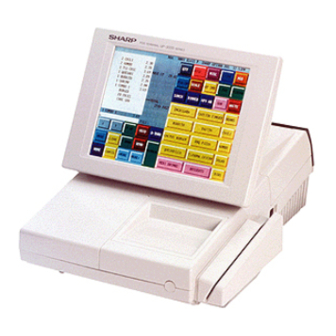
POS TERMINAL
UP-3300
MODEL
(For "V" version)
This document has been published to be used
for after sales service only.
The contents are subject to change without notice.
Advertisement
Chapters
Table of Contents

Related Manuals for Sharp UP-3300


Summary of Contents for Sharp UP-3300
- Page 1 CODE: 00ZUP3300VSME POS TERMINAL UP-3300 MODEL (For "V" version) CONTENTS CHAPTER 1. SPECIFICATIONS ........1-1 CHAPTER 2.
- Page 2 BATTERY DISPOSAL Contains Nickel Metal Hydride Battery. Must be Disposed of Properly. Contact Local Environmental Officials for Disposal Instructions.
- Page 3 640 (W) × 480 (H) mm Full dot Dot format 0.09 × RGB(W) × 0.31 mm Dot size Dot space 0.02 mm ∗ Note that the application software for the UP-3300 uses 16 colors. 1 – 1...
- Page 4 Screen example (REG mode) Time Mode caption NOTE Once the internal clock unit is started at the correct time, it continues to run as long as the battery pack is charged and will also update the date properly. Touch-panel keyboard Numeric entry: An entered figure appears at the cursor position.
- Page 5 Display example 2 (PGM mode) Clerk name Time Mode caption Clerk code Double-size character mode indicator (W): Window: Appears when the double-size character mode is In the PGM mode, programmable selected during text programming. items are listed. Screen save mode To save electrical power or the display’s life, your POS terminal is provided with the screen save function.
- Page 6 • • Condiment1 keyboard Function menu 12 (MGR) keyboard This keyboard appears when you touch the MENU key in a condi- This keyboard appears when you touch the key. ment PLU entry. (FNC.12) START. FISH MEAT DESS. HOME MENUE MENUE MENUE MENUE HOME...
- Page 7 • • Function menu 7 (X/Z COMMAND) keyboard Character keyboard This keyboard appears when you touch the X/Z COMMAND key This keyboard is used when you need to enter text data during on the X/Z mode keyboard. PGM2 mode entries. AUTO18 AUTO19 CANCEL...
- Page 8 Function keys list (default keyboard and labels) Caption (default) Function CR1 thru CR8 Used to enter the credit sale (credit 1 thru Caption (default) Function HOME Used to return to HOME keyboard. EXCHANGE1 to Used to creates a subtotal in foreign CANCEL Used to cancel your current operation or EXCHANGE9...
- Page 9 The standard POS terminal has been shipped with the real clerk key system being programmed. If you want to change the clerk identifica- tion system, contact your authorized SHARP dealer. Real clerk keys (1, 2, 3, 4, 5, and 6) These keys serve to identify clerks.
- Page 10 2 – 1...
- Page 11 2. Sales Options CLASSIFICATION COMPONENT NAME MODEL NAME REMARK Printer External R/J printer ER-01PU Via RS-232 I/F Remote printer ER-03RP Via SRN I/F ER04RP Built-in printer UP-T80BP Via RS-232 (TTL level) Display Remote display (Pole type) UP-P16DP 11-Dig. 7-Seg.+16-Dig. Dot Drawer Remote drawer ER-03DW...
- Page 12 NAME PARTS CODE DESCRIPTION LKGIM1004BH29 1 hole clerk key Key No. 29 The key No.1 to No.6 ore supplied together with UP- LKGIM1004BH30 Key No. 30 5700. LKGIM1004BH31 Key No. 31 LKGIM1004BH32 Key No. 32 LKGIM1004BH33 Key No. 33 LKGIM1004BH34 Key No.
- Page 13 NAME PARTS CODE DESCRIPTION 1 hole clerk key LKGIM1004BH89 Key No. 89 The key No.1 to No.6 ore supplied together with UP- LKGIM1004BH90 Key No. 90 5700. LKGIM1004BH91 Key No. 91 LKGIM1004BH92 Key No. 92 LKGIM1004BH93 Key No. 93 LKGIM1004BH94 Key No.
- Page 14 Test pins : Used to check the bus signals. 5-2. MCR test card: UKOG-6718RCZZ Bus connector : Used to check the bus signals. • Used when executing the diagnostics of the UP-E12MR2. • External view Connected to the UP-3300 Mother PWB. 2 – 5...
- Page 15 UP-3300 ........
- Page 16 5) Correction points are displayed * If the power supply is turned off during correction, the following messages are displayed and all the steps are started over again. The correction points are displayed. All of the nine correcting points are displayed as follows using the Calibration failed.
- Page 17 393, 2048 2080, 2048 3767, 2048 3300 series. The "UTL33.EXE" is a program which runs on the PC DOS prompt screen, it is connected to the UP-3300 through IR. It has 393, 3697 2080, 3697 3767, 3697 the following functions: (1) UP-3300 IPL operation; (2) LOGO data Touch panel coordinates rewrite for built-in printer UP- T80BP;...
- Page 18 Turn ON the power. Starting of "IPL Mode". UP-3300 shows "IPL from IR" IPL from IR Connect P.C. and UP-3300 via IR. (Fig 1) Execute "UTL33.EXE" on P.C. Operation: >UTL33 3300_1.ROM 3300_2.ROM ("3300_1.ROM" and "3300_2.ROM" are file name of S-type ROM object.)
- Page 19 Procedure on UP-3300 side Install "UTL33.EXE" on the P.C. Enter the SRV mode. Then turn OFF the power or UP-3300. While pressing the On-Line key, tum ON the power of UP-3300. Keep pressing the On-Line key, and then press the Feed key also.
- Page 20 2: UP-T80BP LOGO STAMP "UTL33.EXE" is a utility program on P.C. - a program that sends the application program data of UP-3300, the image data of the Logo 3: UP-T80BP IPL stamp of UP-T80BP or the application program data of UP-T80BP in Normally, UTL33.EXE takes the suitable function automatically.
- Page 21 5. Conditions for soldering circuit parts To solder the following parts manually, follow the conditions described below. PARTS NAME PARTS CODE LOCATION CONDITIONS FOR SOLDERING RCRMZ7002RCZZ Ceramic oscillator MAIN PWB: X1 (8M) 270°/3sec. RCRMZ7004RCZZ MAIN PWB: X2 (7.37M) 270°/3sec. • How to Connect or Disconnect FFC 6.
- Page 22 PARTS NAME PARTS CODE LOCATION QCNCW7217RC3J TOUCH CONNECTOR PWB: CN1 • How to Insert FFC (1) Open the slider to unlock position Open the slider upwards up to an angle of 60 degrees. If the slider does not fully open, the FFC can not be smoothly inserted. (2) Insert the FFC Insert the FFC firmly until the FFC hits the bottom of the connector’s insulator.
- Page 23 SRV mode DISPLAY: [SRV mode screen] In the UP-3300, the following reset switch (location No: S1) is used to switch to the service (SRV) mode and to reset. NOTE: Do not turn on the MRS switch with the main power supply switch turned ON;...
- Page 24 8) MASTER RESET-1 is started. CHAPTER 5. MASTER RESET DISPLAY: (All Memory Clear) There are three possible methods to perform a master reset. MASTER RESET 1. MRS-1 (Master resetting 1): Clear the entire memory and resumes initial 9) After completion of the master reset, the buzzer sounds three values.
- Page 25 6) The master reset menu window is displayed as shown below. 10) After completion of the master reset, the buzzer sounds three times and the following SRV mode display is shown. DISPLAY: DISPLAY: [SRV mode screen] Please select MASTER RESET MASTER RESET 2 Touch the [MASTER RESET 2] key.
-
Page 26: Table Of Contents
1) Remote Display Check ..........6-7 2 Set the CKDC reset switch to RESET position. 3-9. SHARP Retail Network Diagnostics........ 6-7 3 Turn on the power. 1) SRN Self Check............6-7 4 While touching the touch panel, place the CKDC RESET SWITCH 2) SRN Flag Send Check.......... -
Page 27: Ram Diagnostics
Check point address = 700000H, 700001H UP-3300 Diagnostics V1.0A 700002H, 700004H 700008H, 700010H Product & Test Diag IrDA Diag 700020H, 700040H RAM Diag Drawer Diag 700080H, 700100H 700200H, 700400H ROM & SSP Diag Remote Display Diag 700800H, 701000H Clock & Clerk Diag... -
Page 28: Rom & Ssp Diagnostics
The format of data (ASCII) to be stored is as fol- lows: SSP Check D1FFE0H ∼ D1FFEFH: Model name code (example: UP-3300. Display is made up to 00H of data.) D1FFF0H ∼ D1FFF9H: 27801R****(****=PROGRAM VERSION) D1FFFAH ∼ D1FFFBH: BLOCK NO. ("20" ∼ "2F") D1FFFCH: TERMINATOR ("=") -
Page 29: Timer & Clerk Switch Diagnostics
Check the time updated and indicated. When setting channels of RS232, do not set two or more ports to one channel. In the UP-3300, max. two units of ER-A7RS can be Timer Diagnostics installed. In each PWB, do not set two or more ports to the same DATE &... -
Page 30: Ch1 Check
• ER-A7RS CON3 Data transfer check The loop back data (256 bytes) of 00H ∼ 0FFH are used for S1-1 S1-2 S1-3 CHANNEL data transfer check. The baud rate is set to 38400BPS. Invalid • Timer check (RS232 on board timer) CHANNEL 1: Do not set this Before performing the check, set the timer to TCVDT start and (Reserved for... -
Page 31: Ch6 Check
The check procedure, the display, and the terminating procedure are the same as CH1 Check. 3-7. Liquid Crystal Display Diagnostics The UP-3300 LCD display is checked. The test program displays the patterns in the following sequence. Every time when the Touch panel is pressed, the next pattern is displayed. -
Page 32: Remote Display Diagnostics
DMA sent data and received data are different. b4 The number of data received in DMA is abnormal. 3-9. SHARP Retail Network Diagnostics b3 The number of data transmitted in DMA is abnormal. The SRN test is performed. -
Page 33: Srn Flag Send Check
The error status from the controller to the host is as shown in 4) Data Transmission Check the table below. Data transmission is checked in an actually composed system. The system is composed of one master machine and max. 15 satellite b7 Not used. -
Page 34: Irda & Ask Diagnostics
• The master machine receives the data, and checks the se- • UP-3300 as checker quence No. and 256byte AAH data. In case of an error, the The following menu is displayed. Press the touch key for the opera- master machine displays an error code and terminates the tion you want to execute to execute individual Diag programs. -
Page 35: Irda & Ask Check
2 Display 1) IrDA & ASK Check IR communication is checked between the UP-3300 sending unit and Data Transmission Check (Send MODE) the receiving unit. COUNTER : **** (The RING COUNTER (0~9999) is displayed.) 1 Check content • Data transmission is made from the machine to be checked in 3 Terminating procedure ASK format. -
Page 36: Drawer 1 Check
1) Drawer 1 Check 2) Printer Print Check 1 Check content 1 Check The solenoid of drawer 1 is turned on, and the drawer open Send the signal to generate a receipt (by DIAG COMMAND) to sensor value is sensed at every 100ms, and the state is dis- the UP-T80BP. - Page 37 CHAPTER 7. CIRCUIT DESCRIPTION 1. Hardware block diagram Drawer x 2 DRIVER +24V H8/510 DRIVER +24V FLASH MPCA8 RS232 x 2 DRIVER/ PSEUDO RECEIVER SRAM OPC2 EXT.SLOT (80pin x 2) RAMCN (72pin) PRINTER VRAM TOUCH PANEL CONTROLLER (DRAM 512K) CKDC9 CONTROLLER MN89303A BRIGHTNESS...
- Page 38 2. Description of main LSI’s 2-1. CPU (HD6415108FX) 1) Pin description AVSS 7 – 2...
- Page 39 2) Block diagram P27/A23 P26/A22 Data bus Port 1 P25/A21 P24/A20 P23/A19 P22/A18 P21/A17 P20/A16 EXTAL XTAL Clock Watch oscillator dog timer H8/500 CPU STBY Interruption controller 16bit free running Refresh controller timer x 2ch RFSH BREQ BACK Wait state 8bit timer controller WAIT...
- Page 40 Data bus /STOP System reset output signal Data bus /IPLON0 From IPL SW of ER-A7RS Data bus /IPLON1 From IPL SW of UP-3300 Data bus Data bus NORDY Flash Memory ready ("H" active) Data bus FVPON Flash Memory write protect ("L"...
- Page 41 2-2. G.A.(MPCA8) 1) Pin configuration EXINT0Z EXINT1Z PCUTZ EXINT2Z FCUTZ EXINT3Z WROZ STAMPZ RDOZ VIOZ RA15 VMEMZ RA16 SWAPZ RESZ RA17 FROS1Z RA18 FROMLZ EXWAITZ POFF WAITZ INT1Z MCR2Z HTS1 IPLON SCK1 DAX2 STH1 DAX1 MCRINT RCRXZ VWAITZ IRRXZ MCRINTZ UATXZ VRESC UARXZ...
- Page 42 2) Block diagram M P C A 8 A23-A0 IPLONZ VMEMZ DROS1Z SSP COMPARISON RASPN1 REGISTER SSPRQZ DECODE RASPN1E RASPN12Z RASPN2 RASPN2E IRTX IRRXZ RCRXZ D0-D7 BUFFER UASCK CONTROL UARXZ UATXZ DAX1 RDOZ DAX2 READ WROZ WRITE PHAI CONTROL TXDI RESETZ SCKI RESZ...
- Page 43 3) Pin description Name Description Name Description INT3Z INTERRUPT INPUT (/TPTRDY) RXDI SERIAL OUT FOR CPU PCUTZ TXDI SERIAL IN FROM CPU FCUTZ SCKI SERIAL CLOCK FROM CPU IRQ0Z INTERRUPT SIGNAL FOR CPU STAMPZ ADDRESS BUS VIOZ ADDRESS BUS VMEMZ VRAM DEOCDE ADDRESS BUS SWAPZ...
- Page 44 Name Description Name Description UARXZ IR DATA FOR CPU 148 SLMTS UATXZ IR DATA FROM CPU 149 RCP1 CLOCK PULSE FROM MCR TRACK1 100 VDD – 150 HTS2 SERIAL OUT (OPTION CKDC INTERFACE) 101 GND – 151 SCK2 SERIAL CLOCK (OPTION CKDC 102 IRRXZ IR IN FROM IR UNIT INTERFACE)
- Page 45 2-3. OPC2 1) Pin configuration SL00 TRNDTB SL01 /CSB SL02 SL10 SYCBKA SL11 TRNEMPA SL12 RCVRDYA SL20 TRNRDYA SL21 /DSRA SL22 /CTSA SL30 RCVDTA SL31 /RTSA SL32 /DTRA /CD0 TRNDTA BRK0 /CSA TRNEMP0 UTST RCVRDY0 DBTST TRNRDY0 RCVCLK /CTS0 TRNCLK RCVDT0 /CI0 /RTS0...
- Page 46 OPC1 DATA BUS OPC1~USART BAUD RATE GENERATOR BAUD RATE GENERATOR USART USART USART USART USART Common input 3) Pin description Name UP-3300 Description Name UP-3300 Description SL00 RS-232/UNIT0 24 /CS0 /CS1 RS-232 chip select channel select signal SL01 25 /CD1...
- Page 47 Name UP-3300 Description Name UP-3300 Description 40 RCVDT2 RCVDT3 RS-232 reception to 90 DB1 DATA BUS (USART) send signal 91 DB2 DATA BUS (USART) 41 /CI2 92 DB3 DATA BUS (USART) 42 /CS2 /CS3 RS-232 chip select 93 GND signal...
- Page 48 • The Z80 microprocessors and associated family of peripherals can Name UP-3300 Description be linked by a vectored interrupt system. This system can be daisy-chained to allow implementation of a priority interrupt 131 /CSC /CS3 USART_C chip select scheme. 132 TRNDTC...
- Page 49 3) General description Signal Symbol In/Out Function name The CPUs are fourth-generation enhanced microprocessors with ex- ceptional computational power. They offer higher system throughput S RDS Rread signal and more efficient memory utilization than comparable second- and S WRS Write signal third-generation microprocessors.
- Page 50 During operation, the individual counter channel counts down from the preset time constant value. In counter mode operation the counter CLK/TRG0 decrements on each of the CLK/TRG input pulses until zero count is ZC/TO0 reached. Each decrement is synchronized by the system clock. For counts greater than 256, more than one counter can be cascaded.
- Page 51 3) Pin configuration Signal Symbol In/Out Function name Signal Symbol In/Out Function — name S A1 Channelselect signal READY READY Ready signal 36 CLK/TRG3 S TM1 External clock / timer signal HLDAK HLDAK Hold acknowledge signal 37 CLK/TRG2 S TM0 External clock / timer signal ASTB S ASTB...
- Page 52 The MB62H149 is a semi-custom LSI chip for the peripheral circuits (b) CPU and DMAC wait signal control unit in the SRN (SHARP Retail Network), its main function is to communi- Clocks into the CPU (Z-80), SUB CPU and its peripheral LSI, cate data with the host CPU and control the peripheral circuits and DMAC and CTC are operated respectively on 4 MHz.
- Page 53 3) Terminal Name and Description (MB62H149) Terminal Host/ Description name IO/WR I/O write 23.9 ± 0. 6 IO/RD I/O read Address enable from DMAC Address strobe from DMAC Terminal count DAK23 DMA acknowledge 2+3 DRQRS DMA request read to sub DRQWS DMA request write to sub Host...
- Page 54 2-8. VGA controller (MN89303A) 1) Pin Configuration /SBEH /IOWR /IORD /SMEMW /SMEMR SA19 SA18 LOGICON SA17 LCDON SA16 BACKON SA15 SA14 SA13 SA12 SA11 SA10 /BIOSEN /REFRESH 2) Block diagram Gray scale RAM table engine Hardware UD[7:0] cursor LD[7:0] BACKON LCD panel LCDON controller...
- Page 55 3) Pin configuration Signal Signal Symbol Function Symbol Function name name 25.175MHz DCLK Out Data shift clock DISP DISP Out Display enable /SBEH /SBEH System byte high enable Out Line pulse /IOWR /IOWR I/O write OUt Frame pulse /IORD /IORD I/O read Out Upper data /SMEMW...
- Page 56 — 2-9. CKDC9 (HD404728A91FS) Dot display controller chip select — 1) General description The CKDC7 is a 4-bit microcomputer developed for the UP-3300 and VCKDC — provides functions to control the real-time clock, keys, and displays. Clock signal The basic functions of the CKDC7 are shown below.
- Page 57 2-10. ISP2032 Name Function This IC has been developed specially for UP-3300 to achieve VGA CHIP and PSRAM interfaces. RASPN2E EXTENDED PSRAM2 DECODE (FROM MPCA) Pin descriotion 800000H ∼ 9FFFFFH RASPN2 EXTENDED PSRAM2 DECODE Name Function (FROM MPCA) 800000H ∼ 9FFFFFH...
- Page 58 Fig. 4 3-4. ROM space 3-5. VRAM & RAM space Fig.5 shows the ROM space. The UP-3300 uses 2MB of NOR-type The VRAM is the display memory of the LCD. flash memory instead of conventional ROM, so that the ROS1 from...
- Page 59 3-6. Extended I/O area The addresses from F00000h to FFFFFFh are called an extended I/O area. The UP-3300 uses the following addresses as the break ad- dress register (BAR) for SSP. FFFF00h ∼ FFFFFFh • 4. LCD display The main display is a 640 × 480 dot liquid crystal display.
- Page 60 The figure below shows a typical pseudo SRAM interface in the up- 8. SSP control 3300. ISP2032 The UP-3300 uses flash memory in the place of EPROM, so it is Odd side PSRAM /OWR /LWR possible to rewrite the contents of the flash memory in changing the /HWR program.
- Page 61 WAITZ is the wait re- Extension RAM connector terminals quest signal from the VGA controller. Signal Signal Signal Name Name Name 11. CKDC9 — The UP-3300 performs the following controls, using CKDC9. — • Customer display — — • Clock — — •...
- Page 62 MRS, SRV is different from that of conventional cash • P33=1: Any of the drawers is open. registers. in the UP-3300, MRS, SRV resetting is selected and executed by the 15. IR communication key which has bee depressed when the CKDC reset is released to start the system.
- Page 63 RCVRDY2 CLS1, 20. 1-HOLE CLERK CLS2 SYNC On the UP-3300, 1-hole clerk key with up to 8 bits can be used. The 1-hole clerk switch is controlled through the CKDC9 on the main Signal description board. RCP1 TRACK 1 CLOCK PULSE...
- Page 64 8 – 1...
- Page 65 8 – 2...
- Page 66 8 – 3...
- Page 67 8 – 4...
- Page 68 8 – 5...
- Page 69 8 – 6...
- Page 70 8 – 7...
- Page 71 8 – 8...
- Page 72 8 – 9...
- Page 73 8 – 10...
- Page 74 8 – 11...
- Page 75 8 – 12...
- Page 76 8 – 13...
- Page 77 8 – 14...
- Page 78 8 – 15...
- Page 79 8 – 16...
- Page 80 8 – 17...
- Page 81 8 – 18...
- Page 82 8 – 19...
- Page 83 8 – 20...
- Page 84 8 – 21...
- Page 85 8 – 22...
- Page 86 8 – 23...
- Page 87 9 – 1...
- Page 88 9 – 2...
- Page 89 2. IR PWB 3. LCD PWB [A Side] [B Side] 4. INVERTER PWB [A Side] [B Side] 9 – 3...
- Page 90 9 – 4...
- Page 91 UP-3300V UP -3300V PARTS GUIDE UP-3300 MODEL (for KA,KB,TQ,TS) CONTENTS Top cabinet etc. N/F PWB unit Bottom cabinet etc. Invertor PWB unit Packing material & Accessories IR PWB unit Main PWB unit LCD PWB unit Mother PWB unit Service route options & Service tools...
-
Page 92: Top Cabinet Etc
UP-3300V UP -3300V 1 Top cabinet etc. PRICE PART PARTS CODE DESCRIPTION RANK MARK RANK 1 G S T N - 2 0 0 5 B H Z Z Tilt stand 2 J K N B Z 2 4 1 1 B H Z Z Tilt knob 3 M S P R P 2 3 7 2 B H Z Z Tilt spring... - Page 93 UP -3300V UP-3300V 1 Top cabinet etc. 39 40 PSP00132 – 2 –...
-
Page 94: Bottom Cabinet Etc
UP-3300V UP -3300V 2 Bottom cabinet etc. PRICE PART PARTS CODE DESCRIPTION RANK MARK RANK 1 L X - B Z 6 7 8 2 B H Z Z Screw (3×8KS) 7 X E B S D 3 0 P 0 8 0 0 0 Screw (M3×8) 8 L A N G T 7 6 3 8 B H Z Z Option angle 2... - Page 95 UP -3300V UP-3300V 2 Bottom cabinet etc. PSP00133 – 4 –...
-
Page 96: Packing Material & Accessories
UP-3300V UP -3300V 3 Packing material & Accessories PRICE PART PARTS CODE DESCRIPTION RANK MARK RANK 1 S P A K C 3 0 3 3 B H Z Z Packing case 2 S P A K A 8 4 5 4 B H Z Z Packing add R 3 S S A K H 0 0 0 3 D H Z Z Vinyl bag (640×560mm) -
Page 97: Main Pwb Unit
UP -3300V UP-3300V 4 Main PWB unit PRICE PART PARTS CODE DESCRIPTION RANK MARK RANK 1 Q S O C Z 1 0 1 2 A C 7 B Socket (MM20-72B2-1-T24) [CN9] 2 V C K Y T V 1 H B 1 0 2 K Capacitor (50WV 1000PF) [C1,2,264] V C K Y T V 1 H F 1 0 4 Z... - Page 98 UP-3300V UP -3300V 4 Main PWB unit PRICE PART PARTS CODE DESCRIPTION RANK MARK RANK V C C C T V 1 H H 1 0 1 J Capacitor (50WV 100PF) [C233,234,236,237,240,241,242] V C C C T V 1 H H 1 0 1 J Capacitor (50WV 100PF) [C247,248,249,250,251,252,256,31,33] V C C C T V 1 H H 1 0 1 J...
- Page 99 UP -3300V UP-3300V 4 Main PWB unit PRICE PART PARTS CODE DESCRIPTION RANK MARK RANK Resister (1/10W 14KΩ ±1%) 115 V R S - T S 2 A D 1 4 3 F [R235A] Resistor (1/10W 22KΩ ±5%) 116 V R S - T S 2 A D 2 2 3 J [R239] Resistor (1/10W 8.0KΩ...
-
Page 100: Mother Pwb Unit
UP-3300V UP -3300V 4 Main PWB unit PRICE PART PARTS CODE DESCRIPTION RANK MARK RANK 197 V H I K I A 7 0 4 5 F - 1 IC (KIA7045) [IC54] 198 Q C N W - 3 0 2 2 B H Z Z GND wire Resistor (1/10W 4.7KΩ... -
Page 101: Ir Pwb Unit
UP -3300V UP-3300V 8 Invertor PWB unit PRICE PART PARTS CODE DESCRIPTION RANK MARK RANK 1 Q C N C M 2 6 5 6 R C 0 C Connector (BHR-03VS-1) [CN501A] 2 R C - C Z 2 2 0 1 R C 0 F Capacitor (22pF/3.15KV) [C504A] 3 R C I L C 6 6 6 7 B H Z Z... - Page 102 UP-3300V UP -3300V 11 Service route options & Service tools PRICE PART PARTS CODE DESCRIPTION RANK MARK RANK 22 L K G I M 1 0 0 4 B H 1 8 Clerk key(18) (2pcs/1set,with key ring) 23 L K G I M 1 0 0 4 B H 1 9 Clerk key(19) (2pcs/1set,with key ring) 24 L K G I M 1 0 0 4 B H 2 0 Clerk key(20) (2pcs/1set,with key ring)
- Page 103 UP -3300V UP-3300V 11 Service route options & Service tools PRICE PART PARTS CODE DESCRIPTION RANK MARK RANK 102 L K G I M 1 0 0 4 B H 9 8 Clerk key(98) (2pcs/1set,with key ring) 103 L K G I M 1 0 0 4 B H 9 9 Clerk key(99) (2pcs/1set,with key ring) 104 L K G I M 1 0 0 4 B H 0 0 Clerk key(100) (2pcs/1set,with key ring)
- Page 104 UP-3300V UP -3300V Index PRICE PART PARTS CODE RANK MARK RANK LKGIM1004BH18 11- 22 PRICE PART PARTS CODE LKGIM1004BH19 RANK MARK RANK 11- 23 LKGIM1004BH20 11- 24 CKOG-6724BHZZ LKGIM1004BH21 11- 25 CPWBF7573BH02 LKGIM1004BH22 2- 22 11- 26 " LKGIM1004BH23 7-901 11- 27 CPWBF7573BH03 LKGIM1004BH24...
- Page 105 UP -3300V UP-3300V PRICE PART PRICE PART PARTS CODE PARTS CODE RANK MARK RANK RANK MARK RANK LKGIM1004BH99 QCNW-2975BHZZ 11-103 2- 32 LKGIM1004BHA0 QCNW-2976BHZZ 11-114 1- 16 LKGIM1004BHA1 QCNW-2982BHZZ 11-105 LKGIM1004BHA2 QCNW-2989BHZZ 11-106 4-157 LKGIM1004BHA3 QCNW-2990BHZZ 11-107 4-158 LKGIM1004BHA4 QCNW-2992BHZZ 11-108 2- 16 LKGIM1004BHA5...
- Page 106 UP-3300V UP -3300V PRICE PART PRICE PART PARTS CODE PARTS CODE RANK MARK RANK RANK MARK RANK SPAKC3033BHZZ VHD1SS353//-1 6- 11 SSAKA5004CCZZ VHDCP301///-1 4-179 SSAKH0003DHZZ VHDSFPB54//-1 4- 12 SSAKH3015CCZZ " 4- 75 SSAKH4231CCZZ " 3- 10 8- 13 VHDSFPL52V/-1 4- 11 TCADH6788BHZA VHEMTZ5.1A/-1 3- 11...
- Page 107 UP -3300V UP-3300V PRICE PART PRICE PART PARTS CODE PARTS CODE RANK MARK RANK RANK MARK RANK VRS-TS2AD105J 4- 47 " 4-104 VRS-TS2AD112J 4-119 VRS-TS2AD122F 4-109 VRS-TS2AD122J 4- 98 VRS-TS2AD123J 4- 96 VRS-TS2AD133F VRS-TS2AD143F 4-115 VRS-TS2AD152G 4- 94 VRS-TS2AD152J 4-120 VRS-TS2AD153G 4- 50 VRS-TS2AD153J...
- Page 108 COPYRIGHT 1999 BY SHARP CORPORATION All rights reserved. Printed in Japan. No part of this publication may be reproduced, stored in a retrieval system, or transmitted, in any form or by any means, electronic, mechanical, photocopying, recording, or otherwise, without prior written permission of the publisher.