
Related Manuals for Lanner LVC-2000


Summary of Contents for Lanner LVC-2000
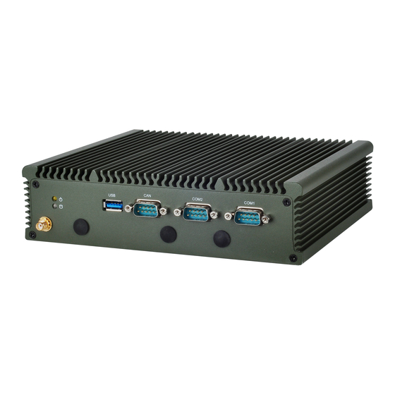
- Page 1 In-Vehicle Computing Hardware Platforms for mobile applications LVC-2000 V1.3 >> User Manual Release Date: 2022/03/03...
- Page 2 Resource Website installed and used in accordance with the instruction manual, may cause harmful interference to radio Lanner website www.lannerinc.com communications. Operation of this equipment in a residential area is likely to cause harmful interference in Download Center lannerinc.com/support/download-center...
- Page 3 Mechanical compliance Revision History Vibration: 2014/09/14 Preliminary General Vibration (operating): Refer to MIL-STD-810G, • 2014/12/10 Official release Method 514.6, Procedure I (Transportation), Category 2015/11/19 Revised COM pinouts 4 – Common carrier (US highway truck vibration 2016/06/01 Modified MCU and SW exposure) pinouts General Vibration (non-operating): Refer to MIL-STD-...
-
Page 4: Table Of Contents
Connecting Power Chapter 4: The Flow Chart Appendix A: Using the Ignition System Manager (ISM) Appendix B: Digital Input/Output Appendix C: Accessing the GPS Data from the LVC-2000 Appendix D: Programming System Watchdog Timer Appendix E : Terms and Conditions... -
Page 5: Chapter 1: Introduction
Memory type AMI SPI Flash BIOS BIOS LVC-2000 is a fanless in-vehicle computer with MIL- STD-810G certified shock and vibration resistance. 1x mSATA with SATA 3.0Gbps, mSATA/ Storage 1x SATA 2.5” drive bay for HDD/SSD Built with onboard Intel®... -
Page 6: Package Contents
Package Contents Fanless system. Heat dissipate from Thermal Solution aluminum enclosure Your package contains the following items: Suspending Kit or wall mounting-1 LVC-2000 Fanless Embedded System with rubber Mounting stands: Terminal Block Connectors: • CE, FCC Class A, E13, RoHS... -
Page 7: Chapter 2: System Components
Chapter 2: System Components Mechanical Drawings Mechanical dimensions of the LVC-2000 with the system itself Unit: mm... - Page 8 Mechanical dimensions of the LVC-2000 with anti-vibration kit Unit: mm...
- Page 9 Mechanical dimensions of the LVC-2000 with wall-mounting kit Unit: mm...
-
Page 10: Block Diagram: The Mainboard
Block Diagram: The MainBoard The block diagram depicts the relationships among the interfaces and modules on the motherboard. -
Page 11: Front Components
Front Components Component Description Remarks F1 GPS Antenna Reserved for GPS antenna F2 LED Indicator HDD/SSD LED • Blinking: means data access activities • Off: means no data access activities or no hard disk present Power LED • On: The computer is on. •... -
Page 12: Rear Components
Rear Components Component Description Remarks R1 Multiple-I/O Connector A 20-pin male connector for the following functions: • 4x DI (5V or 12V TTL selectable) • 4x DO (12V TTL , Max. 100mA) • 2x MCU DI • 2x Relay • 1x 12V Output @Max. -
Page 13: Internal Connectors And Jumpers
Internal Connectors and Jumpers The following picture highlights the location of internal connectors and jumpers. Refer to the table 3.2 Connector List for more details. USBF1 MSATA1 JMCU1 JSPI1 JCMOS1 MPCIE2 SIM1 MPCIE1 SATA1 JRI1 JKBMS1 JLPC1 SATAPWR1 JRI2... -
Page 14: Internal Connectors And Jumpers (Backside)
Internal Connectors and Jumpers (backside) The following picture highlights the location of internal connectors and jumpers on the backside of the board. Refer to the table 3.2 Connector List for more details. -
Page 15: Connectors And Jumpers List
Connectors and Jumpers List The tables below list the function of each of the board jumpers and connectors by labels shown in the above section. The next section in this chapter gives pin definitions and instructions on setting jumpers. Table 3.1 Connector List for External Connectors Labels Function CAN1... -
Page 16: Jumper Settings
Jumper Settings Connectors JCMOS1 (Clean CMOS): VGA (VGA1) This jumper is used to erase data in CMOS. To clear CMOS, 5 4 3 2 1 first turn off your system and unplug power source. Then, by placing the cap on pin 2 and 3 (short pin 2-3), this jumper can erase the system settings stored in CMOS 15 14 13 12 11 memory. - Page 17 mSATA (MSATA1) USB3.0 (USB2) It complies with SATA 3.0Gbps interface Description Description V5S_USB2 USB3_SSRXN USBDN2 USB3_SSRXP Description Description USBDP2 SMB_CLK USB_SSTXP V3P3S mSATATXN USB_SSTXN SMB_DAT mSATATXP LAN (LAN1) V3P3S V3P3S Description Description MDI_P0_LAN1 MDI_N2_LAN1 MDI_N0_LAN1 MDI_P3_LAN1 MDI_P1_LAN1 MDI_N3_LAN1 MDI_N1_LAN1 LNK100_LAN1 LNK1000_LAN1 V3P3A mSATARXP...
- Page 18 MPCIE1: Mini-PCIe Connector with one SIM Card COM1&2 Reader(SIM1). It supports both Wi-Fi and 3G module. 1 2 3 4 5 6 7 8 9 Signal Signal RS-232 RS-422 RS-485 PCIE_WAKE_N VCC3P3_PS TXD- DATA- V1P5_MPCIE TXD+ DATA+ E_CLKREQ- UIM_PWR RXD+ UIM_DATA RXD- PCIE_CKN3...
- Page 19 SPI (JSPI1) Maximum input/output current for each port is 100mA For all Input/ Voltage Logic Register DI: <0.8V output pins: DO: <0.4V DI: 10 ~ 12V High Description SPI_HOLD DO:12V SPI_CS0 The default BIOS value is 0 for DI and 1 for DO VCC3 Pin3 and pin4 can be used for DI wake-up SPI_MISO...
- Page 20 CAN Bus Connector (CAN1) 1 2 3 4 5 6 7 8 9 Pin No. Pin Name J1850-/J1708- GND_CAN CAN_H/J1939+ K_LINE CAN_L/J1939- J1850-/J1708- J1850+/J1708+ J1850+/J1708+ BAT_12V_24V AUDIOIN1: Line-out and Mic-in Connector Pin No. Pin Name MIC_IN_L MIC_IN_R GND_AUO GND_AUO FRONT_OUT_L FRONT_OUT_R...
-
Page 21: Chapter 3: Hardware Setup
Portions of the power supply and some internal circuitry might remain active until power is removed. Unpower the LVC-2000 and remove the power cord. Remove 4 threaded screws from the bottom to take off the bottom cover. -
Page 22: Msata Card Installation
mSATA Card Installation 3G SIM Card Installation Align the mSATA card’s key with the Mini-PCIe slot Unlock the SIM card reader. notch. Place the SIM card on the SIM card reader. Notice the Insert the wireless module into the connector angled corner to align the SIM card properly. -
Page 23: Connecting Power
Connecting Power Connect the LVC-2000 to a +9V ~ +36V vehicle battery. The DC power-in connector comes with a 3-pin terminal block for its Phoenix contact. This power socket can only accept the power supply with the right pin contact so be cautious when inserting power to the system. -
Page 24: Chapter 4: The Flow Chart
Chapter 4: The Flow Chart The flow chart section contains all flow chart used in the system. The flow chart describes the system’s behavior on powering on and off the system via power ignition control or on/off switch when the appropriate timer control parameters are set. -
Page 25: Appendix A: Using The Ignition System Manager (Ism)
COM5 features that the Power Ignition Module provides. For sample ISM code, see ISM folder under LVC-2000 Utility on the Driver and Manual CD. Running the Program Just double click the ISM.exe to launch the ISM. -
Page 26: Appendix B: Digital Input/Output
The Digitanl I/O on the rear panel is designed to provide the input and output operations for the system. For sample DIO code, see SuperIO folder under LVC-2000 Utility on the Driver and Manual CD. Make sure that you have installed the Lanner GPIO driver as instructed below. - Page 27 Choose to select the hardware Manually Click HaveDisk to locate the L_IO.inf file Choose Show all device and click Next. Select the L_IO.inf Select OK to confirm with the installation Click HaveDisk to locate the L_IO.inf file...
- Page 28 Select the Lanner IO driver and click Next. To verify the GPIO driver installation, do the following steps: Right-click on the My Computer icon, and then select Properties form the menu. Click the Hardware tab, then click the Device Manager button.
- Page 29 A sample DIO program in C: ioaccess.c: IO access code for Lanner Platfomr Digital IO program #include <time.h> ********************************************************* #include <stdint.h> **********************/ #include <fcntl.h> #include <errno.h> #include <string.h> #define delay(x) usleep(x) #include “../include/config.h” #endif #ifdef DJGPP #ifdef MODULE /* standard include file */ #include <linux/kernel.h>...
- Page 30 #include <machine/bus.h> outportb(INDEX_PORT, 0xAA); #include <machine/resource.h> return; #endif #endif unsigned char read_SIO_reg(int LDN, int reg) /* local include file */ outportb(INDEX_PORT, 0x07); //LDN register #include “../include/ioaccess.h” delay(5); outportb(DATA_PORT, LDN); #if (defined(MODULE) || defined(DIRECT_IO_ACCESS) || delay(5); defined(KLD_MODULE)) outportb(INDEX_PORT, reg); delay(5); return(inportb(DATA_PORT)); *------------------------------------------------------------------------- ----- * LEB-5000 Version V1.0...
- Page 31 exit_SIO_config(); return; void dio_set_output(unsigned char out_value) enter_SIO_config(); write_SIO_reg(0x6, 0xf1, ((read_SIO_reg(0x6, 0xf1)& 0xF0)|out_value)); exit_SIO_config(); return; unsigned int dio_get_input(void) unsigned int tmp=0x00; enter_SIO_config(); tmp=read_SIO_reg(0x6, 0xA2)& 0x0f; exit_SIO_config(); return tmp; //====================================== ======================================== ================= #endif...
-
Page 32: Appendix C: Accessing The Gps Data From The Lvc-2000
SBAS: WAAS, EGNOS, from the LVC-2000 MSAS Time-To-First-Fix (All Cold Start: 26 s The LVC-2000 employs an onbard u-blox NEO-7N GPS satellites at -130 dBm) Warm Start: 26 s module for vehicle tracking and navigation system. You Hot Start: 1 s could read the GPS data through the RS-232 serial port. - Page 33 Specify the following communication parameters: Bits per Second: 9600 Data Bits: 8 Parity: None Stop Bit: 1 9600 Flow Control: None The hyper terminal should display GPS data:...
-
Page 34: Appendix D: Programming System Watchdog Timer
“ F81865_test AlarmLED port_ For sample watchdog code, see watchdog folder under number value\n”\ LVC-2000 Utility on the Driver and Manual CD “ F81865_test GPS_LED port_ number value\n”\ “ F81865_test WirelessLED port_ number value\n”\ “... - Page 35 “ Watchdog Watchdog timer.\n”\ int nPort = atoi (argv[2]) ; \ “ CaseOpen Check case opened state.\n”\ int nValue = atoi (argv[3]) ; “ CaseOpen_Clear Clear case open state.\n”\ “ port_number The port number.\n”\ c (nPort, nValue) ; “ value 1 for on and 0 for off.\n”\ “...
- Page 36 // Clear case open state return 0 ; int mCaseOpen_Clear (int argc, char* argv[]) CHECK_ARGC (2) ; // Watchdog CaseOpen_Clear () ; int mWatchDog (int argc, char *argv[]) BOOL bOpen = CaseOpen () ; if (argc != 3 && argc != 2) RETMSG (-1, PARAMETER_HELP) ;...
- Page 37 {“DIO_IN” , mDIO_IN // No match argument {“DIO_OUT” , mDIO_OUT RETMSG (-1, “Wrong Argument\n”) ; {“PIO” , mPIO catch (char *str) {“RunLED” , mRunLED // Output the error message {“AlarmLED” , mAlarmLED printf (“\n%s\n”, str) ; {“GPS_LED” , mGPS_LED catch (...) {“WirelessLED”...
-
Page 38: Appendix E : Terms And Conditions
Appendix E : RMA Service Requesting a RMA# Terms and Conditions To obtain a RMA number, simply fill out and fax the “RMA Request Form” to your supplier. Warranty Policy The customer is required to fill out the problem code as listed.