Table of Contents
Advertisement
SERVICE MANUAL
Ver. 1.1 2014.12
Amplifier section
Power output (rated):
8 watts + 8 watts (at 8 ohms, 1 kHz, 1% THD)
RMS power output (reference):
10 watts + 10 watts (per channel at 8 ohms,
1 kHz)
Inputs/Outputs
AUDIO IN:
AUDIO IN (external input) jack:
Stereo mini jack, sensitivity 1 V, impedance
47 kilohms
USB:
USB port: Type A, 5 V DC 1.5 A
HEADPHONE jack:
Stereo standard jack, 8 ohms or more
CD-DA/MP3/WMA player section
System:
Compact disc and digital audio system
Laser Diode Properties:
Emission Duration: Continuous
Laser Output*: Less than 44.6 μW
* This output is the value measurement at a
distance of 200mm from the objective lens
surface on the Optical Pick-up Block with 7mm
aperture.
Frequency response:
20 Hz - 20 kHz
Signal-to-noise ratio:
More than 90 dB
Dynamic range:
More than 90 dB
9-896-051-02
Sony Corporation
2014L33-1
©
2014.12
Published by Sony Techno Create Corporation
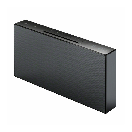
CMT-X3CD
Model Name Using Similar Mechanism
Mechanism Type
Optical Pick-up Block Name
SPECIFICATIONS
Tuner section
FM tuner section:
FM stereo, FM superheterodyne tuner
Tuning range:
87.5 MHz - 108.0 MHz (50 kHz step)
Antenna:
FM lead antenna
Antenna terminals:
8 ohms unbalanced
Speaker section
Speaker system:
Full-range speaker
Passive radiator
Rated impedance:
8 ohms
BLUETOOTH section
Communication system:
BLUETOOTH Standard version 4.0
Output:
BLUETOOTH Standard Power Class 2
Maximum communication range:
*1
Line of sight approx. 10 m
Frequency band:
2.4 GHz band (2.4000 GHz - 2.4835 GHz)
Modulation method:
FHSS
*2
Compatible BLUETOOTH profiles
:
A2DP (Advanced Audio Distribution Profile)
AVRCP (Audio Video Remote Control Profile)
Supported content protection method
SCMS-T method
Singapore Model
Taiwan Model
Korean Model
Thai Model
NEW
T33DS
S76RFS7GP
Supported codec
SBC (Sub Band Codec)
Transmission bandwidth
20 Hz - 20,000 Hz (with 44.1 kHz sampling)
1
*
The actual range will vary depending on factors
such as obstacles between devices, magnetic
fields around a microwave oven, static
electricity, reception sensitivity, antenna's
performance, operating system, software
application, etc.
2
*
BLUETOOTH standard profiles indicate the
purpose of BLUETOOTH communication
between devices.
General
Power requirements:
AC 120 V - 240 V, 50 Hz/60 Hz
(Singapore and Thai models)
AC 110 V - 240 V, 50 Hz/60 Hz (Taiwan model)
AC 220 V - 240 V, 50 Hz/60 Hz (Korean model)
Power consumption:
28 watts
Dimensions (W/H/D) (incl. projecting parts):
Approx. 340 mm × 173 mm × 90 mm
Mass:
Approx. 2.3 kg
Supplied accessories:
Remote (RM-AMU212) (1), FM lead antenna
(1), Operating Instructions (1), Warranty card (1)
(Korean model)
Design and specifications are subject to
change without notice.
Standby power consumption: 0.5 W
(BLUETOOTH network ports off)
BLUETOOTH Standby mode: 5.9 W (BLUETOOTH
network ports on)
PERSONAL AUDIO SYSTEM
Advertisement
Table of Contents

Related Manuals for Sony CMT-X3CD


Summary of Contents for Sony CMT-X3CD
- Page 1 (BLUETOOTH network ports off) Dynamic range: Supported content protection method BLUETOOTH Standby mode: 5.9 W (BLUETOOTH More than 90 dB SCMS-T method network ports on) PERSONAL AUDIO SYSTEM 9-896-051-02 Sony Corporation 2014L33-1 © 2014.12 Published by Sony Techno Create Corporation...
-
Page 2: Table Of Contents
The BLUETOOTH® word mark and logos are registered trademarks owned by BLUETOOTH 2-8. AC Cord Assy (AC1) ............14 SIG, Inc. and any use of such marks by Sony 2-9. PW Board ................ 15 Corporation is under license. 2-10. Speaker Unit (SP1, SP2) ..........16 The N Mark is a trademark or registered trademark of NFC Forum, Inc. -
Page 3: Servicing Notes
CMT-X3CD SECTION 1 SERVICING NOTES The SERVICING NOTES contains important information for servicing. Be sure to read this section before repairing the unit. CAPACITOR ELECTRICAL DISCHARGE PROCESSING NOTES ON HANDLING THE OPTICAL PICK-UP When checking the board, the electrical discharge is necessary for BLOCK OR BASE UNIT the electric shock prevention. - Page 4 CMT-X3CD MODEL IDENTIFICATION DESTINATION ABBREVIATIONS Distinguish by Part No. of model number label stuck on the bottom The following abbreviations for model destinations are used in this side of a main unit. service manual. Note: The printed contents of following fi gure model number label may be different from the model number label of a main unit.
- Page 5 CMT-X3CD ABOUT PARTS REPAIR OF EACH BOARDS 2. When You Plug Power Cord and Turn The Main Unit ON, The Main Unit Won’t Have Sound When each boards installed in this unit are defective, individual electrical parts that the mount is done cannot be replaced. When...
- Page 6 CMT-X3CD Checking Location: – MA Board (Component Side) – +13V from PW board HOW TO EJECT THE DISC WHEN POWER SWITCH TURN OFF • Refer to “SECTION 2. DISASSEMBLY”, remove the loader block from the unit. 2 Take out the disc.
-
Page 7: Disassembly
CMT-X3CD SECTION 2 DISASSEMBLY • This set can be disassembled in the order shown below. 2-1. DISASSEMBLY FLOW 2-2. GRILL ASSY (Page 8) 2-3. LOADER BLOCK (Page 9) 2-4. LOADER ASSY (CDM1), OPU ASSY (OP1) (Page 10) 2-5. MA BOARD, NFC MODULE (Page 11) 2-6. - Page 8 CMT-X3CD Note: Follow the disassembly procedure in the numerical order given. 2-2. GRILL ASSY 1 two screws Note: Please spread a sheet under a unit not to injure front panel. 1 four screws – Rear bottom view – 5 claw...
- Page 9 CMT-X3CD 2-3. LOADER BLOCK 1 four screws 7 loader block 6 flexible flat cable (5P) (XP5) 5 flexible flat cable (24P) (XP3) 2 Remove the loader block in the direction of the arrow. 3 Peel off the adhesive sheet. Note: When installing the flexible flat cable,...
-
Page 10: Loader Assy (Cdm1), Opu Assy (Op1)
CMT-X3CD 2-4. LOADER ASSY (CDM1), OPU ASSY (OP1) 1 four screws 2 Remove the loader block in the direction of the arrow. 3 vibration proof rubber 3 vibration proof rubber 3 vibration proof rubber 4 loader cover 3 vibration proof rubber... -
Page 11: Ma Board, Nfc Module
CMT-X3CD 2-5. MA BOARD, NFC MODULE Note 1: When replacing the MA board or the NFC module, be sure replace both at the same time. The MA board or the NFC mod- ule cannot replace with single. 2 connector 1 flexible flat cable (10P) -
Page 12: Ky Board
CMT-X3CD Ver. 1.1 2-6. KY BOARD 2 connector (XP11) 3 two screws 5 KY board Note: When installing the flexible flat cable, ensure that the colored line is parallel to the connector after insertion. 4 flexible flat cable (10P) (XP7) Insert straight into the interior. -
Page 13: In Board
CMT-X3CD Ver. 1.1 2-7. IN BOARD 7 shield cover assy 3 four screws 8 IN board 2 connector 6 two screws (XP8) 4 shield cover block 5 flexible flat cable (8P) (XP16) 1 connector (XP12) Note 1: When installing the flexible flat cable, ensure that the colored line is parallel to the connector after insertion. -
Page 14: Ac Cord Assy (Ac1)
CMT-X3CD Ver. 1.1 2-8. AC CORD ASSY (AC1) screw hole AC cord 1 AC cord connector (CN501) CN501 PW board Note 1: When installing the AC cord assy (AC1), check the direction of claw of cord bushing and install correctly. -
Page 15: Pw Board
CMT-X3CD 2-9. PW BOARD 1 AC cord connector (CN501) 3 four screws 2 connector (XP1) 4 PW board – Front top view –... -
Page 16: Speaker Unit (Sp1, Sp2)
CMT-X3CD 2-10. SPEAKER UNIT (SP1, SP2) 2 connector (XP7) 1 connector (XP6) – Front bottom view – 3 four screws 3 four screws 6 speaker unit (R-ch) (SP2) 6 speaker unit (L-ch) (SP1) 5 Remove the speaker wire from hole of SPK box R assy. -
Page 17: Fv Board
CMT-X3CD Ver. 1.1 2-11. FV BOARD 6 FV board 2 two claws 2 two claws 5 two screws 4 flexible flat cable (10P) (XP7) 3 Remove the FV board block in the direction of the arrow. 1 connector (XP17) – Front bottom view –... -
Page 18: Test Mode
CMT-X3CD SECTION 3 TEST MODE SOFTWARE VERSION VFD TEST It can confi rm the software version. It can confi rm the fluorescent indicator tube. Procedure: Procedure: 1. Press the [ ] button to turn the power on. 1. Press the [ ] button to turn the power on. -
Page 19: Electrical Check
CMT-X3CD SECTION 4 ELECTRICAL CHECK CD SECTION Note: 1. CD block is basically constructed to operate without adjustment. 2. Use YEDS-18 disc (Part No. 3-702-101-01) unless otherwise indicat- 3. Use an oscilloscope with more than 10 M impedance. 4. Clean the object lens by an applicator with neutral detergent when the signal level is low than specifi... -
Page 20: Troubleshooting
CMT-X3CD SECTION 5 TROUBLESHOOTING 1. Operation Check Flow Check if the voltage at pin 1 and 2 of Power is turned on. Replace the PW board. CON502 on the PW board is +13 V. Replace the FV board, and check if the Replace the MA board. - Page 21 CMT-X3CD – From the page 20 – Check if the AUDIO Check if the P7 (AUDIO IN jack) and IN function and Replace the IN board. P8 (HEADPHONE jack) on the IN board. headphone output is OK. Replace the MA board. (See Note)
-
Page 22: Diagrams
CMT-X3CD SECTION 6 DIAGRAMS 6-1. BLOCK DIAGRAM CMT-X3CD... -
Page 23: Wiring Diagram
CMT-X3CD 6-2. WIRING DIAGRAM CMT-X3CD... - Page 24 CMT-X3CD THIS NOTE IS COMMON FOR PRINTED WIRING BOARDS AND SCHEMATIC DIAGRAMS. • Circuit Boards Location (In addition to this, the necessary note is printed in each block.) NFC module For Printed Wiring Boards. For Schematic Diagrams. Note: Note: • All capacitors are in μF unless otherwise noted. (p: pF) 50 •...
-
Page 25: Printed Wiring Board - Ma Board
CMT-X3CD 6-3. PRINTED WIRING BOARD - MA Board - • See page 24 for Circuit Boards Location. • : Uses unleaded solder. MA BOARD (COMPONENT SIDE) MA BOARD (CONDUCTOR SIDE) CMT-X3CD... -
Page 26: Schematic Diagram - Ma Board (1/6)
CMT-X3CD 6-4. SCHEMATIC DIAGRAM - MA Board (1/6) - MA BOARD (1/6) From Power Board VFD_13V 13V_IN PCON PCON ZD751 ZD751 VCC12 ZMM27/27V ZMM27/27V VCC12 POWER_EN POWER_EN POWER_FRQ1 0.1uF 0.1uF 330pF 330pF POWER_FRQ2 R762 R762 POWER_FRQ1 POWER_FRQ1 4.7K 4.7K -24V... -
Page 27: Schematic Diagram - Ma Board (2/6)
CMT-X3CD 6-5. SCHEMATIC DIAGRAM - MA Board (2/6) - MA BOARD (2/6) 100K 100K 4.7K 4.7K 27MHz/30PPM 27MHz/30PPM I2C_SDA AMP_SDA AMP_SDA DVCC3 R295 R295 TUNER_SDA TUNER_SDA 33pF/50V/NP0 33pF/50V/NP0 33pF/50V/NP0 33pF/50V/NP0 MPEG_TX RF3.3V 47pF/50V/NP0 47pF/50V/NP0 MPEG_RX Put these circuits as F3V3... -
Page 28: Schematic Diagram - Ma Board (3/6)
CMT-X3CD 6-6. SCHEMATIC DIAGRAM - MA Board (3/6) - MA BOARD (3/6) SDRAM SD33 MA10 DQ10 A10/AP DQ10 MA11 DQ11 DQ11 DBA0 DQ12 BA0/A13 DQ12 DBA1 DQ13 BA1/A12 DQ13 DQ14 DQ14 SDCLK DQ15 DRAS# RAS# DQ[0..15] DQ15 DQ[0..15] SD33 SD33 MA[0..11]... -
Page 29: Schematic Diagram - Ma Board (4/6)
CMT-X3CD 6-7. SCHEMATIC DIAGRAM - MA Board (4/6) - MA BOARD (4/6) STB3V3 RTC3V3 FB29 FB29 500/800mA 500/800mA STB3V3 R113 R113 C350 C350 RTC3V3 LL4148 LL4148 CE15 CE15 MCU_RST 47uF/16V 47uF/16V 12Mhz/20ppm 12Mhz/20ppm R114 R114 C113 C113 R190 R190 C112 C112 4.7K... -
Page 30: Schematic Diagram - Ma Board (5/6)
CMT-X3CD 6-8. SCHEMATIC DIAGRAM - MA Board (5/6) - MA BOARD (5/6) SPK_RP R224 R224 10K/1% 10K/1% R226 10K/1% R226 10K/1% C144 100pF/50V/NP0 C144 100pF/50V/NP0 ADC_BCLK 6,11 ADC_BCLK ADC_MCLK 6,11 ADC_MCLK ADC_LRCK 6,11 ADC_LRCK C150 C150 ADC_DATA ADC_DATA 1000pF/50V/X7R 1000pF/50V/X7R... -
Page 31: Schematic Diagram - Ma Board (6/6)
CMT-X3CD 6-9. SCHEMATIC DIAGRAM - MA Board (6/6) - MA BOARD (6/6) EAR_DET EAR_DET COMPATIBLE AMP_13V 2PIN/2.0mm 2PIN/2.0mm R773 R773 220K 220K DVCC3 +3.3VD R775 R775 C530 C530 +3.3VD FB32 FB32 500/200mA 500/200mA FB28 FB28 220K 220K 10uF/16V/X7R 10uF/16V/X7R CE56... -
Page 32: Printed Wiring Boards - In/Fv Boards
CMT-X3CD 6-10. PRINTED WIRING BOARDS - IN/FV Boards - • See page 24 for Circuit Boards Location. • : Uses unleaded solder. IN BOARD FV BOARD (COMPONENT SIDE) (COMPONENT SIDE) IN BOARD (CONDUCTOR SIDE) FV BOARD (CONDUCTOR SIDE) CMT-X3CD... -
Page 33: Schematic Diagram - In/Fv Boards
CMT-X3CD 6-11. SCHEMATIC DIAGRAM - IN/FV Boards - IN BOARD C153 NC/1uF/10V/Y5V C153 NC/1uF/10V/Y5V AGND FM3V3 C114 C114 NC/22pF/50V/NP0 NC/22pF/50V/NP0 12MHz 12MHz XP38 XP38 VDDRF FB14 FB14 4.7nh 4.7nh FRF1 8PIN/2.0mm 8PIN/2.0mm GNDRF IISD XP16 XP16 33pF/50V/NP0 33pF/50V/NP0 8.2K 8.2K... -
Page 34: Printed Wiring Board - Ky Board
CMT-X3CD 6-12. PRINTED WIRING BOARD - KY Board - • See page 24 for Circuit Boards Location. • : Uses unleaded solder. KY BOARD (COMPONENT SIDE) KY BOARD (CONDUCTOR SIDE) CMT-X3CD... -
Page 35: Schematic Diagram - Ky Board
CMT-X3CD 6-13. SCHEMATIC DIAGRAM - KY Board - KY BOARD 10pin/1.0mm 10pin/1.0mm ADC_KEY1 ADC_KEY2 POWER_KEY POWER_KEY POWER_KEY ESD11 ESD11 ADC_KEY2 PESD5V0S1BA/30K/35pF PESD5V0S1BA/30K/35pF TSAB-1 TSAB-1 TSAB-1 TSAB-1 SW1:0V R4 1k R4 1k ESD12 ESD12 ADC_KEY1 TSAB-1 TSAB-1 100pF/50V/NP0 100pF/50V/NP0 PESD5V0S1BA/30K/35pF PESD5V0S1BA/30K/35pF... -
Page 36: Schematic Diagram - Pw Board
CMT-X3CD 6-14. SCHEMATIC DIAGRAM - PW Board - PW BOARD CY502 CY502 C508 C508 0.0022uF(222)400V 0.0022uF(222)400V D555 D555 D556 D556 R5021 R5021 R5022 R5022 R5023 R5023 R5024 R5024 CE501 CE501 CE502 CE502 FR207/2A/1000V FR207/2A/1000V 22uF/450V 22uF/450V 22uF/450V 22uF/450V 150K 150K... -
Page 37: Printed Wiring Board - Pw Board
CMT-X3CD 6-15. PRINTED WIRING BOARD - PW Board - • See page 24 for Circuit Boards Location. • : Uses unleaded solder. PW BOARD (COMPONENT SIDE) PW BOARD (CONDUCTOR SIDE) -
Page 38: Exploded Views
CMT-X3CD SECTION 7 EXPLODED VIEWS Note: • -XX and -X mean standardized parts, so • The mechanical parts with no reference The components identifi ed by mark 0 they may have some difference from the number in the exploded views are not sup- or dotted line with mark 0 are critical for original one. -
Page 39: Loader Section
CMT-X3CD 7-2. LOADER SECTION FFC1 supplied supplied supplied supplied CDM1 Ref. No. Part No. Description Remark Ref. No. Part No. Description Remark 9-885-197-51 SCREW (5) 0 OP1 A-2062-014-A OPU ASSY (S76RFS7GP) 9-885-197-44 RUBBER VIBRATION PROOF (Including RUBBER VIBRATION PROOF) CDM1... -
Page 40: Ma Board Section
CMT-X3CD Ver. 1.1 7-3. MA BOARD SECTION • Bottom view NFC module MA board FFC2 PW board section Note: When replacing the MA board or the NFC module, be sure re- place both at the same time. The MA board or the NFC module cannot replace with single. -
Page 41: Pw Board Section
CMT-X3CD Ver. 1.1 7-4. PW BOARD SECTION rear panel section FFC3 not supplied not supplied not supplied Ref. No. Part No. Description Remark Ref. No. Part No. Description Remark 9-885-197-51 SCREW (5) 0 156 9-885-200-51 BUSHING A-2062-019-A IN BOARD, COMPLETE... -
Page 42: Rear Panel Section
CMT-X3CD Ver. 1.1 7-5. REAR PANEL SECTION • Bottom view not supplied not supplied FFC4 Ref. No. Part No. Description Remark Ref. No. Part No. Description Remark 9-885-197-56 FOOT FOR MAIN (5 pieces, 1 set) 9-885-197-51 SCREW (5) X-2590-354-1 BOTTOM ASSY DS (for BLACK) -
Page 43: Accessories
CMT-X3CD SECTION 8 ACCESSORIES Ref. No. Part No. Description Remark 4-540-126-61 MANUAL, INSTRUCTION (ENGLISH, FRENCH, TRADITIONAL CHINESE) (SP) 4-540-126-71 MANUAL, INSTRUCTION (KOREAN) (KR) 4-540-126-81 MANUAL, INSTRUCTION (TRADITIONAL CHINESE) (TW) 4-540-126-91 MANUAL, INSTRUCTION (THAI) (TH) 9-885-185-38 WIRE, ANT FM (FM lead antenna) - Page 44 CMT-X3CD REVISION HISTORY Ver. Date Description of Revision 2014.09 2014.12 Addition of SHEET (Ref. No. 155), BUSHING (Ref. No. 156) and FLEXIBLE FLAT CABLE (Ref. No. FFC2, FFC3, FFC4) (SMR-14037)