Table of Contents
Advertisement
Please refer to the original service manual for:
CD Mechanism Unit (BRS1C), Order No. PSG1102001CE
Speaker system SB-AKX14LM-K, Order No. PMX1206002CE
CD Stereo System
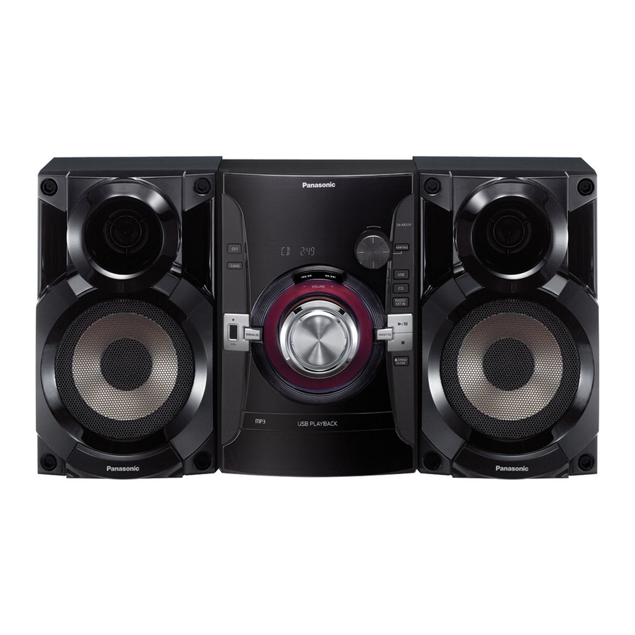
SA-AKX14LM-K
Model No.
Product Color: (K)...Black Type
© Panasonic Corporation 2012. All rights reserved.
Unauthorized copying and distribution is a violation
of law.
PMX1206001CE
Advertisement
Table of Contents
Troubleshooting

Related Manuals for Panasonic SA-AKX14LM-K


Summary of Contents for Panasonic SA-AKX14LM-K
- Page 1 Product Color: (K)...Black Type Please refer to the original service manual for: CD Mechanism Unit (BRS1C), Order No. PSG1102001CE Speaker system SB-AKX14LM-K, Order No. PMX1206002CE © Panasonic Corporation 2012. All rights reserved. Unauthorized copying and distribution is a violation of law.
-
Page 2: Table Of Contents
2.2. Precaution of Laser Diode 8 Service Mode 2.3. Service caution based on Legal restrictions 8.1. Cold-Start 2.4. Handling Precautions for Traverse Unit 8.2. Doctor Mode Table © Panasonic Corporation 2012. All rights reserved. Unauthorized copying and distribution is a violation of law. - Page 3 8.3. Reliability Test Mode (CD Mechanism Unit 18 Printed Circuit Board (BRS1C)) 18.1. CD Servo P.C.B. 8.4. Self-Diagnostic Mode 18.2. Main & Tuner P.C.B. 18.3. Panel, LCD, Remote Sensor & USB P.C.B. 8.5. Self-Diagnostic Error Code Table 18.5. SMPS P.C.B. 8.6.
-
Page 4: Safety Precautions
1 Safety Precautions 1.1. General Guidelines 1. When servicing, observe the original lead dress. If a short circuit is found, replace all parts which have been overheated or damaged by the short circuit. 2. After servicing, see to it that all the protective devices such as insulation barriers, insulation papers shields are properly installed. -
Page 5: Protection Circuitry
1.4. Protection Circuitry The protection circuitry may have operated if either of the following conditions are noticed: No sound is heard when the power is turned on. Sound stops during a performance. The function of this circuitry is to prevent circuitry damage if, for example, the positive and negative speaker connection wires are “shorted”, or if speaker systems with an impedance less than the indicated rated impedance of the amplifier are used. -
Page 6: Safety Parts Information
1.6. Safety Parts Information Safety Parts List: There are special components used in this equipment which are important for safety. These parts are marked by in the Schematic Diagrams, Exploded View & Replacement Parts List. It is essential that these critical parts should be replaced with manufacturer’s specified parts to prevent shock, fire or other hazards. - Page 7 2 Warning 2.1. Prevention of Electrostatic Discharge (ESD) to Electrostatic Sensitive (ES) Devices Some semiconductor (solid state) devices can be damaged easily by static electricity. Such components commonly are called Elec- trostatically Sensitive (ES) Devices. Examples of typical ES devices are integrated circuits and some field-effect transistors and semiconductor "chip"...
-
Page 8: Precaution Of Laser Diode
2.2. Precaution of Laser Diode Caution: This product utilizes a laser diode with the unit turned “on”, invisible laser radiation is emitted from the pickup lens. Wavelength: 790 nm (CD) Maximum output radiation power from pickup: 100 W/VDE Laser radiation from the pickup unit is safety level, but be sure the followings: 1. -
Page 9: Service Caution Based On Legal Restrictions
2.3. Service caution based on Legal restrictions 2.3.1. General description about Lead Free Solder (PbF) The lead free solder has been used in the mounting process of all electrical components on the printed circuit boards used for this equipment in considering the globally environmental conservation. The normal solder is the alloy of tin (Sn) and lead (Pb). -
Page 10: Handling Precautions For Traverse Unit
2.4. Handling Precautions for Traverse Unit The laser diode in the optical pickup unit may break down due to static electricity of clothes or human body. Special care must be taken avoid caution to electrostatic breakdown when servicing and handling the laser diode in the traverse unit. Cautions to Be Taken in Handling the Optical Pickup Unit 2.4.1. -
Page 11: Grounding For Electrostatic Breakdown Prevention
Grounding for electrostatic breakdown prevention 2.4.2. Some devices such as the DVD player use the optical pickup (laser diode) and the optical pickup will be damaged by static electric- ity in the working environment. Proceed servicing works under the working environment where grounding works is completed. 2.4.2.1. -
Page 12: Service Navigation
3 Service Navigation 3.1. Service Information This service manual contains technical information which will allow service personnel’s to understand and service this model. Please place orders using the parts list and not the drawing reference numbers. If the circuit is changed or modified, this information will be followed by supplement service manual to be filed with original service manual. -
Page 13: Specifications
4 Specifications ó i f i l a í é t ó i l a t ) f r Peso l a t é t ° 0 ° 0 x á i t a ó i ó i Consumo de energía en modo normal 58Wh/día (considerando 1 hora de uso al día). - Page 14 5 General/Introduction 5.1. Media Information...
-
Page 15: Location Of Controls And Components
6 Location of Controls and Components 6.1. Remote Control Key Button Operation... - Page 16 6.2. Main Unit Key Button Operation...
-
Page 17: Installation Instructions
7 Installation Instructions 7.1. Speaker and A/C Connection... -
Page 18: Service Mode
8 Service Mode 8.1. Cold-Start Here is the procedure to carry out cold-start or initialize to shipping mode. 1. Unplug AC power cord 2. Press & hold [POWER] button 3. Plug AC power cord while [POWER] button being pressed FL Display will show “_ _ _ _ _ _ _ _” 4. -
Page 19: Doctor Mode Table
8.2. Doctor Mode Table 8.2.1. Doctor Mode Table 1 Item Key Operation FL Display Mode Name Description Front Key Doctor Mode To enter into Doctor Mode In CD Mode: 1. Press [ ] button on main unit follow by [4] and [7] on remote control. - Page 20 8.2.2. Doctor Mode Table 2 Item Key Operation FL Display Mode Name Description Front Key Volume Setting To check the volume setting of a main In Doctor Mode: Check unit. 1. Press [7], [8], [9] button on remote control. Press [7]: VOL50 Volume Press [8]: VOL35 Press [9]: VOL0...
- Page 21 8.2.3. Doctor Mode Table 3 Item Key Operation FL Display Mode Name Description Front Key i. Function: To display result of In Doctor Mode: Self- Adjustment self-adjustment for CD . 1. Press [10] [1] [4] button on remote control . (AJST) This is used for servicing Result Display...
- Page 22 8.3. Reliability Test Mode (CD Mechanism Unit (BRS1C)) Below is the process flow chart of the aging test for the CD Mechanism Unit (BRS1C). OPEN First Track Operation Access OPEN wait First Track for 1 s Play 5 s CLOSE Count up Last Track Operation...
-
Page 23: Self-Diagnostic Mode
8.4. Self-Diagnostic Mode Item Key Operation FL Display Mode Name Description Front Key Self Diagnostic To enter into self diagnostic checking Step 1: Select CD mode Mode (Ensure no disc is inserted). Step 2: Press & hold [ ] follow by ] on main unit for 2 seconds. -
Page 24: Sales Demonstration Lock Function
8.5.2. CD Mechanism Error Code Table (CD Mechanism Unit (BRS1C)) Error Code Diagnostic Contents Description of error Automatic FL Display Remarks CD H15 CD Open Abnormal During operation Press [ ] on main unit for POS_SW_R On fail to be next error. -
Page 25: Troubleshooting Guide
9 Troubleshooting Guide 9.1. Part Location 9.1.1. SMPS P.C.B. AC Inlet: P5701 Fuse: SMPS Control IC: IC5799 Switching Regulator IC: Thermistor: IC5701 TH5860 Photocoupler: PC5702, PC5799 Rectifier Diode D5801, D5802 Photocoupler: PC5720 Connector: Main Transformer: CN5802 T5701 Fig. 1 SMPS P.C.B. - Page 26 9.1.2. Main P.C.B. Resistor Defective R5905 Resistor Defective Resistor Defective R5936 R5928 Audio Digital Amp IC IC5902 Resistor Defective R5926 Voltage Regulator Circuit D2004 Regulator Circuit Q2022 Regulator Circuit Cable Wire D2017 CN2000 Regulator Circuit Voltage Regulator Circuit Q2000 IC2021 Switching Voltage Regulator IC2011 Voltage Regulator...
-
Page 27: Troubleshooting Guide For F61 And/Or F
9.2. Troubleshooting Guide for F61 and/or F76 This section illustrates the checking procedures when upon detecting the error of “F61” and/or “F76” after power up of the unit. It is for purpose of troubleshooting and checking in SMPS & Main P.C.B. Symptom Checking Items Possible Fault(s) - Page 28 D-Amp IC Operation & Control...
- Page 29 1170 ~ 1250 1260 ~ 1450 1460 ~ 1540 1550 ~ 1710 Table 4: F_HOP Control during 10 kHz Step Note: During activating, the 3 control pins namely MUTE_F, MUTE_A and MODE_DA must be used to cover the “Pop” sound cause by F-HOP switching.
-
Page 30: Service Fixture & Tools
10 Service Fixture & Tools Prepare service tools before process service position. Ref. No Service Tools Remarks SFT1 Main P.C.B. (CN2000) - SMPS P.C.B. (CN5802) REX1534(15P Cable Wire) -
Page 31: Disassembly And Assembly Instructions
11 Disassembly and Assembly Instructions • Illustration is based on SA-AKX14PH-K. Caution Note: • This section describes the disassembly and/or assembly procedures for all major printed circuit boards & main compo- nents for the unit. (You may refer to the section of “Main components and P.C.B Locations” as described in the service manual) •... -
Page 32: Disassembly Flow Chart
11.1. Disassembly Flow Chart 11.3.Top Cabinet 11.20. CD Mechanism Unit 11.4. Tuner P.C.B. 11.11. Main P.C.B. (BRS1C) 11.12. Voltage Regulator 11.21. Rear Panel 11.5. Front panel Unit Transistor (Q2022) 11.22. Voltage Selector P.C.B. 11.13. Audio Digital Amp 11.6. Panel P.C.B. IC (IC5902) 11.7. - Page 33 11.2. Main Components and P.C.B. Locations...
-
Page 34: Disassembly Of Top Cabinet
11.3. Disassembly of Top Cabinet Step 4 Slightly lift up both side of Top Cabinet in an outward direction as shown. Step 1 Remove 2 screws on each side. Step 5 Remove the Top Cabinet. Step 2 Remove 5 screws. Step 3 Slightly pull both side of Top Cabinet outwards as arrow shown. -
Page 35: Disassembly Of Front Panel
11.4. Disassembly of Tuner P.C.B. 11.5. Disassembly of Front Panel Unit • Refer to “Disassembly of Top Cabinet”. • Refer to “Disassembly of Top Cabinet”. Step 1 Remove 1 screw. Step 1 Detach 5P Cable Wire at the connector (CN2005) on Main P.C.B. - Page 36 Step 3 Push inwards slightly at the Bottom Chassis as arrow Step 4 Release tabs at bottom. shown and release tab at left side of Front Panel Unit. Step 5 Push inwards slightly at the Bottom Chassis and release tab at right side of Front Panel Unit.
- Page 37 Step 6 Remove the Front Panel Unit 11.6. Disassembly of Panel P.C.B. • Refer to “Disassembly of Top Cabinet”. • Refer to “Disassembly of Front Panel Unit”. Step 1 Remove the Volume Knob. Step 2 Remove the Skip Knob. Step 3 Remove 6 screws.
- Page 38 Step 4 Release catches by following the sequences (1-10). Step 6 Desolder 7 pins at (ZJ600A) on Panel P.C.B.. Step 7 Remove the Panel P.C.B.. Step 5 Lift up to remove the Panel P.C.B. from Front Panel Unit. Caution: During assembling, ensure that Panel P.C.B. is seated properly through the guides &...
-
Page 39: Disassembly Of Usb P.c.b
11.7. Disassembly of Remote Sensor 11.8. Disassembly of USB P.C.B. P.C.B. • Refer to “Disassembly of Top Cabinet”. • Refer to “Disassembly of Front Panel Unit”. • Refer to “Disassembly of Top Cabinet”. • Refer to (Step1) to (Step5) of item 11.6. •... -
Page 40: Disassembly Of Lcd P.c.b
11.9. Disassembly of LCD P.C.B. Caution: During assembling, ensure that LCD Unit is prop- erly located & seated onto the guides. • Refer to “Disassembly of Top Cabinet”. • Refer to “Disassembly of Front Panel Unit”. Step 1 Remove 2 screws. Step 2 Lift up the LCD Unit. -
Page 41: Disassembly Of Cd Lid
11.10. Disassembly of CD Lid 11.11. Disassembly of Main P.C.B. • Refer to “Disassembly of Top Cabinet”. • Refer to “Disassembly of Top Cabinet”. • Refer to “Disassembly of Front Panel Unit”. • Refer to “Disassembly of Front Panel Unit”. Step 1 Remove the spring as arrow shown in order of Step 1 Detach 15P Cable Wire at the connector (CN5802) on sequence (1) to (3). - Page 42 Step 3 Remove 2 screws. Step 5 Detach 9P FFC at the connector (CN2010) on Main Step 4 Detach Main P.C.B. from Rear Panel according to arrow P.C.B.. shown. Step 6 Detach 27P FFC at the connector (CN2706) on Main P.C.B..
- Page 43 11.12. Replacement of Voltage Regu- 11.12.2. Assembly of Voltage Regulator Transistor (Q2022) lator Transistor (Q2022) Step 1 Apply grease to the Heatsink. • Refer to “Disassembly of Main P.C.B.”. Step 2 Fix the Voltage Regulator Transistor (Q2022) on Main P.C.B.. 11.12.1.
-
Page 44: Replacement Of Audio Digital
11.13. Replacement of Audio Digital Step 3 Remove Heatsink Clip. Step 4 Remove Audio Digital Amp IC (IC5902). Amp IC (IC5902) • Refer to “Disassembly of Main P.C.B.”. 11.13.1. Disassembly of Audio Digital Amp IC (IC5902) Step 1 Desolder pins of the Audio Digital Amp IC (IC5902) on the solder side of Main P.C.B.. -
Page 45: Disassembly Of Smps P.c.b
Step 4 Solder pins of the Audio Digital Amp IC (IC5902) on the 11.14. Disassembly of SMPS P.C.B. solder side of Main P.C.B.. • Refer to “Disassembly of Top Cabinet.”. • Refer to “Disassembly of Front Panel Unit”. Step 1 Remove 1 screw. Step 2 Remove 3 screws. - Page 46 Step 4 Flip the SMPS P.C.B. and position it according to dia- 11.15. Replacement of Switching Reg- gram shown. ulator IC (IC5701) Step 5 Place SMPS P.C.B. on an insulated material. Step 6 Desolder 2 Wire pins, TL7 (Black), TL8 (Red). •...
- Page 47 Step 2 Remove 1 screw. Step 4 Solder pins of the Switching Regulator IC (IC5701) on Step 3 Remove the Switching Regulator IC (IC5701). the solder side of SMPS P.C.B.. Caution: Avoid touching the Heatsink A due to its high temperature after prolonged use.
- Page 48 11.16. Replacement of Rectifier Diode Step 3 Remove 1 screw at Switching Regulator IC (IC5701). Step 4 Remove the Heatsink A with Rectifier Diode (D5702). (D5702) Step 5 Remove 1 screw. • Refer to “Disassembly of SMPS P.C.B.”. Step 6 Remove the Rectifier Diode (D5702) from the Heatsink Caution: Avoid touching the Heatsink A due to its high 11.16.1.
- Page 49 11.16.2. Assembly of Rectifier Diode Step 5 Solder pins of the Rectifier Diode (D5702) on the solder side of SMPS P.C.B.. (D5702) Step 6 Solder pins of the Heatsink A on the solder side of Step 1 Apply grease to the Heatsink A. SMPS P.C.B..
- Page 50 11.17. Replacement of Rectifier Diode Step 2 Remove 1 screw at Rectifier Diode (D5801). Step 3 Remove the Rectifier Diode (D5801) from the SMPS (D5801) P.C.B.. • Refer to “Disassembly of SMPS P.C.B.”. Caution: Avoid touching the Heatsink B due to its high temperature after prolonged use.
- Page 51 Step 4 Solder pins of the Rectifier Diode (D5801) on the solder 11.18. Replacement of Rectifier Diode side of SMPS P.C.B.. (D5802) • Refer to “Disassembly of SMPS P.C.B.”. 11.18.1. Disassembly of Rectifier Diode (D5802) Step 1 Desolder pins of the Rectifier Diode (D5802) on the sol- der side of SMPS P.C.B.
- Page 52 11.18.2. Assembly of Rectifier Diode 11.19. Replacement of Regulator (D5802) Diode (D5803) Step 1 Apply grease to the Heatsink B. • Refer to “Disassembly of SMPS P.C.B.”. Step 2 Fix the Rectifier Diode (D5802) on SMPS P.C.B.. Caution: Ensure pins of the Rectifier Diode (D5802) is properly inserted on SMPS P.C.B.
- Page 53 Step 2 Remove 1 screw at Rectifier Diode (D5803). Step 4 Solder pins of the Rectifier Diode (D5803) on the solder Step 3 Remove the Rectifier Diode (D5803) from the SMPS side of SMPS P.C.B. P.C.B.. Caution: Avoid touching the Heatsink B due to its high temperature after prolonged use.
- Page 54 11.20. Disassembly of CD Mecha- Step 3 Remove 3 screws. nism Unit (BRS1C) • Refer to “Disassembly of Top Cabinet”. • Refer to “Disassembly of Front Panel Unit”. Step 1 Detach 15P Cable Wire at the connector (CN5802) on SMPS P.C.B.. Step 4 Detach Voltage Selector P.C.B.
- Page 55 Step 5 Lift up and remove SMPS Inner Chassis Unit. Step 6 Remove 2 screws. Step 7 Lift up & upset the CD Mechanism Unit (BRS1C) as shown. Step 8 Detach 27P FFC at the connector (CN7002) on CD Servo P.C.B.. Step 9 Detach 5P Wire at the connector (CN7001) on CD Servo P.C.B..
-
Page 56: Disassembly Of Rear Panel
11.21. Disassembly of Rear Panel Step 4 Release 2 tabs. • Refer to “Disassembly of Top Cabinet”. Step 5 Remove Rear Panel. • Refer to “Disassembly of Tuner P.C.B.”. Step 1 Remove 6 screws. -
Page 57: Replacement Of Traverse Unit
12 Replacement of Traverse Unit 12.1. Disassembly of Traverse Unit Step 2: Slide the tray out fully. • Refer to “Disassembly of CD Mechanism Unit (BRS1C)”. Caution: Refer to “2.4 Handling Precaution for Traverse Unit” to prevent static damage to the Optical Pickup Unit. Note: 1. - Page 58 Step 4: Release the guide as shown & slide the Traverse Slide Step 6: Lift the Traverse Unit by approximately 45 . Plate to the end. Step 7: Slide out the traverse unit as arrow shown. Step 5: Detach 5P FFC at the connector (CN7003) on CD Servo P.C.B..
-
Page 59: Assembly Of Traverse Unit
12.2. Assembly of Traverse Unit Step 2: Slot the Traverse Unit at approximately 45 into the mecha chassis as arrow shown. Step 1: Release the guide as shown & slide the Traverse Slide Plate to the end. - Page 60 Step 3: Ensure the Traverse Unit seated properly onto the Step 6: Slide the Traverse Slide Plate unit it stop at the Guide. Groove. Step 7: Slot the Tray into the guides as Picture shown. Step 4: Slide Traverse Slide Plate to lock the Traverse Unit as shown.
- Page 61 Step 8: Ensure the guides is align with the groove when sliding 12.3. Disassembly Servo the tray in. P.C.B. • Refer to “Disassembly of CD Mechanism Unit (BRS1C)”. • Refer to “Replacement of Traverse Unit”. Caution: It is required to short the circuit. Step 1: Solder the 3 solder points.
- Page 62 Caution 2: During assembling, desolder the solder points. Step 5 Slightly lift up the CD Servo P.C.B. Step 6 Flip the CD Servo P.C.B. Step 2 Remove 3 screws. Step 3 Desolder 4 pins. Step 4 Detach 5P FFC at the connector (CN7003) on CD Servo P.C.B..
- Page 63 Step 9 Ground the 24P FFC with a short pin.
-
Page 64: Service Position
13 Service Position 13.2. Checking and Repairing of Note: For description of the disassembly procedures, see the Section 11. Panel P.C.B. 13.1. Checking and Repairing of Step 1 Remove Top Cabinet. Main P.C.B. Step 2 Remove Front Panel Unit. Step 3 Attach 5P Cable Wire to the connector (CN2005) on Step 1 Remove Top Cabinet. - Page 65 13.3. Checking and Repairing of LCD 13.4. Checking and Repairing of P.C.B. SMPS P.C.B. Step 1 Remove Top Cabinet. Step 1 Remove Top Cabinet. Step 2 Remove Front Panel Unit. Step 2 Remove Front Panel Unit. Step 3 Position LCD Unit on the insulated material as shown. Step 3 Remove SMPS P.C.B..
-
Page 66: Checking And Repairing Of Cd Servo P.c.b
13.5. Checking and Repairing of CD Servo P.C.B. Step 1 Remove Top Cabinet. Step 2 Remove Front Panel Unit. Step 3 Remove SMPS Chassis Unit. Step 4 Remove CD Mechanism Unit (BRS1C). Step 5 Remove Main P.C.B.. Step 6 Position Front Panel Unit, SMPS Chassis Unit, CD Mechanism Unit (BRS1C), Main P.C.B as diagram shown. Step7 Position Main P.C.B. -
Page 74: Schematic Diagram
17 Schematic Diagram 17.1. Schematic Diagram Notes This schematic diagram may be modified at any time with the development of new technology. Notes: S5701: Voltage ADJ switch (For PH only). S6001: Power switch ( S6002: D.BASS switch. S6003: Manual EQ switch. S6004: Rewind ( ) switch. -
Page 89: Appendix Information Of Schematic Diagram
19 Appendix Information of Schematic Diagram Voltage & Waveform Chart 19.1. Note: • Indication Voltage Values are in standard values for the unit measured by the DC electronic circuit tester (high-impedance) with the chassis taken as standard. Therefore, there may exist some errors in voltage values, depending on the internal impedance of the DC circuit tester. •... - Page 90 19.2. Main P.C.B. (1/2) IC2003 REF NO. MODE POWER ON STANDBY IC2003 REF NO. MODE POWER ON STANDBY IC2003 REF NO. MODE POWER ON STANDBY IC2003 REF NO. MODE POWER ON STANDBY IC2003 REF NO. MODE POWER ON STANDBY IC2006 REF NO.
- Page 91 19.3. Main P.C.B. (2/2) IC2201 REF NO. MODE CD PLAY STANDBY IC5902 REF NO. MODE CD PLAY -11.0 34.5 -32.9 -24.6 35.6 -34.0 -31.0 -34.0 34.6 -34.0 -34.0 34.0 STANDBY -11.0 34.5 -32.9 -24.6 35.6 -34.0 -31.0 -34.0 34.6 -34.0 -34.0 34.0 IC5902 REF NO.
- Page 92 19.4. LCD P.C.B. IC900 REF NO. MODE POWER ON STANDBY IC900 REF NO. MODE POWER ON STANDBY IC900 REF NO. MODE POWER ON STANDBY Q900 REF NO. MODE POWER ON STANDBY SA-AKX14 LCD P.C.B. 19.5. Tuner P.C.B. IC52 REF NO. MODE TUNER SA-AKX14...
- Page 93 19.6. SMPS P.C.B. IC5701 REF NO. MODE POWER ON 164.8 19.1 STANDBY 164.8 19.1 IC5799 REF NO. MODE POWER ON 11.0 164.2 STANDBY 11.0 164.2 IC5801 REF NO. MODE POWER ON -30.0 STANDBY -30.0 IC5899 REF NO. MODE POWER ON STANDBY Q5720 Q5721...
- Page 94 19.7. Waveform Table 0.1Vp-p(200usec/div) 0.2Vp-p(100usec/div) 4Vp-p(500usec/div) 3.2Vp-p(100usec/div) 0.4Vp-p(200usec/div) 2.95Vp-p(10usec/div) 0.1Vp-p(200usec/div) 1.4Vp-p(100usec/div) 3.6Vp-p(200usec/div) 100Vp-p(1usec/div) 1.5Vp-p(500usec/div) 1.4Vp-p(1msec/div)
-
Page 95: Illustration Of Ics, Transistor And Diode
Illustration of ICs, Transistor and Diode 19.8. *Este material se encuentra sin programar, debe ser programado. C0DBAYY01122 (8P) C0ABBB000067 (8P) C1BB00001151 (32P) REP4780A (20P) No.1 No.1 No.1 No.1 No.1 C0GBY0000117 C3EBEY000037 (8P) MIP2F20MSSCF (8P) C0DBFYY00049 C3EBFC000042 * MN101EF16KXM (100P) No.1 B1BACG000048 C0DAZYY00039 C5HACYY00004 (7P) -
Page 96: Terminal Function Of Ics
Terminal Function of ICs 19.9. IC2003 (*MN101EF16KXW): IC 19.9.1. Terminal Name Function MICRO-PROCESSOR - No Connection EE_CS O EEPROM IC Chip select * Este material no se encuentra programado, se debe programar. EE_SCL O EEPROM IC Serial clock Terminal Name Function EE_SDA I/O EEPROM IC Serial data... - Page 97 IC900(C0HBA0000295): IC FL 19.9.2. Driver Terminal Name Function Chip Selection Input Read Clock Input Write Clock Input DATA I/O Serial Data Input Negative Power Supply VLCD LCD Power Input Positive Power Supply O Tone Frequency Output Pair COM0 O Common Output 0 COM1 O Common Output 1 COM2...
- Page 101 20.1.3. Mechanical Replacement Part List Safety Ref. Part No. Part Name & Qty Remarks Description Safety Ref. Part No. Part Name & Qty Remarks 18-1 RMGX0033A-K CD LID CUSHION Description 18-2 RGK2307-KL CD LID CABINET 18-3 RKAX0042-K LEG CUSHION CHASSIS 18-4 RKW0984-KL UNDER WINDOW...
- Page 102 Safety Ref. Part No. Part Name & Qty Remarks Description TRAVERSE DECK RD-DDL081-PX BRS1C CD UNIT RAEX1033Z-V TRAVERSE ASS'Y XTN2+6GFJ SCREW PACKING MATERI- RPGM0271-1 PACKING CASE RPNM0240T/B POLYFOAM RPFX0198 MIRAMAT SHEET ACCESSORIES N2QAYB000636 REMOTE CONTROL K2CB2YY00059 AC CORD RQTM0187 O/I BOOK N1DYYYY00010 AM LOOP ANTENNA RSAX0002...
- Page 103 20.2. Electrical Replacement Part List...
- Page 104 Safety Ref. no.Part No. Part Name & Description QR5802 B1GDCFGA0018 TRANSISTOR K5D802APA008 FUSIBLE QR5810 B1GBCFLL0037 CHIP TRANSISTOR R5702 D0GZ333JA012 CHIP RESISTOR RAIM12X140A CONJUNTO SMPS AKX14 para uso de CS R5703 D0GZ333JA012 CHIP RESISTOR REPM12X140A CONJUNTO MANUAL SMPS AKX14 R5704 ERJ8GEYJ224V CHIP RESISTOR C5700 F1BAF471A013...
- Page 105 W5517 Z-W6NL ALAMBRE JUMPER C2113 F1H0J1050012 CHIP CAPACITOR W5518 Z-W6NL ALAMBRE JUMPER C2114 F1H0J1050012 CHIP CAPACITOR W5519 Z-W6NL ALAMBRE JUMPER C2115 F1J1A106A043 CHIP CAPACITOR W5520 Z-W6NL ALAMBRE JUMPER C2116 F1J1A106A043 CHIP CAPACITOR W5521 Z-W6NL ALAMBRE JUMPER C2123 F1H1A224A007 CHIP CAPACITOR W5522 Z-W6NL ALAMBRE JUMPER...
- Page 106 D2301 DA2J10100L DIODE R2159 ERJ3GEYJ101V CHIP RESISTOR IC2003 MN101EF16KXW IC MICROP VE este material debe ser grabado. R2163 ERJ3GEYJ102V CHIP RESISTOR IC2006 C3EBEY000037 IC EEPROM R2164 ERJ3GEYJ101V CHIP RESISTOR IC2009 C0DBFYY00049 ICs For Power Supply • R2165 ERJ3GEYJ102V CHIP RESISTOR IC2011 C0DBAYY01122 ICS FOR POWER SUPPLY...
- Page 107 C5946 F2A1A101A184 capacitor electrolitico C5983 F2A1H1R0A213 CAPACITOR ELECTROLITICO R5947 ERJ1TYJ220U CHIP RESISTOR C5989 ECQV1H474JL3 CAPACITOR R5950 ERJ3GEYJ562V CHIP RESISTOR C5990 ECQV1H474JL3 CAPACITOR R5951 ERJ3GEYJ562V CHIP RESISTOR L5900 J0JKB0000020 EMIBEADCORER TH5900 D4CC11040013 CHIP TERMISTOR Q2035 B1BABG000007 TRANSISTOR W5301 ERJ6GEY0R00V CHIP JUMPER R2333 ERG2SJ471E METAL OXIDE FILM RESISTOR...
- Page 108 C2235 F1J1C106A059 CHIP CAPACITOR C2238 F1J1A106A043 CHIP CAPACITOR D2017 DZ2J07500L DIODO QR2001 B1GBCFJJ0051 TRANSISTOR R2017 ERJ3RBD1001V CHIP RESISTOR R2175 ERJ3GEYJ103V CHIP RESISTOR R2195 D0GB101JA008 CHIP RESISTOR R2218 ERJ3GEY0R00V CHIP JUMPER R2223 ERJ3GEYJ823V CHIP RESISTOR R2227 ERJ3GEYJ823V CHIP RESISTOR R2234 ERJ3GEYJ472V RESISTENCIA CHIP PEL CULA R2350 ERJ3GEYJ393V...