Table of Contents
Advertisement
Quick Links
Please refer to the original service manual for:
CD Mechanism Unit (BRS12C), Order No. PSG1303059AE
Speaker system SB-AKX220PN/SB-AKX440PN, Order No. PSG1601002CE
TABLE OF CONTENTS
1 Safety Precautions----------------------------------------------- 3
1.1. General Guidelines---------------------------------------- 3
1.2. Before Repair and Adjustment ------------------------- 4
1.3. Protection Circuitry ---------------------------------------- 4
1.4. Caution For AC Cord ------------------------------------- 5
1.5. Safety Parts Information --------------------------------- 5
2 Warning -------------------------------------------------------------- 6
to Electrostatically Sensitive (ES) Devices---------- 6
2.2. Precaution of Laser Diode------------------------------- 6
(PbF)---------------------------------------------------------- 7
2.4. Handling Precautions for Traverse Unit-------------- 7
prevention --------------------------------------------------- 8
PAGE
SA-AKX320E
Model No.
SA-AKX520E
Product Color: (K)...Black Type
(W)...White Type (For SA-AKX320)
3 Service Navigation -----------------------------------------------9
3.1. Service Information ----------------------------------------9
4 Specifications ---------------------------------------------------- 10
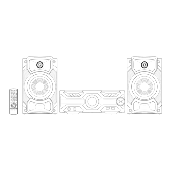
5 Location of Controls and Components------------------ 11
6 Service Mode ----------------------------------------------------- 12
6.1. Cold-Start -------------------------------------------------- 12
6.2. Sales Demonstration Lock Function ---------------- 12
6.3. Doctor Mode Table--------------------------------------- 13
6.4. Self-Diagnostic Mode ----------------------------------- 15
6.5. Self-Diagnostic Error Code Table -------------------- 15
7 Troubleshooting Guide --------------------------------------- 17
7.2. Bluetooth® Pairing Failure----------------------------- 19
7.3. No Key Function------------------------------------------ 20
© Panasonic Corporation 2019. All rights reserved.
Unauthorized copying and distribution is a violation
of law.
PSG1902001CE
CD Stereo System
PAGE
Advertisement
Table of Contents

Related Manuals for Panasonic SA-AKX320E


Summary of Contents for Panasonic SA-AKX320E
-
Page 1: Table Of Contents
7.2. Bluetooth® Pairing Failure----------------------------- 19 2.5. Grounding electrostatic breakdown 7.3. No Key Function------------------------------------------ 20 prevention --------------------------------------------------- 8 7.4. FL Show “No Device” at USB selector Only ------ 21 © Panasonic Corporation 2019. All rights reserved. Unauthorized copying and distribution is a violation of law. - Page 2 7.5. No Sound coming out from All speakers ----------- 22 7.6. No Sound in Tuner and Aux Mode------------------- 23 7.7. No Play or no sound in CD Mode ------------------- 24 8 Disassembly and Assembly Instructions --------------- 25 8.1. Types of Screws ------------------------------------------ 25 8.2.
-
Page 3: Safety Precautions
1 Safety Precautions 1.1. General Guidelines 1. IMPORTANT SAFETY NOTICE There are special components used in this equipment which are important for safety. These parts are marked by in the Schematic Diagrams, Circuit Board Layout, Exploded Views and Replacement Parts List. It is essential that these critical parts should be replaced with manufacturer’s specified parts to prevent X-RADIATION, shock, fire, or other hazards. -
Page 4: Before Repair And Adjustment
1.2. Before Repair and Adjustment Disconnect AC power to discharge AC capacitor (in SMPS Module) as indicate below diagram through a 10 Ω, 1 W resistor to ground. Figure 1-2 Caution: DO NOT SHORT-CIRCUIT DIRECTLY (with a screwdriver blade, for instance), as this may destroy solid state devices. After repairs are completed, restore power gradually using a variac to avoid overcurrent. -
Page 5: Caution For Ac Cord
1.4. Caution For AC Cord 1.5. Safety Parts Information Safety Parts List: There are special components used in this equipment which are important for safety. These parts are marked by in the Schematic Diagrams, Exploded View & Replacement Parts List. It is essential that these critical parts should be replaced with manufacturer’s specified parts to prevent shock, fire or other hazards. -
Page 6: Warning
2 Warning 2.1. Prevention of Electrostatic Discharge (ESD) to Electrostatically Sensi- tive (ES) Devices Some semiconductor (solid state) devices can be damaged easily by static electricity. Such components commonly are called Elec- trostatically Sensitive (ES) Devices. The following techniques should be used to help reduce the incidence of component damage caused by electrostatic discharge (ESD). -
Page 7: General Description About Lead Free Solder (Pbf)
Figure 2-1 2.3. General description about Lead Free Solder (PbF) The lead free solder has been used in the mounting process of all electrical components on the printed circuit boards used for this equipment in considering the globally environmental conservation. The normal solder is the alloy of tin (Sn) and lead (Pb). -
Page 8: Grounding For Electrostatic Breakdown Prevention
4. The antistatic FFC is connected to the new optical pickup unit. After replacing the optical pickup unit and connecting the flexi- ble cable, cut off the antistatic FFC. Figure 2-2 2.5. Grounding for electrostatic breakdown prevention • As for parts that use optical pick-up (laser diode), the optical pick-up is destroyed by the static electricity of the working environ- ment. -
Page 9: Service Navigation
If the circuit is changed or modified, this information will be followed by supplement service manual to be filed with original service manual. 3.1.1. Software Update Panasonic may release updated software for this system that may add or improve the way a feature operates. For more details, refer to the following website. After servicing, please perform firmware update. http://panasonic.jp/support/global/cs/... -
Page 10: Specifications
Operating temperature range 0 °C to +40 °C Operating humidity range 35% to 80% RH System: SC-AKX320E-K (no condensation) Main Unit: SA-AKX320E-K Speakers: SB-AKX220PNK Amplifier section RMS output power stereo mode System: SC-AKX320E-W (For AKX520) Main Unit: SA-AKX320E-W 325 W per channel (3 Ω),... -
Page 11: Location Of Controls And Components
5 Location of Controls and Components... -
Page 12: Service Mode
6 Service Mode 6.1. Cold-Start Item Key Operation FL Display Mode Name Description Front Key Cold Start To carry out cold-start or initialize 1. Unplug AC power cord. to shipping mode 2. Press & hold [POWER] button. 3. Plug in AC power cord while [POWER] button being pressed. -
Page 13: Doctor Mode Table
6.3. Doctor Mode Table Recommend to use remote control with numeric button, example AKX/MAX. 6.3.1. Doctor Mode Table 1 Item Key Operation FL Display Mode Name Description Front Key Doctor Mode 1. Press [ ] button on main unit follow by [4] and [7] on remote control. - Page 14 6.3.2. Doctor Mode Table 2 Item Key Operation FL Display Mode Name Description Front Key Volume Setting To check the volume setting of the In Doctor Mode: Check main unit. 1. Press [7], [8], [9] button on the remote control. Press [7]: VOL50 Volume Press [8]: VOL35...
-
Page 15: Self-Diagnostic Mode
6.4. Self-Diagnostic Mode Item Key Operation FL Display Mode Name Description Front Key Self Diagnostic c i t Mode (Ensure no disc is inserted). Step 2: Press & hold [ ] button follow by [ ] on main unit for 2 seconds. Error Code System will perform a check on c i t... - Page 16 6.5.2. CD Mechanism Error Code Table Item Key Operation Solution FL Display (PCB exchange repair) Mode Name Description Front Key Error Code Diagnosis Contents: Press [ ] on main unit Check following: CD H15 CD Open Abnormal for next error. 1.
-
Page 17: Troubleshooting Guide
7 Troubleshooting Guide 7.1. No Power (No LED Display + No Response) Press Power Button of Unit or Remote Control to Turn ON the Unit No Display on FL Panel Check IC1005 Replace Measured +3.3V at IC1005 pin2 Check Fuse Change (F1) = 0 ohm SMPS... - Page 18 Check Point SMPS PCB Check Point Main PCB...
-
Page 19: Bluetooth® Pairing Failure
® 7.2. Bluetooth Pairing Failure Turn ON the Unit Press [ PAIRING] on the Set or Remote Control Display " BLUETOOTH" Do the Cold Start Blinking "PAIRING' will AC Plug-out. Press display, during and Hold "Power" Pairing check/select on button on smartphone or other Main set then ac devices the "EUT"... -
Page 20: No Key Function
7.3. No Key Function Press Power Button or CD Door Open of Unit to Turn ON the Unit No Display on FL Panel Go to Use remocon to troubleshoot for turn ON the set no power FL Display Check Panel P.C.B, Press remocon IR6500, pin3... -
Page 21: Fl Show "No Device" At Usb Selector Only
7.4. FL Show “No Device” at USB selector Only Press Power Button of Unit or Remote Control to Turn ON the Unit Select USB A or USB B selector, connect USB device, No TOC USB-B_5V at CN2503 Check IC2502 (USB Replaced IC2501 or pin #7.(USB-A_5V at B) or IC2501 (USB... -
Page 22: No Sound Coming Out From All Speakers
7.5. No Sound coming out from All speakers Press Power Button of Unit or Remote Control to Turn ON the Unit No Audio in both high and low channel at All Selector Check 1.5V on Change Pin 13, 14 at IC6500 Check SOC(IC2001) IC6500... -
Page 23: No Sound In Tuner And Aux Mode
7.6. No Sound in Tuner and Aux Mode Press Power Button of Unit or Remote Control to Turn ON the Unit Check Tun-Int Change pin 18 on IC52. IC52 on OK = <0.3V Tuner pcb Switch to Tuner (FM Mode) Check if antenna is Change Check Tun_Rst... -
Page 24: No Play Or No Sound In Cd Mode
No Play or no sound in CD Mode 7.7. Press Power Button of Unit or Remote Control to Turn ON the Unit Switch to CD Mode Press Play FL Change Traverse Unit Output has sound problem Change Check IC2100 I2S IC2001 waveform existence pin 81-83... -
Page 25: Disassembly And Assembly Instructions
8 Disassembly and Assembly Instructions • Illustration is based on SA-AKX520E. Caution Note: • This section describes the disassembly and/or assembly procedures for all major printed circuit boards & main compo- nents for the unit. (You may refer to the section of “Main components and P.C.B Locations” as described in the service manual) •... -
Page 26: Disassembly Flow Chart
8.2. Disassembly Flow Chart Top Cabinet Front Panel Unit Rear Panel Main P.C.B. Panel P.C.B. SMPS Module USB P.C.B. CD Mechanism Button P.C.B. Unit CD Interface Mic P.C.B. P.C.B. (For AKX520) 8.3. Main Components and P.C.B. Locations... -
Page 27: Disassembly Of Top Cabinet
8.4. Disassembly of Top Cabinet Step 5 Lift up to remove Top Cabinet. Step 1 Remove 2 screws. Step 2 Remove 2 screws. 8.5. Disassembly of Front Panel Unit • Refer to “Disassembly of Top Cabinet”. Step 1 Lift up Wire Clamper. (For AKX520) Step 2 Detach 5P Wire at connector (CN2507) on Main P.C.B.. -
Page 28: Disassembly Of Panel P.c.b
8.6. Disassembly of Panel P.C.B. Step 8 Release tabs at bottom of unit. • Refer to “Disassembly of Top Cabinet”. • Refer to “Disassembly of Front Panel Unit”. Step 1 Remove Multi Control Knob. Step 9 Remove Front Panel Unit as arrow shown. Step 2 Remove 4 screws. -
Page 29: Disassembly Of Usb P.c.b
8.8. Disassembly of Button P.C.B. Step 7 Detach 3P Wire at connector (CN6204) on Panel P.C.B.. Step 8 Remove Panel P.C.B.. • Refer to “Disassembly of Top Cabinet”. • Refer to “Disassembly of Front Panel Unit”. • Refer to “Disassembly of Panel P.C.B.”. Step 1 Remove 3 screws. -
Page 30: Disassembly Of Rear Panel
8.10. Disassembly of Rear Panel 8.11. Disassembly of Main P.C.B. • Refer to “Disassembly of Top Cabinet”. • Refer to “Disassembly of Top Cabinet”. • Refer to “Disassembly of Rear Panel”. Step 1 Remove 5 screws. Step 1 Remove 2 screws. Step 2 Release catch. -
Page 31: Disassembly Of Smps Module
8.12. Disassembly of SMPS Module Step 7 Lift up Wire Clamper. (For AKX520) Step 8 Detach 5P Wire at connector (CN2507) on Main P.C.B.. • Refer to “Disassembly of Top Cabinet”. (For AKX520) • Refer to “Disassembly of Rear Panel”. Step 9 Detach 24P FFC at connector (P5002) on Main P.C.B.. -
Page 32: Disassembly Of Cd Interface P.c.b
8.14. Disassembly of CD Interface P.C.B. • Refer to “Disassembly of Top Cabinet”. • Refer to “Disassembly of Rear Panel”. • Refer to “Disassembly of CD Mechanism Unit”. Step 1 Remove 2 screws. Step 2 Desolder pins of the motor (M7301). Step 3 Desolder pins of the motor (M7302). -
Page 33: Service Position
9 Service Position 9.2. Checking of SMPS Module Note: Refer to Section 8 for disassembly instruction for the related parts. Step 1 Remove Top Cabinet. 9.1. Checking of Panel P.C.B. and Step 2 Remove Rear Panel. Step 3 Remove SMPS Module. Main P.C.B. -
Page 34: Block Diagram
PW_SW5V PW_5V CN2500 P6200 I_CLOSE_SW PW_SYS_3R3V CN2500 P6200 PW_STBY3R3V +3.3V 3.3V 3.3V PW_3R3V CN2500 P6200 PW_SW3R3V +3.3V 3.3V 3.3V O_LD_CW O_LD_CCW CD INTERFACE P.C.B. O_PCONT_BT O_USB_A_PCONT O_USB_B_PCONT USB-B USB-B USB-A USB-A TO POWER SUPPLY BT PCONT BT PCONT SA-AKX320E, SA-AKX520E... - Page 35 USB5V USB PORT B XIN_PLL CN6901 CN2503 G_USB_B_D- USB_B_D- (PLAY) X2001 CN6901 CN2503 G_USB_B_D+ XOUT_PLL USB_B_D+ Q2500 D6901 USBLED_B CN6901 CN2503 USB_B_LED_5V SWITCH QR2500 LED DRIVE O_USB_B_LED D6902 Q2501 USBLED_A CN6901 CN2503 USB_A_LED_5V SWITCH QR2501 LED DRIVE O_USB_A_LED SA-AKX320E, SA-AKX520E...
-
Page 36: Audio
DC DETECT JK52 CIRCUIT VALID 4 /RESET 4 AMI DCLK 17 I_I2S_BCK_TUN Q6001,Q6002 Q6007,Q6300 AM ANT DFS 14 I_I2S_LRCK_TUN RST 5 O_TUN_RST GCGPO2 18 I_TUN_INT DOUT I_I2S_SDA_TUN SDIO 8 76 IO_SDA0 SCLK 7 75 O_SCL0 16 /FAULT I_DC_DET_AMP SA-AKX320E, SA-AKX520E... -
Page 37: Power Supply
USB-B /OC 3 USB-B FROM/TO SYSTEM CONTROL IC2501 HIGH SIDE SWITCH USB OVC PW 5V VOUT USB OVC USB-A /OC 3 USB-A PW USBA 5V PW USBA 5V VIN 5 PW 5V, PW CD5V SYSTEM CONTROL PW 5V SA-AKX320E, SA-AKX520E... -
Page 38: Wiring Connection Diagram
MIC P.C.B. (For AKX520) CON2 CN1002 CN6902 CN6901 CN2507...AKX520 CN2500 USB P.C.B. CN2503 P5002 TO OPTICAL PICKUP UNIT (CD MECHANISM UNIT) SMPS MODULE MAIN P.C.B. CN7002 P5001 CD INTERFACE P.C.B. CN7001 TO CD LOADING P.C.B. (CD MECHANISM UNIT) SA-AKX320E, SA-AKX520E WIRING CONNECTION DIAGRAM... -
Page 39: Schematic Diagram
12 Schematic Diagram 12.1. Schematic Diagram Notes • This schematic diagram may be modified at any time with the development of new technology. Notes: S6206: Power switch ( S6207: Open/Close switch ( ). S6208: Stop ( ) / DJ5 switch. S6209: Play/Pause ( / ) / DJ6 switch. -
Page 40: Main (Bluetooth) And Main (Cd Fe) Circuit
12.2. Main (Bluetooth) and Main (CD FE) Circuit SCHEMATIC DIAGRAM - 1 MAIN (BLUETOOTH) CIRCUIT MAIN (CD FE) CIRCUIT OPEN_SW INNER_SW CLOSE_SW C5009 PW_CD5V LB5003 C5010 J0JHC0000045 (WITH TAPE REQUEST BY PRODUCTION) 0.01U P5001 +4.6V LDO 200mA MAX RATED 100mA LD_CCW K1MY10AA0267 (AKX300/500 HAND INSERT CONNECTOR) -
Page 41: Main (Dsp), Main (Tuner) And Main (Damp)
12.3. Main (DSP), Main (Tuner) and Main (DAMP) SCHEMATIC DIAGRAM - 2 MAIN (DSP) CIRCUIT MAIN (TUNER) CIRCUIT AUX_IN JK6002 K2HA2YYA0009 LB6501 J0JYC0000656 PW_3R3V 100P 680P R6146 DGND C6099 C6111 X6500 R6133 H0J245500110 8.2K R6134 R6147 8.2K C6115 100P C6112 R6502 C6116 J0JYC0000656... -
Page 42: Main (Regulator) Circuit
12.4. Main (Regulator) Circuit SCHEMATIC DIAGRAM - 3 MAIN (REGULATOR) CIRCUIT IC1004 C0DBGYY00911 IC1005 C0DBGYY03909 DC+3.3V LDO FOR SOC DC+1.6V VOUT VIN LDO NEAR SOC C1025 C1048 C1049 0.1U 400mA MAX PW_SOC_1R5V SMPS 9 PIN WIRE PW_SOC_1R5V R1067 J0JYC0000656 PW_SYS_5V PW_BT_5V DZ2J150M0L DA2J10100L... -
Page 43: Main (Usb) Circuit
12.5. Main (USB) Circuit SCHEMATIC DIAGRAM - 4 MAIN (USB) CIRCUIT DSA200100L Q2500 USB REC 100K LED CIRCUIT MAIN-PANEL USB B HI SIDE SWITCH 0.5A CONNECTOR USB_B_LED IC2502 C0DBZYY00716 USB-B USB WIRE CLAMPER PW_USB5V - MIN PATTERN WIDTH=0.5mm, 600mA 0.1U USB SUPPLY - MIN PATTERN WIDTH=0.5MM,600mA C2507 VOUT... -
Page 44: Main (Micon) Circui
12.6. Main (MICON) Circui SCHEMATIC DIAGRAM - 5 MAIN (MICON) CIRCUIT IC2003 TZQA01BB6E...AKX320 R3105 TZQA01BB5E...AKX520 G_MIC_SDO PIN105 G_I2S_WCK RX2007 DI(DQ0) G_I2S_BCK R5080 PIN80 LB2006 WP#(DQ2) G_I2S_SDO0 2.2K J0JYC0000656 DO(DQ1) HOLD#(DQ3) R2039 DSP_SDA CR_TIMER PW_XSW3R3V_FLASH C12019 DSP_SCL 560K DSP_RESET C2020 R2193 DSP_MUTE BT_HOST_WAKE CL2009... -
Page 45: Panel (Fl) Circuit
12.7. Panel (FL) Circuit SCHEMATIC DIAGRAM - 6 PANEL (FL) CIRCUIT DP6300 R6305 C6313 C6307 0.1U C16307 DGND R6303 1.2K C16302 C16300 R6318 C6302 C6300 D6302 D6301 R6313 2.7K Q6302 B1HFCDE00002 R6312 DGND DGND DGND C16331 C16330 C6330 C6331 B3RAD0000226 IR6301 REM_IN PW_STBY3R3V... -
Page 46: Panel (Jog Led) Circuit
12.8. Panel (Jog LED) Circuit SCHEMATIC DIAGRAM - 7 PANEL (JOG LED) CIRCUIT R6219 R6218 R6220 R6221 2.2K 3.3K 4.7K 6.8K KEY2_1 DGND P6200 K1MN17B00032 LED_BLUE LED_BLUE LED_RED LED_RED DGND DGND LED_GREEN LED_GREEN VOL_JOG VOL_JOG DGND FL_DIN FL_DIN FL1_CS FL1_CS FL_CLK FL_CLK REM_IN... -
Page 47: Usb, Button, Mic And Cd Interface Circuit
12.9. USB, Button, Mic and CD Interface Circuit SCHEMATIC DIAGRAM - 8 USB CIRCUIT BUTTON CIRCUIT 0.1U C16901 C6901 USB5V R6215 R6216 R6217 R6901 1.8K 1.2K 1.8K USB_A_D- DGND JK6901 R6902 KEY2_1 USB_A_D+ K1FY104A0054 R6910 KEY2 B3AAA0001243 DGND DGND D6902 R6903 CN6201 R6908... -
Page 48: Printed Circuit Board
13 Printed Circuit Board 13.1. Main P.C.B. (Side A) MAIN P.C.B. (SIDE A) SA-AKX320, SA-AKX520... -
Page 49: Main P.c.b. (Side B)
13.2. Main P.C.B. (Side B) MAIN P.C.B. Q6002 L6005 R6057 Q6007 CN1002 C6027 R6132 C6068 R1083 R6098 C6012 R6070 R1088 C6522 L6002 C6591 LB6000 C6500 C6521 R6011 C6025 R6072 C6030 D1008 LB6001 R6090 R6531 R6581 R1044 C6033 R6532 C6553 R6001 C1041 C1018 R1076... -
Page 50: Panel P.c.b
13.3. Panel P.C.B. PANEL P.C.B. S6209 S6219 S6212 CK6010 S6206 R6218 R6209 R6030 CK6011 R6807 R6221 R6210 R6206 R6219 R6220 CK6012 R6031 S6222 S6221 S6220 S6211 S6210 S6207 S6208 R6032 CK6013 CK6014 R6033 R6034 QR6021 CK6015 R6811 IR6301 C6306 DP6300 C16306 C6209 D6040... -
Page 51: Usb, Button, Mic (For Akx520) And Cd Interface P.c.b
13.4. USB, Button, Mic (For AKX520) and CD Interface P.C.B. USB P.C.B. BUTTON P.C.B. CN6902 R6910 CN6901 R6908 R6909 D6902 D6901 JK6901 JK6902 S6218 C6905 C6906 C6907 C6908 C16905 C16906 C16907 C16908 W6902 R6215 S6216 S6215 S6217 MIC P.C.B. (For AKX520) CD INTERFACE P.C.B. -
Page 52: Voltage And Waveform Measurement
REF NO. MODE POWER ON Q1008 Q1010 Q2500 Q2501 Q6002 REF NO. MODE POWER ON SA-AKX320E, SA-AKX520E MAIN P.C.B. Q6301 REF NO. MODE POWER ON SA-AKX320E, SA-AKX520E PANEL P.C.B. IC1042 IC1401 REF NO. MODE POWER ON Note : VALUE IS BASE ON SCHEMATIC CIRCUIT... -
Page 53: Exploded View And Replacement Parts List
15 Exploded View and Replacement Parts List 15.1. Electrical Replacement Parts List Safety Ref. Part No. Part Name & Qty Remarks Description Safety Ref. Part No. Part Name & Qty Remarks IC2002 C0EBY0000664 (E.S.D) Description IC2003 TZQA01BB6E FLASH (E.S.D) PRINTED CIRCUIT WITH DATA 320E-K... - Page 54 Safety Ref. Part No. Part Name & Qty Remarks Safety Ref. Part No. Part Name & Qty Remarks Description Description L6005 G0A100K00006 CHOKE COIL 320E-K Q6007 B1ABCF000176 TRANSISTOR 320E-W Q6300 B1ABCF000176 TRANSISTOR L6300 G0C100M00013 CHOKE COIL 520E-K QR1003 B1GBCFJJ0051 TRANSISTOR L6301 G0C100M00013 CHOKE COIL...
- Page 55 Safety Ref. Part No. Part Name & Qty Remarks Safety Ref. Part No. Part Name & Qty Remarks Description Description C1049 F1G1H104A983 0.1uF C2513 F1H1H102B047 1000pF 520E-K C1051 F2A1C1010033 100uF C2514 F1H1H102B047 1000pF 520E-K C1052 F2A1C221B456 220uF C2515 F1H1H102B047 1000pF 520E-K C1055 F1G1H104A983...
- Page 56 Safety Ref. Part No. Part Name & Qty Remarks Safety Ref. Part No. Part Name & Qty Remarks Description Description C6014 F1G1H102A946 1000pF R1031 D0GB224JA065 220K 1/10W C6018 F1G1H104A983 0.1uF R1044 D0GB222JA065 2.2K 1/10W C6019 F1G1H104A983 0.1uF R1049 D0GB103JA065 1/10W C6020 F1H1E105A153 R1050...
- Page 57 Safety Ref. Part No. Part Name & Qty Remarks Safety Ref. Part No. Part Name & Qty Remarks Description Description R2315 D0GAR00J0005 1/16W R5096 D0GBR00J0004 1/10W 520E-K R2501 D0GA101JA023 1/16W 320E-K R5101 D1BB6802A074 1/10W 520E-K 320E-W R5102 D0GBR00J0004 1/10W 520E-K R2504 D0GB103JA065 1/10W...
- Page 58 Safety Ref. Part No. Part Name & Qty Remarks Safety Ref. Part No. Part Name & Qty Remarks Description Description IR6301 B3RAD0000226 REMOTE SENSOR D0GFR00J0005 1/4W Q6301 B1HFCDE00002 TRANSISTOR D0GDR00J0004 1/8W Q6302 B1HFCDE00002 TRANSISTOR D0GDR00J0004 1/8W QR6020 B1GBCFGG0030 TRANSISTOR 520E-K D0GDR00J0004 1/8W QR6021...
- Page 59 Safety Ref. Part No. Part Name & Qty Remarks Description PCB 6 N0AC1GL00001 SMPS MODULE 520E-K PRINTED CIRCUIT BOARDS PCB 7 TNPA7029 MIC P.C.B. (RTL) 520E-K CN1401 K1KA05BA0061 CONNECTOR 520E-K IC1401 C1AB00003130 (E.S.D) 520E-K JK1401 K2HB107B0002 520E-K JK1403 K2HB107B0002 520E-K LB1400 J0JBC0000019 INDUCTOR...
-
Page 60: Mechanical Replacement Part List
15.2. Mechanical Replacement Part List Safety Ref. Part No. Part Name & Qty Remarks Description Safety Ref. Part No. Part Name & Qty Remarks TKFA34309 REAR PANEL 520E-K Description TKFA34406 TOP CABINET 320E-K CABINET 520E-K CHASSIS TKFA34408 TOP CABINET 320E-W REX1766-1 2P GROUND WIRE 520E-K... - Page 61 Safety Ref. Part No. Part Name & Qty Remarks Description TZH3QKZ022 (MECHA UNIT - MAIN) RKAX0042-K LEG CUSHION TRAVERSE DECK TXQ0035 TRAVERSE ASS'Y (E.S.D) RDG0650 DRIVE GEAR RDG0651-1 PULLEY GEAR RMM0304-2 TRAVERSE SLIDE PLATE RXQ2076 LOADING MOTOR ASS'Y VMG1720 BELT RXQX1055 TRAY ASS'Y RFKJMCC5611A...
-
Page 62: Cabinet Parts Location
(FOR AKX520 ONLY) (PANEL P.C.B.) (MIC P.C.B.) CN1401 JK1401 CN6204 P6200 JK1403 DP6300 1(FOR AKX520 ONLY) CN6201 CN6902 CN6901 (USB P.C.B.) (BUTTON P.C.B.) JK6901 JK6902 (FOR AKX520 ONLY) SA-AKX320E SA-AKX520E NOTE: " * " PART IS NOT SUPPLIED. CABINET DRAWING... -
Page 63: Cabinet Parts Location
15.4. Cabinet Parts Location 2 (MECHANISM UNIT) JK6002 JK52 JK6000 JK51 P5001 P5002 CN2507 (MAIN P.C.B.) CN2500 CN1002 CN2503 (SMPS MODULE) SA-AKX320E SA-AKX520E NOTE: " * " PART IS NOT SUPPLIED. CABINET DRAWING... -
Page 64: Cd Mechanism Unit
15.5. CD Mechanism Unit BOTTOM VIEW SIDE VIEW SIDE VIEW BACK VIEW SIDE VIEW SIDE VIEW SIDE VIEW FRONT VIEW SIDE VIEW TOP VIEW SIDE VIEW SIDE VIEW TOP VIEW SIDE VIEW SIDE VIEW 309-1 TOP VIEW (CD INTERFACE P.C.B.) BOTTOM VIEW PART NUMBER HANARL... -
Page 65: Packaging (For Sc-Akx320E)
15.6. Packaging (For SC-AKX320E) ACCESSORIES BAG SA-AKX320 F R O N T SB-AKX220PN V I E W SC-AKX320E PACKAGING DRAWING... -
Page 66: Packaging (For Sc-Akx520E)
15.7. Packaging (For SC-AKX520E) ACCESSORIES BAG SA-AKX520 SB-AKX440PN F R O N T V I E W SC-AKX520E PACKAGING DRAWING MMH1902...
Need help?
Do you have a question about the SA-AKX320E and is the answer not in the manual?
Questions and answers