Table of Contents
Advertisement
Quick Links
IMPORTANT INFORMATION ABOUT LEAD FREE, (PbF),
SOLDERING
If lead free solder was used in the manufacture of this product the printed circuit boards will be
marked PbF.
Standard leaded, (Pb), solder can be used as usual on boards without the PbF mark.
When this mark does appear please read and follow the special instructions described in this
manual on the use of PbF and how it might be permissible to use Pb solder during service and
ORDER NO. KMF0305650C3
Compact Plain Paper FAX with Copier
(for Africa and Latin America)
1
KX-FP342CX
Advertisement
Table of Contents
Troubleshooting

Related Manuals for Panasonic KX-FP342CX


Summary of Contents for Panasonic KX-FP342CX
- Page 1 ORDER NO. KMF0305650C3 Compact Plain Paper FAX with Copier KX-FP342CX (for Africa and Latin America) IMPORTANT INFORMATION ABOUT LEAD FREE, (PbF), SOLDERING If lead free solder was used in the manufacture of this product the printed circuit boards will be marked PbF.
-
Page 2: About Lead Free Solder (Pbf: Pb Free)
repair work. 1. INTRODUCTION 1.1. ABOUT LEAD FREE SOLDER (PbF: Pb free) Note: In the information below, Pb, the symbol for lead in the periodic table of elements, will refer to standard solder or solder that contains lead. We will use PbF solder when discussing the lead free solder used in our manufacturing process which is made from Tin (Sn), Silver, (Ag), and Copper, (Cu). -
Page 3: Suggested Pbf Solder
1.1.1. SUGGESTED PbF SOLDER There are several types of PbF solder available commercially. While this product is manufactured using Tin, Silver, and Copper, (Sn+Ag+Cu), you can also use Tin and Copper, (Sn+Cu), or Tin, Zinc, and Bismuth, (Sn+Zn+Bi). Please check the manufac turer’s specific instructions for the melting points of their products and any precautions for using their product with other materials. -
Page 4: Safety Precautions
Note: The “PbF” marked may be found on different areas of the same P.C.Board, depending on manufacture date. 1.2. SAFETY PRECAUTIONS 1. Before servicing, unplug the AC power cord to prevent an electric shock. 2. When replacing parts, use only the manufacturer's recommended... -
Page 5: Insulation Resistance Test
components. 3. Check the condition of the power cord. Replace if wear or damage is evident. 4. After servicing, be sure to restore the lead dress, insulation barriers, insulation papers, shields, etc. 5. Before returning the serviced equipment to the customer, be sure to perform the following insulation resistance test to prevent the customer from being exposed to shock hazards. -
Page 6: For Service Technicians
1.4. FOR SERVICE TECHNICIANS ICs and LSIs are vulnerable to static electricity. When repairing, the following precautions will help prevent recurring malfunctions. 1. Cover the plastic part's boxes with aluminum foil. 2. Ground the soldering irons. 3. Use a conductive mat on the worktable. 4. -
Page 7: Personal Safety Precautions
1.7. PERSONAL SAFETY PRECAUTIONS 1.7.1. MOVING SECTIONS OF THE UNIT Be careful not to let your hair, clothes, fingers, accessories, etc., become caught in any moving sections of the unit. The moving sections of the unit are the rollers and a gear. There is a separation roller and a document feed roller which are rotated by the document feed motor. -
Page 8: Features And Specifications
2. FEATURES AND SPECIFICATIONS 2.1. FEATURES General - Help function Display: - QUICK SET UP - FEATURE LIST - DIRECTORY - FAX RECEIVING - COPIER - REPORTS - CALLER ID - LCD (Liquid Crystal Display) readout - TAM (Telephone answering machine) interface Plain Paper Facsimile Machine - 12 second transmission speed * - A4 / Letter, G3 compatible... -
Page 9: Optional Accessories
- Automatic document feeder (10 sheets) - Quick scan - Resolution: Standard / Fine / Super fine / Photo (64 level) - Broad cast with Navigator - 50-sheet paper capacity - Polling - Distinctive ring detection ** * The 12 second speed is based upon the ITU-T No. 1 Test Chart on the condition that memory transmission is performed. -
Page 10: Specifications
70 meters for continuous use of your unit. For best results, use genuine Panasonic replacement film as follows: Model No. Description Specifications KX-FA57A Replacement Film 216 mm × 70 m Note: The ink film is not reusable. Do not rewind and use the ink film again. - Page 11 Contact Image Sensor (CIS) Printer Type: Thermal Transfer on Plain Paper Data Compression System: Modified Huffman (MH), Modified READ (MR), Modified Modified READ (MMR) Modem Speed: 9,600/7,200/4,800/2,400 bps; Automatic Fallback Operating Environment: 5—35°C, 20—80 % RH (Relative Humidity) Dimensions: Approx. height 185 mm × width 355 mm × depth 275 mm Mass (Weight): Approx.
-
Page 12: Installation
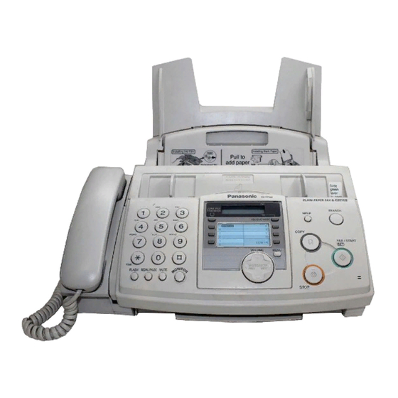
from the actual product. 3. INSTALLATION 3.1. LOCATION OF CONTROLS 3.1.1. FRONT VIEW (1) Handset (2) Document guides (3) Paper tray (4) Recording paper support (5) Recording paper entrance (6) Recording paper exit (7) Tension plate (8) Front cover (9) Document exit (10) Document entrance (11) Back cover open button (12) Back cover... -
Page 13: Control Panel
(1) Power inlet (2) Telephone line jack (3) External telephone jack (4) Speaker 3.1.3. CONTROL PANEL (1) [TONE] - To change from pulse to tone temporarily during dialing when your line has rotary pulse services. (2) One-touch keys - To use one-touch dial. - To transmit to multiple entries. - Page 14 (3) BROADCAST - To transmit a document to multiple parties. (4) [JUNK FAX PROHIBITOR] - To use junk fax prohibitor. (5) Display (6) [RECEIVE MODE] - To change the receiving mode. (7) [LOWER] - To select stations 6-10 for one-touch dial. (8) [HELP] - To print a quick reference.
- Page 15 - To mute your vice to the other party during a conversation. Press this button again to resume the conversation. (13) [MONITOR] - To initiate dialing without lifting the handset. (14) [NAVIGATOR, VOLUME] - To adjust volume. - To search for a stored name. - To select the features or feature settings during programming.
- Page 16 Caution: - When you operate this product, the power outlet should be near the product and easily accessible. - Be sure to use the telephone line cord included in this unit. - Do not extend the telephone line cord. Note: - To avoid malfunction, do not position fax machine near appliance such as TVs or speakers which generate an intense magnetic field.
-
Page 17: Installation Space
disturb the network condition of the device. 3.3. INSTALLATION 3.3.1. INSTALLATION SPACE The space required to install the unit is shown below. The dimensions given are necessary for the unit to operate efficiently. Note: - Avoid excessive heat or humidity. - Use the unit within the following ranges of temperature and humidity. -
Page 18: Installing The Paper Tray
- To protect the unit from damage, hold both sides when you move it. 3.3.2. INSTALLING THE PAPER TRAY To use A4 size paper Insert the tabs ( ) on the paper tray ( ) into the slots on the back of the unit. You need to install the A4 paper guide ( right side of he paper tray. - Page 19 Insert the recording paper support ( ) into the slot to the right of the recording paper exit ( ) , then into the left slot ( The recording paper will be ejectedfrom the top of the unit after printing. The recording paper support prevents the printed paper from curling.
- Page 20 Open the front cover ( ) by pulling up the center part ( 2 Release the back cover by pushing the green button ( ) on the right side of the unit. Release the back cover by pushingthe green lever ( ) in the unit.
- Page 21 Open the back cover ( 4 Insert the gear with the blue core of the front ink film roll ( ) into the left slot of the unit ( Insert the rear ink film roll ( The ink film is safe to touch,and will not rub off on your rands like carbon paper.
- Page 22 Turn the gear with the blue core ( ) in the direction of the arrow. Make sure that the ink film is wrapped around the blue core ) at least once.
-
Page 23: Installing The Recording Paper
First close the back cover securely ( ) by pushing down on the dotted area at both ends ).Then close the front cover securely ( 3.3.5. INSTALLING THE RECORDING PAPER Letter or A4 size recording paper can be loaded. The unit can hold up to 50 sheets of 75 g/m paper. - Page 24 2 Pull the tension plate forward ( ) and hold open The paper should not be over the tab ( while inserting the paper. If the paper is not inserted correctly, readjust the paper, paper may jam. 3.3.6. DOCUMENTS THE UNIT CAN FEED Note: - Remove chips, staples or other similar fasteners.
-
Page 25: Setting Your Logo
— Paper with printing on the opposite side that can be seen through the other side (i.e. newspaper) - Check that ink, paste or correction fluid has dried completely. - To transmit the document with a width of less than standard A4 size (210 mm), we recommend using a copy machine to copy the original document onto A4 or letter-sized paper, than transmit the copied document. - Page 26 3 Press [SET]. To correct a mistake Press [ ] or [ ] to move the cursor to incorrect character, and make the correction. 4 Enter your logo, up to 30 characters, using the dial keypad. Example: “BILL“ 1. Press [2] 2 times. To delete a character -Cursor ( ) will appear on the display.
- Page 27 To select characters using [+] or [-] Instead of pressing the dial keys, you can select characters using [+] or [-]. 1. Press [+] or [-] until the desired character is displayed. 2. Press [ ] to move the cursor to the next space. - The character displayed in step 1 is inserted.
-
Page 28: Maintenance Items And Component Locations
4. MAINTENANCE 4.1. MAINTENANCE ITEMS AND COMPONENT LOCATIONS 4.1.1. OUTLINE MAINTENANCE AND REPAIRS ARE PERFORMED USING THE FOLLOWING STEPS. 1. Periodic maintenance Inspect the equipment periodically and if necessary, clean any contaminated parts. 2. Check for breakdowns Look for problems and consider how they arose. If the equipment can be still used, perform copying, self testing or communication testing. - Page 29 4.1.2.1. MAINTENANCE LIST OPERATION CHECK REMARKS Document Path Remove any foreign matter such as paper. — Rollers If the roller is dirty, clean it with a damp Refer to DOCUMENT FEEDER cloth then dry thoroughly. Platen Roller If the platen is dirty, clean it with a damp —...
-
Page 30: Gear Operation
OPERATION CHECK REMARKS Abnormal, wear Replace the part. Check if the screws are — and tear or loose tight on all parts. parts 4.1.2.2. MAINTENANCE CYCLE Item Cleaning Replacement Cycle Cycle Procedure 1 Separation Roller (Ref. No. 141) 3 months 7 years* (31,500 Refer to HOW TO REMOVE... -
Page 31: Print Mode
4.2.1.2. PAPER PICK UP AND PAPER EXIT MODE The RX MOTOR rotate CCW and swing Gear B engages Gear C, and conveys its power to the Pickup Roller Gear. The Swing Gear B engages Gear D, and conveys its power to the Exit Roller Gear. Fig. -
Page 32: Copy Mode
4.2.1.4. COPY MODE RX side: Paper Pickup mode Print mode Paper Exit mode. TX side: Transmit mode. 4.3. JAMS 4.3.1. RECORDING PAPER JAMS When the recording paper has jammed in the unit The display will show the following. - Page 33 Open the front cover ( ) by pulling up the center part ( 2 Release the back cover by pushing the green button ( ) on the right side of the unit. Release the back cover by pushingthe green lever ( ) in the uniit.
- Page 34 Open the back cover ( Remove the jammed recording paper (...
- Page 35 Turn the gear with the blue core ( ) in the direction of the arrow. Make sure that the ink film is wrapped around the blue core ) at least once.
- Page 36 First close the back cover securely ( ) by pushing down on the dotted area at both ends ). Then close the front cover securely 7 Remove the recording paper and straighten. Pull the tension plate forward ( ) and hold open while inserting the paper.
- Page 37 Remove the recording paper and straighten. Pull the tension plate ( ) forward and hold open while inserting paper. Press [START] to clear the message. 4.3.2. DOCUMENT JAMS - SENDING...
- Page 38 Open the front cover ( ) by pulling up the center part ( Removethe jammed document carefully (...
- Page 39 Close the front cover securely ( Note: Do not pull out the jammed paper forcibly before opening the front cover. 4.4. CLEANING 4.4.1. DOCUMENT FEEDER If misfeeding occurs frequently or if smudges or black lines appear on a transmitted document or on the original of a copied document, clean the document feeder.
- Page 40 1 Disconnect the power cord and the telephone line cord. Open the front cover ( ) by pulling up the center part (...
- Page 41 Clean the document feeder rollers ( ) and rubber flap ( ) with a clothmoistened with isopropyl rubbing alcohol, and let all parts dry thoroughly. Clean the grass ( ) with a soft, dry cloth. Caution: Do not use paper products, such as paper towels or tissues.
-
Page 42: Thermal Head
Close the front cover securely ( 5 Connect the power cord and the telephone line cord. 4.4.2. THERMAL HEAD If smudges or black/white lines appear on a copied or received document, check whether there is dust on the thermal head and roller shaft, and clean the thermal head to remove the dust. 1 Disconnect the power cord and the telephone line cord. - Page 43 Open the front cover ( ) by pulling up the centre part ( 3 Release the back cover by pushing the green button ( ) on the right side of the unit. Release the back cover by pushingthe green lever ( ) in the unit.
- Page 44 Open the back cover ( Remove the ink film ( Clean the thermal head ( ) with a cloth moistened with isopropyl rubbing alcohol, and let it dry thoroughly. Caution: To prevent a malfunction due to static electricity, do not use a dry cloth and do not touch the thermal head directly.
-
Page 45: Disassembly Flow Chart
5.1. DISASSEMBLY FLOW CHART 5.1.1. UPPER CABINET SECTION... -
Page 46: Lower Cabinet Section
CROSS REFERENCE: A-1 : HOW TO REMOVE THE PAPER TRAY AND RECORDING PAPER SUPPORT A-2 : HOW TO REMOVE THE OPERATION PANEL BLOCK A-3 : HOW TO REMOVE THE OPERATION BOARD AND LCD A-4 : HOW TO REMOVE THE IMAGE SENSOR (CIS) A-5 : HOW TO REMOVE THE THERMAL HEAD A-6 :... -
Page 47: Disassembly Procedure
CROSS REFERENCE: A-1 : HOW TO REMOVE THE PAPER TRAY AND RECORDING PAPER SUPPORT B-1 : HOW TO REMOVE THE BOTTOM FRAME B-2 : HOW TO REMOVE THE DIGITAL, ANALOG, POWER SUPPLY, SENSOR BOARDS AND AC INLET B-3 : HOW TO REMOVE THE MOTOR BLOCK AND SEPARATION ROLLER B-4 : HOW TO REMOVE THE GEARS OF MOTOR BLOCK 5.2. -
Page 48: How To Remove The Operation Panel Block
5.2.2. HOW TO REMOVE THE OPERATION PANEL BLOCK... -
Page 49: How To Remove The Operation Board And Lcd
5.2.3. HOW TO REMOVE THE OPERATION BOARD AND LCD... -
Page 50: How To Remove The Image Sensor (Cis)
5.2.4. HOW TO REMOVE THE IMAGE SENSOR (CIS) -
Page 51: How To Remove The Thermal Head
5.2.5. HOW TO REMOVE THE THERMAL HEAD... - Page 52 5.2.6. HOW TO REMOVE THE PLATEN ROLLER AND BACK COVER...
-
Page 53: How To Remove The Pickup Roller
5.2.7. HOW TO REMOVE THE PICKUP ROLLER... - Page 54 5.2.8. HOW TO REMOVE THE CASSETTE LEVER...
-
Page 55: How To Remove The Bottom Frame
5.2.9. HOW TO REMOVE THE BOTTOM FRAME... - Page 56 5.2.10. HOW TO REMOVE THE DIGITAL, ANALOG, POWER SUPPLY, SENSOR BOARDS AND AC INLET...
- Page 57 5.2.11. HOW TO REMOVE THE MOTOR BLOCK AND SEPARATION ROLLER...
- Page 58 5.2.12. HOW TO REMOVE THE GEARS OF MOTOR BLOCK...
-
Page 59: Installation Position Of The Lead Wires
5.3. INSTALLATION POSITION OF THE LEAD WIRES... -
Page 60: Troubleshooting Guide
6. TROUBLESHOOTING GUIDE 6.1. USER RECOVERABLE ERRORS If the unit detects a problem, one or more of the following messages will appear on the display. The explanations given in the [ ] are for servicemen only. - There is something wrong with the unit. -
Page 61: Document Feeder
- The document was not fed into the unit properly. Reinsert the document. If misfeeding occurs frequently, clean the document feeder rollers and try again. (Refer to DOCUMENT FEEDER ().) - Attempted to transmit a document longer than 600 mm. Press the [STOP] to remove the document. -
Page 62: Installing The Ink Film
- There is no space to store new entries in navigator directory. Erase unnecessary entries. - The unit has a document in memory. See the other displayed message instructions to print out the document. - The memory is full of received documents due to lack of recording paper or a recording paper jam. - Page 63 - The other party´s fax machine is busy or has run out of recording paper. Try again. - The ink film is empty. Replace the ink film with a new one. - The ink film is not installed. Install it. Refer to INSTALLING THE INK FILM - The ink film is slack.
-
Page 64: Document Jams - Sending
- The document is jammed. Remove the jammed document. (Refer to DOCUMENT JAMS - SENDING ().) - A transmission error occurred. Try again. - The unit is too hot. Let the unit cool down. 6.2. PROGRAMMING AND LISTS The programming functions are used to program the various features and functions of the machine, and to test the machine. - Page 65 6.2.3. SERVICE FUNCTION TABLE Code Function Set Value Effective Default Remarks Range Pause time set X 100 001~600 ---------- msec Flash time X 10 ms 01~99 ---------- Dial speed select 1, 2 ---------- 1: 10 pps 2: 20 pps Belldetectiontime X100msec ---------- CED frequency select...
- Page 66 Code Function Set Value Effective Default Remarks Range Receive equalizer select When the telephone station is 1: 0 km from the unit or reception cannot 2: 1.8 km performed correctly, adjust 3: 3.6 km accordingly. 4: 7.2 km Transmission equalizer When the telephone station is 1: 0 km select...
- Page 67 Code Function Set Value Effective Default Remarks Range Time between CED and 1:75 msec See Symptom/Countermeasure 300bps for long distance and international 2:500 calls in THE UNIT CAN COPY, msec CANNOT EITHER TRANSMIT 3:1 sec RECEIVE LONG DISTANCEOR INTERNATIONL COMMUNICATIONS Refer to RECEIVE PROBLEM THE UNIT CAN COPY, BUT...
-
Page 68: Test Functions
Code Function Set Value Effective Default Remarks Range Receive speed selection 1:9600BPS Adjusts the speed to start training during FAX reception. Refer RECEIVE PROBLEM () and THEUNIT 2:7200BPS CAN COPY, BUT THE TRANSMISSION AND RECEPTION IMAGE ARE 3:4800BPS INCORRECT(). 4:2400BPS Redial tone detect 1:ON 2: 1, 2... - Page 69 Test Mode Type of Code Function Mode Operation after code input MOTOR TEST Service “5” “5” “6” Rotates the transmission and reception motor to check Mode operation of the motor. START 12: Document feed 24: Recording paper is fed Press [STOP] button to quit. MODEM TEST Service “5”...
-
Page 70: Dtmf Single Tone Transmit Selection
Test Mode Type of Code Function Mode Operation after code input SENSOR Service “8” “1” “5” If you enter this mode and operate sensor levers with CHECK & VOX Mode hands, the LCD display of the related sensor (or switch) START CHECK turns ON / OFF. -
Page 71: Button Code Table
High Frequency Low Frequency (Hz) (Hz) “1” “5” 1209 “2” “6” 1336 “3” “7” 1477 “4” “8” 1633 When set to OFF (=2), the 12 keys and transmission frequencies are as shown. High (Hz) 1209 1336 1477 Low (Hz) “1” “2”... - Page 72 2. Left margin / Top margin 3. Thermal head 1 dot...
-
Page 73: Remote Programming
4. Use this test pattern to confirm the torque limiter for ink film and platen roller timing 6.4. REMOTE PROGRAMMING If, after the call is connected, the customer describes the situation and it is determined that the problem can be corrected by making parameter changes, this function makes it possible to change parameters such as the user codeand service code from another fax (using DTMF tones). - Page 74 Therefore, travel to the customer's location is not required. However, it is not possible to change all the parameters remotely (PROGRAM MODE TABLE ()). The function used to accomplish this is remote programming. First, in order to check the current status of the service code parameter, print out the setup list (code: 991) and the service list (code: 999) from the customer's fax machine.
-
Page 75: Program Mode Table
CROSS REFERENCE: PROGRAM MODE TABLE() 6.4.2. PROGRAM MODE TABLE... - Page 76 Code Function Set Value Default Set date and time mm/dd/yy hh:mm Jan/01/2002 Your logo --------- None Your FAX number --------- None Print sending mode 1:ERROR/ 2:ON / 3:OFF ERROR FAX ring count 1 to 5 rings (for ext. tam) Remote TAM activation ON / OFF OFF / ID=11 Dialing mode...
- Page 77 Code Function Set Value Default Document jam detection 1:ON / 2:OFF Key test --------- --------- Break % select 1:61% / 2:67% ITS auto redial time set 00~99 ITS auto redial line disconnection time 001~999sec 065sec Remote turn-on ring number 01~99 FAX auto redial time set 00~99 FAX auto redial line disconnection time...
-
Page 78: The Example Of The Printed List
Example: If you want to set value in the "004 Transmission report mode", press the dial key number 1,2 or 3 corresponding to the Set Value you want to select. (1:ERROR/2:ON/3:OFF) 6.5. THE EXAMPLE OF THE PRINTED LIST 6.5.1. USER MODE Note: The above values are the default values. - Page 79 Note: The above values are the default values. 6.5.3. HISTORY...
- Page 80 Note: See the following descriptions of this report. Item No. (1) ~ (44) are corresponding to the listed items in DESCRIPTIONS OF THE HISTORY REPORT(). 6.5.3.1. DESCRIPTIONS OF THE HISTORY REPORT (1) ROM VERSION FLASH ROM version (2) SUM FLASH ROM internal data calculation.
- Page 81 (3) YOUR LOGO The user logo recorded in the unit. If it is not recorded, NONE will be displayed. (4) YOUR TELEPHONE NUMBER The user telephone number recorded in the unit. If it is not recorded, NONE will be displayed. (5) FAX PAGER NUMBER If you program a pager number into the unit, the pager number will be displayed here.
-
Page 82: Troubleshooting Details
(32) NUMBER OF DIVIDED PRINTING IN FAX RECEPTION The number of faxes received that were divided into more than one sheet since the unit was purchased. (33) Not Used (34) FAX MODE Means the unit received a fax message in the FAX mode. (35) MAN RCV Means the unit received a fax message by manual operation. -
Page 83: Troubleshooting Items Table
CROSS REFERENCE: USER RECOVERABLE ERRORS SIMPLE CHECK LIST DIGITAL BOARD SECTION() POWER SUPPLY BOARD SECTION 6.6.3. TROUBLESHOOTING ITEMS TABLE... - Page 84 ITEM SYMPTOM REFERENCE The document does not feed. NO DOCUMENT FEED (Auto Document Feeder) Document jam DOCUMENT JAM Multiple feed MULTIPLE FEED Skew SKEW Recording paper feed The recording paper does not feed. THE RECORDING PAPER DOES NOT Paper jam PAPER JAM Multiple feed and skew MULTIPLE FEED AND SKEW...
- Page 85 SERIAL NO. DATE FUNCTION JUDGEMENT REFERENCE FAX operation Transmission OK / NG Receiving OK / NG Copy operation OK / NG Telephone Handset transceiver / OK / NG operation receiver MONITOR sound OK / NG Ringer sound OK / NG Dial operation OK / NG Volume operation...
-
Page 86: Document Jam
CROSS REFERENCE: TEST FUNCTIONS DIGITAL BOARD SECTION() POWER SUPPLY BOARD SECTION SENSOR SECTION STEPPING MOTOR DRIVE CIRCUIT (TX) HOW TO REMOVE THE MOTOR BLOCK AND SEPARATION ROLLER HOW TO REMOVE THE GEARS OF MOTOR BLOCK 6.6.4.2. DOCUMENT JAM... - Page 87 CROSS REFERENCE: TEST FUNCTIONS SENSOR SECTION DISASSEMBLY INSTRUCTIONS 6.6.4.3. MULTIPLE FEED - When using thick paper etc., sometimes the document will not be fed.
- Page 88 Fig. B...
- Page 89 CROSS REFERENCE: DOCUMENT FEEDER() DISASSEMBLY INSTRUCTIONS HOW TO REMOVE THE MOTOR BLOCK AND SEPARATION ROLLER Note: When confirming if the characters are extended or distorted, or if the feed problem is occurred, use this test chart format...
- Page 90 (Fig. B). 6.6.4.4. SKEW * We recommend making a copy of the Fig. B document in MULTIPLE FEED () and using it. CROSS REFERENCE: COMPONENT LOCATIONS DISASSEMBLY INSTRUCTIONS() 6.6.4.5. THE RECORDING PAPER DOES NOT FEED...
-
Page 91: Paper Jam
* We recommend making a copy of the Fig. B document in MULTIPLE FEED ()and using it. CROSS REFERENCE: INSTALLING THE RECORDING PAPER() TEST FUNCTIONS HOW TO REMOVE THE PICKUP ROLLER HOW TO REMOVE THE GEARS OF MOTOR BLOCK DIGITAL BOARD SECTION() POWER SUPPLY BOARD SECTION SENSOR SECTION... - Page 92 CROSS REFERENCE: DISASSEMBLY INSTRUCTIONS HOW TO REMOVE THE PICKUP ROLLER TEST FUNCTIONS SENSOR SECTION SENSORS AND SWITCHES 6.6.4.7. MULTIPLE FEED AND SKEW CROSS REFERENCE: HOW TO REMOVE THE PICKUP ROLLER OPERATION PANEL SECTION...
- Page 93 6.6.4.8. THE SENT FAX DATA IS SKEWED * We recommend making a copy of the Fig. B document in MULTIPLE FEED() and using it. CROSS REFERENCE: SKEW() 6.6.4.9. THE RECEIVED FAX DATA IS SKEWED * We recommend making a copy of the Fig. B document in MULTIPLE FEED() and using it.
- Page 94 6.6.4.10. RECEIVED OR COPIED DATA IS EXPANDED * We recommend making a copy of the Fig. B document in MULTIPLE FEED() and using it. CROSS REFERENCE: DOCUMENT FEEDER HOW TO REMOVE THE MOTOR BLOCK AND SEPARATION ROLLER 6.6.4.11. A BLANK PAGE IS COPIED...
- Page 95 * We recommend making a copy of the Fig. B document in MULTIPLE FEED () and using it. CROSS REFERENCE: HOW TO REMOVE THE THERMAL HEAD() TEST FUNCTIONS A BLANK PAGE IS RECEIVED THERMAL HEAD()
- Page 96 6.6.4.12. A BLANK PAGE IS RECEIVED...
- Page 97 CROSS REFERENCE: TEST FUNCTIONS() A BLANK PAGE IS COPIED() ANALOG BOARD SECTION() 6.6.4.13. BLACK OR WHITE VERTICAL LINE...
- Page 98 * We recommend making a copy of the Fig. B document in MULTIPLE FEED () and using it. CROSS REFERENCE: THERMAL HEAD HOW TO REMOVE THE THERMAL HEAD 6.6.4.14. BLACK OR WHITE LATERAL LINE ON PRINT OUT...
- Page 99 * We recommend making a copy of the Fig. B document in MULTIPLE FEED() and using it. CROSS REFERENCE: DISASSEMBLY INSTRUCTIONS() TEST FUNCTIONS() A BLANK PAGE IS COPIED() DIGITAL BOARD SECTION() 6.6.4.15. AN ABNORMAL IMAGE IS PRINTED...
-
Page 100: Communication Section
* We recommend making a copy of the Fig. B document in MULTIPLE FEED () and using it. CROSS REFERENCE: HOW TO REMOVE THE THERMAL HEAD TEST FUNCTIONS() ANALOG BOARD SECTION() 6.6.5. COMMUNICATION SECTION Find the problem in the table shown below, and refer to the corresponding troubleshooting procedure in DEFECTIVE FACSIMILE SECTION ( ). -
Page 101: Troubleshooting
Symptom Content Possible cause Troubleshooting Problem with the feeding The paper is not fed properly when faxing. mechanism. (Nor in the copy mode.) Troubleshooting Problem with the service The fax usually transmits successfully but line or with the sometimes fails. (The unit can copy receiver's fax. - Page 102 CROSS REFERENCE: DOCUMENT FEEDER() HOW TO REMOVE THE MOTOR BLOCK AND SEPARATION ROLLER ADF (Auto Document Feed) SECTION() OPERATION PANEL SECTION() 6.6.5.1.2. SOMETIME THERE IS A TRANSMIT PROBLEM...
- Page 103 Note: "596: Transmit level set" represents a service code. (Refer to SERVICE FUNCTION TABLE ().) 6.6.5.1.3. RECEIVE PROBLEM First confirm whether the recording paper is installed properly or not before starting troubleshooting. (Refer to "Remarks".)
- Page 104 Note: "596: Transmit level set" represents a service code. (Refer to SERVICE FUNCTION TABLE ().) Remarks: Regarding the reception problem, we have investigated the conceivable causes in the flow chart except for the software-related errors. However, some troubles may occur due to the software- related problems such as "OUT OF PAPER"...
- Page 105 PAPER JAMMED CHECK FILM Please refer to USER RECOVERABLE ERRORS () for the above items. If it turns out to be a hardware deformity, please check each sensor. (Refer to TEST FUNCTIONS ().) 6.6.5.1.4. THE UNIT CAN COPY, BUT CANNOT TRANSMIT/RECEIVE CROSS REFERENCE: TEST FUNCTIONS()
- Page 106 (Cause and Countermeasure) As shown in the chart above, the total handshaking time must be reduced, but because of the long distance connection and linking of several stations, the line connection time cannot be reduced. Accordingly, the following countermeasures should betried. (A)...
- Page 107 No. Countermeasure Echo Communication Problem Countermeasure Service Side Example 1 Sending side Some time is needed to Add a dummy signal to the Service code compare the level of the beginning of the training (International receiving and sending signals signal. select) for the echo canceler.
- Page 108 Fig. b (Countermeasure by Changing the CED Frequency) Fig. c (Countermeasure by Changing the Interval Between CED and DIS) Fig. d (Countermeasure by Ignoring the 1st DIS)
- Page 109 <TX side signal> <RX side signal> <Countermeasure> 2nd / 3rd DCS / Training & delayed CFR / FTT at TX side & delayed MCF / PIP / PIN / RTP / 2nd / 3rd EOP / EOM / MPS at TX side delayed DCS &...
- Page 110 - Refer to SERVICE FUNCTION TABLE(). 6.6.5.1.7. HOW TO RECORD FAX SIGNAL BY USING PC Recording FAX signal is one of the useful analysis measures to solve communication problems. The way of recording easily by using PC is shown as follows. 1.
- Page 111 4. PC setting and recording 1. Set LINE IN to be valid in the volume control setting. Refer to the PC instruction book. 2. Start up the PC software “ SOUND RECORDER”. (This software is bundled to Windows OS, which can create WAV file.) Set the audio format “...
- Page 112 (2) RESULT (3) MODE SYMPTOM CODE PRESSED THE STOP KEY SND & Communication was interrupted by the STOP button. DOCUMENT JAMMED The document paper is jammed. NO DOCUMENT No document paper. OTHER FAX NOT Transmission is finished when the T1 TIMER RESPONDING expires.
- Page 113 SERVICE FUNCTION TABLE ().) Note*: If the problem remains, see the following "Countermeasure" flow chart.
- Page 114 CROSS REFERENCE: TEST FUNCTIONS...
- Page 115 CROSS REFERENCE: TEST FUNCTIONS...
- Page 116 CROSS REFERENCE: TEST FUNCTIONS...
- Page 117 CROSS REFERENCE: TEST FUNCTIONS()
-
Page 121: Special Service Journal Reports
CROSS REFERENCE: TEST FUNCTIONS 6.6.6. SPECIAL SERVICE JOURNAL REPORTS Journal 2 and Journal 3 shown below, which are special journals giving the additional detailed information about the latest 35 communications, can be printed by Service Code 881 or 882. Remote printing function for the journalreports (JOURNAL, JOURNAL 2 and JOURNAL 3) is also available for service technicians. - Page 122 provide different information on the same item (communication). HOW TO READ JOURNAL REPORTS: Example: 1. Look at NO. 01 in the JOURNAL. If you want to know about the details about that item, see NO. 01 in the JOURNAL 2 and the JOURNAL 3.
- Page 123 6.6.6.1. JOURNAL 2 Refer to JOURNAL 2 in PRINTOUT EXAMPLE(). Journal 2 displays the additional detailed information about the last 35 communications. Descriptions: (1) RCV. MODE Indicates which receive mode the unit was in when the unit received a fax message. This information is also displayed when the unit transmitted a fax message.
- Page 124 communications terminated by "No Response". (Some of the communications terminated by "No Response" were not displayed in the JOURNAL.) When a fax transmission cannot be performed because the other party’s unit is set to the TEL mode, "No response" will be printed. 6.6.6.2.
-
Page 126: Digital Board Section
6.6.7. DIGITAL BOARD SECTION When the unit fails to boot up the system, take the troubleshooting procedures very carefully. It may have a serious problem. The symptom: No response when the power is turned on. (No LCD display, and keys are not accepted.) The first step is to check the power source. - Page 127 Note: 1. Electrical continuity may have existed at the factory check, but a faulty contact occurred as a result of vibration, etc., during transport. 2. Solder waste remaining on the board may get caught under the IC during transport, causing a short circuit. Before we begin mass production, several hundred trial units are produced at the plant, various tests are applied and any malfunctions are analyzed.
- Page 128 Between the DRAM (IC503), Gate Array IC (IC520) signal lines are controlled by voltages of 5V (H) or 0V (L). Digital Block Diagram You also need to check the signal lines listed here [List 1] when the unit fails to boot up the system.
- Page 129 Normal Wave Patterns Remarks: When you use an oscilloscope to judge whether a signal to be tested is normal or NG, perform the signal check in exactly the same order as in [List 1]. (If the ASIC fails to access the FLASH ROM, the ASIC cannot access DRAM normally.) The digital circuit actually operates according to the timing combinations of these signals.
- Page 130 6.6.7.1. CHECK THE STATUS OF THE DIGITAL BOARD...
-
Page 131: Initializing Error
CROSS REFERENCE: NG Wave pattern (Refer to NG EXAMPLE) 6.6.7.2. INITIALIZING ERROR After the power is turned on, the ASIC initializes and checks each IC. The ROM, DRAM, and modem are checked. If initialization fails for the ICs, the system will not boot up. In this case, please find the cause as follows. - Page 132 CROSS REFERENCE: NG EXAMPLE CHECK THE STATUS OF THE DIGITAL BOARD() POWER SUPPLY BOARD SECTION...
- Page 133 CROSS REFERENCE: CHECK THE STATUS OF THE DIGITAL BOARD() Other NG example while the power is ON and the LCD displays the following. 6.6.7.3. NG EXAMPLE...
-
Page 134: Analog Board Section
6.6.8. ANALOG BOARD SECTION This chapter provides the testing procedures required for the analog parts. A signal route to be tested is determined depending upon purposes. For example, the handset TX route begins at the handset microphone and the signalis output to the telephone line. The signal mainly flowing on this route is analog. - Page 135 Note: { }: Inside the digital board 6.6.8.2. DEFECTIVE ITS (Integrated Telephone System) SECTION 1. No handset transmission / reception and no monitor reception Perform a signal test in the ITS or the NCU section and locate a defective point (where the signal disappears) on each route between the handset microphone and telephone line (sending), or between the telephone line and the handset speaker (receiving),or between the microphone and the telephone line (sending), or...
- Page 136 3. No ring tone (or No bell) CROSS REFERENCE: CHECK SHEET()
- Page 137 SECTION() 4. No tone dialing CROSS REFERENCE: CHECK SHEET() 6.6.8.3. DETECTIVE TAM INTERFACE SECTION 1. The FAX turns on, but does not arrive through TAM. CROSS REFERENCE:...
- Page 138 CIRCUIT OPERATION() 2. A FAX is received, but won't switch from TAM to FAX. CROSS REFERENCE: ANALOG BOARD SECTION() TAM INTERFACE SECTION() 6.6.9. POWER SUPPLY BOARD SECTION 6.6.9.1. KEY COMPONENTS FOR TROUBLESHOOTING Check the following parts first: F101, D101-D104, C106, Q101, PC101 and IC101. This comes from our experience with experimental tests.
-
Page 139: Troubleshooting Flowchart
6.6.9.2. TROUBLESHOOTING FLOW CHART... - Page 142 6.6.9.3. BROKEN PARTS REPAIR DETAILS (D101, D102, D103, D104) Check for a short-circuit in terminal 4. If D101, D102, D103 and D104 are short-circuits, F101 will melt (open). In this case, replace all of the parts (D101, D102, D103, D104, F101). (Q101) The worst case of Q101 is a short-circuit between the Drain and Gate because damage expands to the peripheral circuit of Q101.
-
Page 143: Sensor Section
6.6.10.2. NO LCD INDICATION CROSS REFERENCE: TEST FUNCTIONS 6.6.11. SENSOR SECTION Refer to SENSORS AND SWITCHES() for the circuit descriptions. The Test Function makes the sensor circuit check easier. (Refer to TEST FUNCTIONS().) For example, as for "COVER OPEN SENSOR", "CO" is turned ON/OFF on the display when you open or close the front cover. -
Page 144: Cis (Contact Image Sensor) Section
6.6.11.3. CHECK THE COVER OPEN (SW502)...."COVER OPEN " 6.6.11.4. CHECK THE HOOK SWITCH (SW101) 6.6.11.5. CHECK THE PAPER TOP SENSER (PS501)......"PAPER JAMMED" 6.6.11.6. CHECK THE FILM SENSER (SW501)......"CHECK FILM SLACK" 6.6.12. CIS (Contact Image Sensor) SECTION Refer to SCANNING BLOCK(). -
Page 145: Thermal Head Section
CROSS REFERENCE: TEST FUNCTIONS 6.6.13. THERMAL HEAD SECTION Refer to THERMAL HEAD(). -
Page 146: Circuit Operations
7. CIRCUIT OPERATIONS 7.1. CONNECTION DIAGRAM... -
Page 147: General Block Diagram
7.2. GENERAL BLOCK DIAGRAM The following is an outline of each device IC on the digital board. (Refer to GENERAL BLOCK DIAGRAM().). 1. ASIC (IC501) Composed mainly of an address decoder and a modem control. Controls the general FAX operations. Controls the operation panel I/F. - Page 148 CPU and Real time clock 2. Flash ROM (IC523) Contains all of the program instructions on the unit operations. This memory is used mainly for the parameter working in the storage area. 3. Dynamic RAM (IC503) This memory is used mainly for the parameter working in the storage area.
-
Page 149: Control Section
7.3. CONTROL SECTION 7.3.1. BLOCK DIAGRAM 7.3.2. MEMORY MAP... - Page 150 7.3.3. ASIC (IC501) This custom IC is used for the general FAX operations.
-
Page 151: Analog Unit
1. CPU: This model uses a Z80 equivalent to the CPU operating at 12 MHz. Most of the peripheral functions are performed by custom- designed LSIs. Therefore, the CPU only works for processing the results. 2. RTC: Real Time Clock 3. - Page 153 Note*: This memory is incorporated into the ASIC (IC501) and used for the image processing. Fig. A shows the memory map of the Image Data RAM. 7.3.4. FLASH MEMORY (IC523) The 512KB ROM (FLASH MEMORY) carries a common area of 32KB and bank areas which each have 8KB (BK4~BK63).
- Page 154 SIGNAL POWER DESCRIPTION SUPPLIED VOLTAGE 3.3V INPUT PORT (PTOP) 3.3V INPUT PORT (REED) IRDATXD/IOP 3.3V OUTPUT PORT (CISLED) IRDARXD/IOP80 3.3V INPUT PORT (DSR) TXD/IOP 3.3V INPUT PORT (TXD) RXD/IOP 3.3V OUTPUT PORT (SENLED1) XRTS/IOP 3.3V INPUT PORT (HOOK) XCTS/IOP 3.3V OUTPUT PORT (SPMUTE) VDD (2.5V) 3.3V...
- Page 155 SIGNAL POWER DESCRIPTION SUPPLIED VOLTAGE XMDMINT 3.3V MODEM INTERRUPT XMDMCS 3.3V MODEM CHIP SELECT XRAS/IOP 3.3V DRAM (IC503) ROW ADDRESS STROBE XCAS1/IOP 3.3V DRAM (IC503) CULUM ADDRESS STROBE XCAS2/IOP 3.3V DRAM(IC503) CHIPSELECT XRESCS2 3.3V GATE ARRAY CHIP SELECT 3.3V CPU DATA BUS 3 3.3V CPU DATA BUS 2 3.3V...
- Page 156 SIGNAL POWER DESCRIPTION SUPPLIED VOLTAGE RBA5 3.3V ROM/RAM BANK ADDRESS 5 RBA6/IOP96 3.3V STB1 3.3V STROBE SIGNAL OUTPUT TO THERMAL HEAD STB2 3.3V STROBE SIGNAL OUTPUT TO THERMAL HEAD STB3 3.3V NOT USED XRESET 3.3V RESET INPUT VDD (3.3V) ----- POWER SOURCE (+3.3V) POWER SOURCE (GND) POWER SOURCE (GND)
- Page 157 SIGNAL POWER DESCRIPTION SUPPLIED VOLTAGE VDDA (2.5V) 3.3V POWER SOURCE (ANALOG +2.5V) VREFB 2.5V A/D CONVERTER'S ZERO STANDARD VOLTAGE OUTPUT 3.3V ANALOG PART STANDARD VOLTAGE SIGNAL VREFT 3.3V A/D CONVERTER'S FULL SCALE VOLTAGE OUTPUT VSSA POWER SOURCE (ANALOG GND) 7.3.6. RESET CIRCUIT (WATCH DOG TIMER) The output signal (reset) from pin 4 of the voltage detect IC (IC507) is input to the ASIC (IC501) 114 and 106 pins.
-
Page 158: Rtc Backup Circuit
becomes low level. The terminal of the 'WDERR' signal is connected to the reset line, so the 'WDERR' signal works as the reset signal. 7.3.7. RTC BACKUP CIRCUIT 1. Function This unit has a lithium battery (BAT501) which works for Real Time Clock IC (RTC: inside IC501). -
Page 159: Supervision Circuit For The Thermal Head Temperature
7.3.8. SUPERVISION CIRCUIT FOR THE THERMAL HEAD TEMPERATURE 1. Function The thermistor changes the resistor according to the temperature and uses the thermistor's characteristics. The output of pin 137 of IC501 becomes a low level. Then when it becomes a high level, it triggers point A In point C, accordingto the voltage output time, the thermal head's temperature is detected. -
Page 160: Facsimile Section
7.4. FACSIMILE SECTION 7.4.1. IMAGE DATA FLOW DURING FACSIMILE OPERATION Copy (Fine, Super-Fine, Half Tone) 1. Line information is read by CIS (to be used as the reference white level) via route1, and is input to IC501. Refer to BLOCK DIAGRAM() 2. - Page 161 image processing, white is regarded as"0" and black is regarded as "1". Then via routes4 and 5, they are stored in RAM. 4. The white/black data stored as above via routes6 and 8 is input to the P/S converter. The white/black data converted to serial data in the P/S converter is input to the Thermal Head via route9 and is printedout on recording paper.
-
Page 162: Block Diagram
7.4.2. BLOCK DIAGRAM 7.4.3. THERMAL HEAD 1. Function This unit utilizes the state of the art thermal printer technology. The ink film is chemically processed. The ink film is comprised of two parts: an ink layer and a base film. When the thermalhead contacts this ink film, it emits heat momentarily, and the ink layer is melted and transferred to the paper. - Page 163 the original document is reproduced. 2. Circuit Operation Refer to the block diagram and the timing chart on the following page. There are 9 driver ICs aligned horizontally on the thermal head and each one of these ICs can drive 192 heat-emitting registers. This means that one line is at a density of 192×9=1728 dots=(8 dots/mm).
- Page 164 [Print speed of one-line: 4.608msec] (ii) Print Duty more than 50% The sequence is shown on TIMING CHART When print duty is more than 50%, IC520 pin 45 (NEWSTB1) and IC501 pin 103 (STB1) are the same signal. [IC520 pin 44 (NEWSTB2) and IC501 pin 104 (STB2) are the same signal.] [Print speed of one-line: 4.608msec x 2 = 9.216msec] TIMING CHART (i) Print Duty 50% or less...
-
Page 165: Scanning Block
(ii) Print Duty more than 50% 7.4.4. SCANNING BLOCK The scanning block of this device consists of a control circuit and a contact image sensor made up of a celfoc lens array, an LED array, and photoelectric conversion elements. - Page 166 When an original document is inserted and the start button pressed, pin 21 of IC501 goes to a high level and the transistor Q507 turns on.This applies voltage to the LED array to light it. The contact image sensor is driven by each of the FTG-F1signals output from IC501, and the original image illuminated by the LED array undergoes photoelectric conversion to output an analog image signal (SIG).
- Page 167 Stepping Motor Drive Mode Function Mode Phase Speed Pattern Copy Fine or 432 pps (t=1/ photo 432) Super Fine 216 pps (t=1/ 216) Paper ——— 432 pps (t=1/ Feed 432) Stand-by ——— None All phases currently off. The motor suspends while it is in the receive mode (about 70~80 msec), pin 131 of ASIC IC501...
- Page 168 becomes a low level and Q507 turns OFF. Then Q504 also turns OFF, and instead of +24 V, +5 V is supplied through D504 so that the motoris held in place. When the system is in the stand-by mode, all of the motor drive transistors turn OFF. Consequently, the motor current stops. 7.4.6.
-
Page 169: Gear Section
Function Mode Phase Speed Pattern Copy Fine or 432 pps (t=1/ photo 432) Super Fine 216 pps (t=1/ 216) Paper ——— 432 pps (t=1/ Feed 432) Stand-by ——— None All phases currently off. The motor suspends while it is in the receive mode (about 70~80 msec), pin 124 of ASIC IC501 becomes a low level and Q503 turns OFF. - Page 170 Sensor Sensor or Switch Message Error Sensor Circuit Name Location Operation SW353 Document set SW [CHECK DOCUMENT] Panel SW352 [REMOVE DOCUMENT] Document top SW Digital PCB PS501 Paper Top [PAPER JAMMED] Analog P.C.B SW101 Hook ———— Sensor P.C.B SW501 Film Detection [CHECK FILM SLACK] SW502 [COVER OPEN]...
- Page 171 7.6.2. DOCUMENT SET SW (SW353)...."CHECK DOCUMENT" When a document is set, the SW turns ON, and the input signal of IC301-9 pin (Operation) becomes a low level. When there is no document, the SW turns ON, and the input signal of IC301- 9 pin (Operation) becomes a high level.
-
Page 172: Modem Section
low. Digital Board Signal (IC501-25 pin) ON-Hook Low level OFF-Hook High level 7.6.5. PAPER TOP SENSOR (PS501)......"PAPER JAMMED" When the recording paper is loaded on the print head, the shelter plate shuts the sensor light, and the photo transistor turns OFF. The input signal of IC501-19 pin becomes a high level. Usually, the shelter plate is lifted, the photo transistorturns ON, and the input signal of IC501-19 pin becomes a low level. - Page 173 are demodulated and converted into digital image signals. The communication format and procedures for FAX communication are standardized by ITU-T. This1 chip modem (IC505) has hardware which sends and detects all of the necessary signals for FAX communication. It can be controlled by writing commands from the CPU (IC501: inside ASIC) to the register in the modem (IC505).
- Page 174 to include integrated services. 3. Facsimile Call Time Series Facsimile Call Time Series As shown in the following diagram, the facsimile call time series is divided into five phases. Phase A : Call setting Call setting can be manual/automatic. Phase B : Pre-message procedure Phase B is a pre-processing procedure and sequence for confirming the status of the terminal, transmission route, etc., and for terminal control.
- Page 175 5. Facsimile Standards Telephone Network Facsimile G3 Machine Item Connection Control Mode Telephone Network Signal Mode Terminal Control Mode T. 30 Binary Facsimile Signal Format Digital Modulation Mode PSK (V. 27 ter) or QAM (V. 29) Transmission Speed 300 bps (Control Signal) 2400, 4800, 7200, 9600 bps (FAX Signal) Redundancy Compression 1 dimension : MH Mode...
- Page 176 Control signals are comprised mainly of 8-bit identification signals and the data signals added to them. Data signals are added to DIS and DCS signals. Signal..DIS (Digital Identification Signal) Identification Signal Format..00000001 Function: Notifies the capacity of the receiving unit. The added data signals are as follows. Signal..DCS (Digital Command Signal) Identification Signal Format..X1000001 Example (Some models do not support the following items.):...
- Page 177 Bit No. DIS/DTC 17, 18 Recording width capabilities Recording width (0, 0) 1728 picture elements along scan line 1728 picture elements along scan line length of length of 215 mm ± 1% 215 mm ± 1% (0, 1) 1728 picture elements along scan line 2432 picture elements along scan line length of length of...
- Page 178 Bit No. DIS/DTC Validity of bits 17, 18 Recording width Bits 17, 18 are valid Recording width indicated by bits 17, Bits 17, 18 are invalid Recording width indicated by this field information Recording width capability 1216 picture Middle 1216 elements of 1728 picture elements along scan line length of 151 ±...
- Page 179 Signal Identification Signal Format Function Training 1 ——————— A fixed pattern is transmitted to the receiving speed (2400 to 9600 bps) designated by DCS, receiving side optimizes the automatic equalizer, according to this signal. ——————— Sends 0 continuously for 1.5 seconds at the same speed as the training signal.
-
Page 180: Modem Circuit Operation
7.7.2. MODEM CIRCUIT OPERATION The modem (IC505) has all the hardware satisfying the ITU-T standards mentioned previously. When the ASIC IC501 (61) is brought to a low level, the modem (IC505) is chip-selected and the resistors inside IC are selected by the select signals from ASIC (IC501) ADR0-ADR4 (pin 81~85). Commands are written through the data bus, and all processingis controlled by the ASIC (IC501) according to ITU-T procedures. -
Page 181: Analog Section
units. Here, the internal equalizer circuit reduces the image signals to a long-distance receiving level. This is designed to correct the characteristics of the frequency band centered around 3 kHz and maintain a constant receiving sensitivity. It can be set in the service mode. Refer to CHECK SHEET(). -
Page 182: Ncu Section
placed into the TX system. 7.8.1. ANALOG UNIT BLOCK DIAGRAM 7.9. NCU SECTION 7.9.1. GENERAL This section is the interface between the telephone line and external telephone. It is composed of an EXT. TEL line relay (RLY101), bell detection circuit, pulse dial circuit, TAM interface circuit, line amplifier and sidetone circuits and a multiplexer. -
Page 183: Line Amplifier And Side Tone Circuit
controlled by pin (138) of IC501, makes the pulsedial operation possible. IC501 (138) LINE RLY Low Level CN517 (12) CN101 (12) Q102 OFF RLY101 OFF : DC Loop OFF IC501 (138) LINE RLY High Level CN517 (12) CN101 (12) Q102 ON RLY101 ON : DC Loop ON 7.9.6. - Page 184 Keying) format. Data "0" is a 1200 Hz sine wave, and data 1 a 2200 Hz sine wave. There are two type of the message format which can be received: i.e.the single data message format and multiple data message format. The multiple data format allows to transmit the name and data code information in addition to the time and telephone number data.
- Page 185 7.10. ITS (Integrated Telephone System) AND MONITOR SECTION 7.10.1. GENERAL During the monitor operation, the speaker output passes through the power amplifier (IC102) [Analog board]. The DTMF signal is output from the modem (IC505: digital board). The alarm tone, the key tone, bell tone, and beep are output from gate array IC501 (digital board).
-
Page 186: Dtmf Monitor
This circuit monitors various tones, such as 1 DTMF tone,2 Alarm/ Beep/Key tone/Bell. 2. Signal path A. DTMF MONITOR (Speaker Operation) Refer to CHECK SHEET (Handset Operation) Refer to CHECK SHEET B. ALARM/BEEP/KEY TONE/BELL Refer to CHECK SHEET(). 7.11. TAM INTERFACE SECTION 7.11.1. -
Page 187: Circuit Operation
7.11.2. CIRCUIT OPERATION The TAM INTERFACE circuit consists of an EXT. TAM HOOK detection circuit, CNG signal from the other party’s detection circuit, VOX detection circuit (to judge sound/no-sound) and RLY101 (to separate EXT. TAM). 1. EXT. TAM HOOK detection circuit A bell is received at EXT. -
Page 188: Lcd Section
7.13. LCD SECTION The Gate Array (IC301) works only for writing the ASCII code from the data bus (D4~D7). V0 is supplied for the crystal drive. R303, R305, and R306 are density control resistors. Consequently, in this unit, the timing (positive clock) is generated by the LCD interface circuitry in the gate array (IC301). -
Page 189: Power Supply Board Section
DIsplay mode Density Normal Darker 2 lines (X1. 0) LED1 (IC301-22pin) XLD15 (IC301-21pin) X1. 5 LED1 XLD15 Hi-Z 7.14. POWER SUPPLY BOARD SECTION This power supply board uses the switching regulator method. - Page 190 [Input Circuit] The input current goes into the input rectifier circuit through the filter circuit. The filter circuit decreases the noise voltage and the noise electric field strength. [Rectifier Circuit] The input current is rectified by D101~ D104 and charges C106 to make DC voltage. Then it supplies power to the converter circuit.
- Page 191 The following is an overview of how the power supply unit is controlled. The control method of this power supply unit is pulse width modulation. When Q is ON, the energy is charged in the transfer primary coil according to E .
- Page 192 [Surge Absorber Circuit] This circuit is for absorbing surge voltage generated by the transformer. [Control Circuit and Detecting Circuit] The control circuit amplifies the output with increased voltage detected in the error detecting circuit. Then it drives the main transistor. In this power supply, the duty ratio is defined by changing the ON period of the main transistor.
-
Page 193: Reference Material Data
[Over Voltage Circuit] If the 24V output increases because the error detecting circuit or control circuit is broken, IC101 will recognize this signal and output becomes 0V. Dummy load method (to quickly check the power supply output) Refer to POWER SUPPLY BOARD SECTION 8. -
Page 194: Flat Package Ic Removal Procedure
8.2.1. PREPARATION 8.2.1.1. For Power Supply Board - SOLDER Sparkle Solder 115A-1, 115B-1 OR Almit Solder KR-19, KR-19RMA - Soldering iron Recommended power consumption is between 30 W to 40 W. Temperature of Copper Rod 662 ± 50°F (350 ± 10°C) (An expert may handle a 60~80 W iron, but a beginner might damage the foil by overheating.) - Flux... - Page 195 2. Make a few cuts into the joint (between the IC and its pins) first and then cut off the pins thoroughly. 3. While the solder melts, remove it together with the IC pins.
-
Page 196: Flat Package Ic Installation Procedure
When you attach a new IC to the board, remove all solder left on the land with some tools like a soldering wire. If some solder is left at the joint on the board, the new IC will not be attached properly. -
Page 197: Bridge Modification Procedure
3. Solder the pins, sliding the soldering iron in the direction of the arrow. 8.2.4. BRIDGE MODIFICATION PROCEDURE 1. Lightly resolder the bridged portion. 2. Remove the remaining solder along the pins using a soldering iron as shown in the figure below. 8.3. -
Page 198: Itu-T No.2 Test Chart
8.3.2. ITU-T No.2 TEST CHART... -
Page 199: Fixtures And Tools
9. FIXTURES AND TOOLS... -
Page 200: Cabinet, Mechanical And Electrical Parts Location
10. CABINET, MECHANICAL AND ELECTRICAL PARTS LOCATION 10.1. GENERAL SECTION... -
Page 201: Operation Panel Section
10.2. OPERATION PANEL SECTION... -
Page 202: Back Cover Section
10.3. BACK COVER SECTION... -
Page 204: Upper Cabinet Section
10.4. UPPER CABINET SECTION... -
Page 205: Lower Cabinet/ P.c.board Section
10.5. LOWER CABINET/ P.C.BOARD SECTION... -
Page 206: Motor Section
CROSS REFERENCE: MOTOR SECTION 10.6. MOTOR SECTION... -
Page 207: Actual Size Of Screws
10.7. ACTUAL SIZE OF SCREWS 11. ACCESSORIES AND PACKING MATERIALS... -
Page 208: Replacement Parts List
12. REPLACEMENT PARTS LIST 1. RTL (Retention Time Limited) Note: The marking (RTL) indicates that the Retention Time is limited for this item. -
Page 209: Cabinet And Electrical Parts
After the discontinuation of this assembly in production, the item will continue to be available for a specific period of time. The retention period of availability is dependent on the type of assembly, and in accordance with the laws governingparts and product retention. - Page 210 Ref. No. Part No. Part Name & Description Remarks PFGP1220V PANEL, LCD PFGV1014Z TRANSPARENT PLATE PFGD1049Z CARD, TEL. PFHX1616Z PLASTIC PARTS, RING COPY PFHX1618Z PLASTIC PARTS, RING STOP PFHX1617Z PLASTIC PARTS, RING START PFGG1177L1 GRILLE, OPERATION PANEL PS-HB PFDG1148Z GEAR, DOCUMENT EXIT ROLLER POM-HB PFDN1040Z ROLLER, DOCUMENT EXIT...
-
Page 211: Lower Cabinet/ P.c.b.section
Ref. No. Part No. Part Name & Description Remarks PFDE1192Y1 LEVER, LOCK ABS-GF20-HB PFUS1404Z TORSION SPRING, EARTH LEVER PFUS1258Z COIL SPRING, LOCK LEVER PFHX1596Z SPACER, LOCK LEVER SHEET PFUS1232Z COIL SPRING, BACK TENSION PFDG1160Z GEAR BACK TENSION POM-HB PFHS1029Z COVER, BACK TENSION PFDG1291Z GEAR, PICK UP IDLER POM-HB... - Page 212 Ref. No. Part No. Part Name & Description Remarks PFMD1063Y FRAME, BOTTOM PFHG1050Z RUBBER PARTS, LEG PFJP03S04Z CONNECTOR, 3 PIN PFJS02R19Y CONNECTOR, 2 PIN PQMX10010Z COVER, SUMI TUBE PQLB1E1 INSULATOR, FERRITE CORE WLR18YK26CM4 LEAD WIRE, EARTH PQHR945Z BAND XWC4B WASHER PFJS07Q67Z CONNECTOR PFHX1350Z...
-
Page 213: Digital Board Parts
Ref. No. Part No. Part Name & Description Remarks PQJA10038Y POWER CORD PQJA10075Z CORD, TELEPHONE PFJA04C002Z CORD, HANDSET PFKS1076Z1 TRAY, RECORDING PAPER PS-HB PFPE1251Z ACCESSORY PARTS, INK RIBBON (10M) PFJXE0805Z HANDSET ASS'Y PFUS1406Z TRAY, RECORDING PAPER SUPPORT PFQX1831Z INSTRUCTION BOOK Not Used PFQW1946Z INSTRUCTION BOOK, QUICK START SHEET... - Page 214 Ref. No. Part No. Part Name & Description Remarks Q517 PQVTDTC143E TRANSISTOR(SI) Q518 2SD1819A TRANSISTOR(SI) Q524 PQVTDTC114EU TRANSISTOR(SI) Q525 UN5113 TRANSISTOR(SI) Q526 PQVTDTC143E TRANSISTOR(SI) IC506 PFVTSI4431DY TRANSISTOR(SI) (DIODES) D501 PFVDRMRLS245 DIODE(SI) D502 MA7160 DIODE(SI) D503 RLS71 DIODE(SI) D504 PFVDRMRLS245 DIODE(SI) D505 MA7160 DIODE(SI)
- Page 215 Ref. No. Part No. Part Name & Description Remarks (CRYSTAL OSCILLATORS) X501 PFVCCFS32Z CRYSTAL OSCILLATOR X502 PFVBKB240ZAT CRYSTAL OSCILLATOR X503 PFVC32256ZAT CRYSTAL OSCILLATOR (PHOTO ELECTRIC TRANSDUCER) PHOTO SENSOR PS501 PFVISG257 (RESISTORS) L501 ERJ3GEYJ101 L502 ERJ3GEYJ101 L503 ERJ3GEYJ101 L504 ERJ3GEYJ101 L505 ERJ3GEYJ101 L507 ERJ3GEY0R00...
- Page 216 Ref. No. Part No. Part Name & Description Remarks R535 ERJ3GEYJ821 R536 ERDS1VJ152 1.5k R538 ERJ3GEYJ101 R539 ERJ3GEYJ101 R540 ERJ3GEYJ101 R541 ERJ3GEYJ101 R542 ERJ3GEYJ101 R543 ERJ3GEYJ101 R544 ERJ3GEYJ222 2.2k R545 ERJ3GEYJ471 R548 ERJ3GEYJ103 R549 ERJ3GEYJ101 R550 ERJ3GEYJ103 R551 ERJ3GEYJ101 R552 ERJ3GEYJ470 R553 ERJ3GEYJ105...
- Page 217 Ref. No. Part No. Part Name & Description Remarks R600 ERJ3GEYJ473 R603 ERG2SJ391 R614 ERJ3GEYJ472 4.7k R615 ERJ3GEYJ222 2.2k R619 ERJ3GEYJ104 100k R620 ERJ8GEYJ2R2 R621 ERJ3GEYJ4R7 R622 PQ4R10XJ331 R625 ERJ3GEYJ101 R626 ERJ3GEYJ101 R629 ERJ3GEYJ101 R634 ERJ3GEY0R00 R653 ERJ3GEYJ101 R654 ERJ3GEYJ101 R655 ERJ3GEYJ101 R656...
- Page 218 Ref. No. Part No. Part Name & Description Remarks C509 ECUV1H102KBV 0.001 C510 ECUV1H104ZFV 0.1 C513 ECUV1H104ZFV 0.1 C514 ECUV1H104ZFV 0.1 C515 ECUV1H104ZFV 0.1 C516 ECUV1H104ZFV 0.1 C517 ECUV1H104ZFV 0.1 C518 ECUV1H222KBV 0.0022 C519 ECUV1C104KBV 0.1 C522 ECUV1C104KBV 0.1 C523 ECUV1H150JCV 15P C524 ECUV1H104ZFV 0.1...
-
Page 219: Analog Board Parts
Ref. No. Part No. Part Name & Description Remarks C581 ECUV1H223KBV 0.022 C582 PQCUV1H104ZF 0.1 C583 ECUV1H104ZFV 0.1 C584 ECUV1H181JCV 180P C585 ECUV1H104ZFV 0.1 C586 ECUV1C104KBV 0.1 C588 ECEA1HKS100 C589 ECUV1H104ZFV 0.1 C591 ECUV1H472KBV 0.0047 C592 ECUV1H472KBV 0.0047 C598 ECUV1H120JCV 12P C599 ECUV1H100JCV 10P C600... - Page 220 Ref. No. Part No. Part Name & Description Remarks PCB2 PFWP2FP342CX ANALOG BOARD ASS'Y (RTL) (ICs) IC101 PQVINJM2904F IC102 PQVIMC34119M IC (TRANSISTORS) Q101 2SD1819A TRANSISTOR(SI) Q102 PQVTDTC143E TRANSISTOR(SI) Q103 2SD1819A TRANSISTOR(SI) (DIODES) D101 MA4056 DIODE(SI) D102 MA4056 DIODE(SI) D103 1SS119 DIODE(SI) D105 1SS119...
- Page 221 Ref. No. Part No. Part Name & Description Remarks SA102 PFRZ003Z VARISTOR (TRANSFORMER) T101 G4A1A0000159 TRANSFORMER (RESISTORS) R101 ERJ3GEYJ123 R102 ERJ3GEYJ682 6.8k R103 ERJ3GEYJ222 2.2k R105 ERG2SJ151 R106 ERDS1TJ223 R107 ERDS1TJ153 R108 ERJ3GEYJ682 6.8k R109 ERDS2TJ221 R112 ERJ3GEYJ124 120k R114 ERJ3GEYJ103 R115 ERJ3GEYJ124...
-
Page 222: Operation Board Parts
Ref. No. Part No. Part Name & Description Remarks C112 ECUV1H123KBV 0.012 C113 ECUV1C104KBV 0.1 C114 ECUV1C104KBV 0.1 C115 ECUV1H123KBV 0.012 C116 ECUV1H820JCV 82P C118 ECUV1H104ZFV 0.1 C122 ECUV1H153KBV 0.015 C124 ECUV1H471JCV 470P C125 ECEA1HKS100 C131 ECUV1H103KBV 0.01 C132 ECEA1CKS100 C133 ECEA1CKS470 C134... - Page 223 Ref. No. Part No. Part Name & Description Remarks SW309 PQSH1A105Z PUSH SWITCH SW310 PQSH1A105Z PUSH SWITCH SW311 PQSH1A105Z PUSH SWITCH SW312 PQSH1A105Z PUSH SWITCH SW313 PQSH1A105Z PUSH SWITCH SW314 PQSH1A105Z PUSH SWITCH SW315 PQSH1A105Z PUSH SWITCH SW316 PQSH1A105Z PUSH SWITCH SW317 PQSH1A105Z PUSH SWITCH...
-
Page 224: Power Supply Board Parts
Ref. No. Part No. Part Name & Description Remarks C308 ECUV1H331JCV 330P C309 ECUV1H331JCV 330P C310 ECUV1C104KBV 0.1 C311 ECUV1C104KBV 0.1 C314 ECUV1C104KBV 0.1 C316 ECUV1H103KBV 0.01 C317 ECUV1H103KBV 0.01 12.5. POWER SUPPLY BOARD PARTS Ref. No. Part No. Part Name & Description Remarks PCB4 N0AZ2GF00001... - Page 225 Ref. No. Part No. Part Name & Description Remarks (THERMISTOR) TH101 PFRT57235S80 THERMISTOR (TRANSFORMER) T101 PFLTSRW226V TRANSFORMER (VARIABLE RESISTOR) VR201 EVNDJAA03B53 VARIABLE RESISTOR (VARISTOR) ZNR101 ERZV10DK751U VARISTOR (RESISTORS) R101 ERDS1J105 R102 ERDS2TJ334 330k R103 ERDS2TJ334 330k R104 ERG2SJ304 300k R105 ERX2SJR22 0.22 R106...
-
Page 226: Sensor Board Parts
Ref. No. Part No. Part Name & Description Remarks C123 ECUV1H561JCV 560p C124 ECUV1E104KBV 0.1 C201 PFCEA35F471 C202 ECKN3A102KBP 0.001 C203 PFCEA16B470 C204 PFCEA35A47M C205 PFCEA50A1M C206 ECKN3A102KBP 0.001 C221 ECUV1E104KBV 0.1 C222 ECUV1H104ZFV 12.6. SENSOR BOARD PARTS Ref. No. Part No. -
Page 227: Analog Board (Pcb2)
13.1.2. DIGITAL BOARD (PCB1): BOTTOM VIEW 13.2. ANALOG BOARD (PCB2) 13.2.1. ANALOG BOARD: COMPONENT VIEW 13.2.2. ANALOG BOARD: BOTTOM VIEW 13.3. OPERATION BOARD (PCB3) 13.3.1. OPERATION BOARD : COMPONENT VIEW 13.3.2. OPERATION BOARD : BOTTOM VIEW 13.4. SENSOR BOARD (PCB5) 13.5. - Page 228 Q106 C159 R172 C172 IC102 C173 R173 1 2 3 4 5 6 7 8 9 A B C D E F G a b c d A B C A B C KX-FP342CX : ANALOG BOARD(PCB2) : BOTTOM VIEW...
- Page 229 SW311 SW316 ERASE SW301 SW327 RECORD PCB-CH J315 FAX/START/SET MENU LED301 SW323 J305 SW321 SW322 NAVIGATOR PLAY-MESSAGE J312 SW320 SW307 SW312 SW317 SW302 SW303 PREV NEXT CN303 C354 STOP MUTE FLASH REDIAL/PAUSE SP-PHONE/MONITOR KX-FP342CX : OPERATION BOARD(PCB3) : COMPONENT VIEW...
- Page 230 SW353 KX-FP342CX : OPERATION BOARD(PCB3) : BOTTOM VIEW...
- Page 231 D202 TH101 C110 (BOTTOM VIEW) D202 C110 C206 TH101 CN31 D106 C204 ZNR101 R125 R136 R121 R126 Q101 D107 C222 C122 C121 R108 R221 L101 R222 R223 PC101 C109 R225 IC201 C205 VR201 68-4730E KX-FP342CX : POWER SUPPLY BOARD (PCB4)
- Page 232 PFUP1301ZA SW501 CHECK CN501 SW502 KX-FP342CX : SENSOR BOARD(PCB5)
- Page 233 PA2/DRB2 DRB[1] 60 PB3/A11 PA1/DRB1 DRB[0] PA0/DRB0 61 PB2/A10 62 PB1/A9 +24V 63 PB0/A8 64 A3 +5VD R520 1.5K 1/2W Q503 L501 Q502 (16) (19) (15) KX-FP342CX : DIGITAL BOARD (1/4) (8)(9) (10) (11) (13) (14) (17) (18) (20) (12)
- Page 234 KTXD +2.5V +3_3VBAT +2.5V +3.3VD R510 +2.5V/BATIN KRXD KRXD X501 R517 KLATCH KLATCH 32.768KHz Q506 R515 KSTART KSTART +2_5VBAT R537 C510 Q505 +5VD Z0.1u R604 +5VD MICIN CN512 CN508 TO SENSOR SW KX-FP342CX : DIGITAL BOARD (2/4) TO FLASH PROGRAMER...
- Page 235 R581 R568 +12V Q511 R597 +12V R577 R569 330K +3.3VD C584 C579 R587 J180p K0.1u IC511-1 +3.3VD (41) (42)(43) (37) (38)(39)(40) AG_M (26)(27) KX-FP342CX : DIGITAL BOARD (3/4) (32) (33) (34) (21) (28) (31) (35) (36) (22)(23) (24)(25) (29) (30)
- Page 236 NOT USED CISSEL VIDEO FAX TX Signal +3.3VD +3.3VD FAX RX Signal AG_M +24V Q513 +5VD +3VDCIS TAD MODEL Only R614 R632 C660 4.7K C633 ..Q514 ..Q518 KX-FP342CX : DIGITAL BOARD (4/4) CN503 TO FLASH PROGRAMER TO CIS...
- Page 237 +5VA FAX TX Signal +2.0V +5VA FAX RX Signal +5VA R158 R157 Q108 PC104 R155 C179 NC R153 D109 Q107 C155 PC106 2.0V Q106 HANDSET, MONITOR FAX RX R116 220K C116 J82P +5VA R112 120K C112 K0.012u +5VA R114 C114 IC101-2 K0.1u +2.0V...
- Page 238 R139 C143 CN104 R144 L107 1 HSMIC(-) C140 K0.1u R140 IC101-1 L108 3 HSSP(+) +5VA L109 2 HSSP(-) +2.0V L110 (10) 4 HSMIC(+) Q105 C135 R134 R148 (11) 5.6K Q103 C132 Q104 16V10u JJ103 KX-FP342CX : ANALOG BOARD (PCB2) (12)
- Page 239 ONE TOUCH 4 ONE TOUCH 1 SW308 SW313 SW318 SW323 SW327 SW332 SW337 DOCUMENT DOCUMENT SET SW TOP SW Not used C353 J330P R355 TO MIC 560K Q301 R353 C352 MIC (+) K0.0068u MIC (-) KX-FP342CX : OPERATION BOARD (PCB3)
- Page 240 IC202 D202 D108 R108 C121 IC101 L101 4700p C206 1000p/1K ZNR101 750V R101 1M 1/2 C101 Cycle = 12.4 s Cycle = 12.4 s C124 R127 0.22 C110 1.8K 2200p -20V -40V CN31 PC101 KX-FP342CX : POWER SUPPLY BOARD (PCB4)
-
Page 241: Cover Open
COVER OPEN SW SW502 CN501 COVER OPEN READ READ SW501 KX-FP342CX : SENSOR BOARD (PCB5) - Page 244 LCD MODULE ASIC CN302 KSL0~4 CN504 CN301 GATE ARRAY IC501 IC301 KEYS KIN0~7 MATRIX XL9, 10 DOCUMENT TOP SW DOCUMENT SET SW DIGITAL BOARD OPERATION BOARD KX-FP342CX : OPERATION BOARD BLOCK DIAGRAM...
- Page 245 C539 C551 C548 C534 AMON Q513 C623 R545 C667 L531 R558 C519 R537 +3.3VBAT BAT501 C669 R634 +3.3VD X501 R595 R596 VIDEO R633 C668 R706 CN503 CN508 C663 C660 Q506 CN509 R741 +2.5VBAT KX-FP342CX : DIGITAL BOARD(PCB1) : COMPONENT VIEW...
- Page 246 1 2 3 4 5 6 7 8 9 C D E F G H I +12V 1.25A CN516 Q507 +3.3VD A0 A1 ROMCS CN504 Q505 PFUP1298ZA RESET +5VD AG-M +2.5V MFCS +2.5V/BAT Q518 +3.3V/BAT CN503 CN509 KX-FP342CX : DIGITAL BOARD(PCB1) : BOTTOM VIEW...
- Page 247 Q107 E R121 CN104 D114 PC101 C155 R104 D106 R109 C157 D112 D105 D113 C132 SW101 C171 C136 D103 C170 PC102 PC105 PC103 PC106 PC104 C133 C174 JJ108 JJ107 JJ103 R178 R177 CN101 KX-FP342CX : ANALOG BOARD(PCB2) : COMPONENT VIEW...