Table of Contents
Advertisement
Quick Links
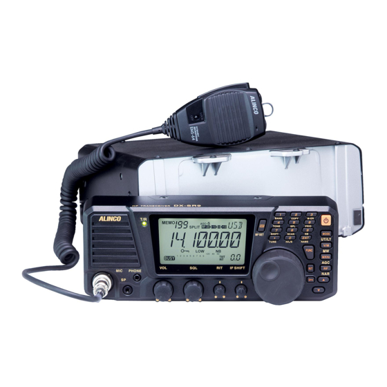
DX-SR9 T / E
Service Manual
CONTENTS
General.................................................................... 2
Transmitter .............................................................. 2
Receiver .................................................................. 2
1) Receiver System .............................................. 3,4
2) Transmitter System .......................................... 5,6
3) Peripheral Circuits ............................................ 7,8
4) PLL Synthesizer Circuits ..................................... 9
5) R5F2L3ACANFP#U1 (XA1400 / XA1442) ... 10-12
SEMICONDUCTOR DATA
1) NJM4558M (XA0097)........................................ 12
2) BD1754HFN (XA1403)...................................... 12
3) NJM78M05DL1A (XA1118)............................... 12
4) NJM7808FA (XA1106) ...................................... 13
5) TC4S66F (XA0115)........................................... 13
6) BU4052BCF (XA0236) ...................................... 13
7) BU4001BF (XA0299) ........................................ 13
8) TA75S01F (XA0332) ......................................... 13
9) LA4425A (XA0410) ........................................... 13
10) TC74HC74AF (XA0459) ................................. 14
11) NJM3357M (XA0742)...................................... 14
12) NJM7805FA (XA0812) .................................... 14
13) UPC2710TB (XA0968) .................................... 14
14) NJM2594V (XA0995) ...................................... 14
15) TC74HC390AF (XA1001) ............................... 14
16) MB15A01PFV1 (XA1010) ............................... 15
17) LM2904PWR (XA1103)................................... 15
18) LM2902PWR (XA1106)................................... 15
19) S80845CLNB (XA1120) ................................. 15
20) TC4SU11F (XA1396) ...................................... 15
21) TC74VHC393FT (XA1397) ............................. 16
22) XC9504B092AR (XA1398).............................. 16
23) AD9833BRMA (XA1399)................................. 16
24) R1EX24256ASAS0A#S0 (XA1401) ................ 16
25) M61545AFP#DF0R (XA1402)......................... 17
26) NJM2068V (XA1404) ...................................... 17
27) TC7WB66FK (XA1407) ................................... 17
28) LM2904PWR (XA1103)................................... 17
29) NJM2783V (XA1525) ...................................... 17
31) LCD Connection (EL0064) .............................. 18
, INC.
1) Front View .................................................... 19,20
2) Main Side ..................................................... 21-23
FRONT Unit........................................................... 24
LCD Unit ................................................................ 24
PA Unit ............................................................. 25,26
MAIN Unit ......................................................... 27-38
Mechanical Unit ..................................................... 38
Packing Unit .......................................................... 38
ADJUSTMENT
1) Required Test Equipment ................................. 39
2) Adjustment Spot ................................................ 40
3) PA Unit Adjustment ........................................... 41
4) MAIN Unit Adjustment .................................. 41,42
5) RX Test Specification ........................................ 43
6) TX Test Specification ................................... 44,45
7) Test Specification ......................................... 45,46
FRONT Unit Side A ............................................... 47
FRONT Unit Side B ............................................... 48
MAIN Side A .......................................................... 49
MAIN Side A No.1 ................................................. 50
MAIN Side A No.2 ................................................. 51
MAIN Side B .......................................................... 52
MAIN Side B No.1 ................................................. 53
MAIN Side B No.2 ................................................. 54
PA Side A .............................................................. 55
FRONT Unit........................................................... 56
MAIN Unit (MAIN CPU) ......................................... 57
MAIN Unit (MAIN 1)............................................... 58
MAIN Unit (MAIN 2)............................................... 59
MAIN Unit (MAIN 3)............................................... 60
MAIN Unit (PLL) .................................................... 61
MAIN Unit (SDR) ................................................... 62
PA Unit (PA) .......................................................... 63
PA Unit (FILTER) .................................................. 64
BLOCK DIAGRAM.........................................65
Advertisement
Table of Contents

Related Manuals for Alinco DX-SR9 T


Summary of Contents for Alinco DX-SR9 T
-
Page 1: Table Of Contents
DX-SR9 T / E Service Manual CONTENTS SPECIFICATIONS EXPLODED VIEW General..............2 1) Front View ............ 19,20 Transmitter .............. 2 2) Main Side ............. 21-23 Receiver ..............2 PARTS LIST CIRCUIT DESCRIPTION FRONT Unit............24 1) Receiver System ..........3,4 LCD Unit .............. -
Page 2: Specifications
SPECIFICATIONS General DX-SR9 T / E DX-SR9T DX-SR9E Operating mode J3E (USB, LSB),A3E (AM), A1A (CW), F3E (FM) Microphone impedance 300Ω 300Ω Number of memory channels 600 channels simplex 160m band (1.8M) 1.80000 - 1.99999MHz 1.80000 - 1.99999MHz Antenna impedance 50Ω... -
Page 3: Circuit Description
CIRCUIT DESCRIPTION b. The First IF Amplifier Circuit XF102 and XF103 are the crystal filters of 71.75MHz. By the combination of two filters, the unit has the characteristics of the band width of 15kHz or more 1) Receiver System 3dB and the value of guaranteed attenuation of 70dB or more. Here the image ratio is determined 70dB or more (approx. - Page 4 f. Demodulator When the AGC is set to SLOW, an analogue switch in the IC108 turns ON and When in SSB or CW mode, the local oscillation signal mentioned below from the R333 and C351 comes in parallel, and R333 with C351 makes discharge DDS circuit is input to the balanced mixer of the IC104.
-
Page 5: Transmitter System
2) Transmitter e. Transmitter First Mixer The first transmit mixer comprising of the Q103, Q108, L104 and L117 is a 1. MAIN Unit balanced type mixer input about 3dBm local oscillator a. Mic Amp The input signal from microphone goes thru mic-gain pot the VR117 and is fed (71.75MHz+TxFreq) to obtain the wanted frequency. - Page 6 2. PA Unit The D179 and R457 help to follow speeding up the keying, while the D176 and R458 determine the discharging time constant in transmission and elongate a. Power Amp the time constant in reception so that it compensates the time constant The signal input is amplified by the Q803 to about 100mW.
-
Page 7: Peripheral Circuits
3) Peripheral Circuits 5. Low Pass Filter The output from the final power amp goes through the low pass filter removing 1. Beep and Sidetone Circuit the harmonics. The input/output for this filter is switched with a relay, and the Sidetone is output by the STON line at pin No.24 of the CPU (MAIM UNIT) in filters not used are shorted to ground thru relays. - Page 8 8. Power Supply and Resetting 15. SDR Mode The IC102, resetting IC for resetting the CPU, turns on and off at 4.5V. When In SDR receiving, 26th pin(SDR) of CPU (IC101) becomes H. Through the OFF (0V) the CPU resets. Then the IC1004’s reset signal goes Low and the analog switch IC1014 , the received signal of 455KHz, which is amplified by CPU stops.
-
Page 9: Pll Synthesizer Circuits
4) PLL Synthesizer circuits 1. Reference frequency oscillator circuit The reference oscillation frequency for the PLL of the second local oscillator reference and DDS clock, etc. is set at 16.777216MHz. The signal is oscillated by the X601, Q609, and Q611 buffered with the Q608. It is used for the DDS clock for BFO oscillation. -
Page 10: R5F2L3Acanfp#U1 (Xa1400 / Xa1442)
5) R5F2L3ACANFP#U1 (XA1400 / XA1442) FRONT CPU (XA1400) FRONT / MAIN CPU Terminal Signal I/O Description 1 P13 UP Key input Terminal Connection 2 P13/RXD0 UART data reception input 3 P13/TXD0 O UART data transmission output (TOP VIEW) 4 P13 5 WKUP 6 VREF 7 MODE... - Page 11 FRONT CPU (XA1400) MAIN CPU (XA1442) Terminal Signal I/O Description Terminal Signal I/O Description P13/AN3 TEMP Temperature detection of transmission AMP 57 SEG33 SEG33 P13/RXD0 UART data reception input 58 SEG32 SEG32 P13/TXD0 O UART data transmission output 59 SEG31 SEG31 P13/DA0 O Output of voltage for squelch...
-
Page 12: Njm4558M (Xa0097)
SEMICONDUCTOR DATA MAIN CPU (XA1442) Terminal Signal I/O Description RXD1 Clone data reception input 1) NJM4558M (XA0097) TXD1 O Clone data transmission output Operation Amplifiers BPF0 O 1.6MHz BAND BPF1 O 1.9MHz BAND BPF2 O 3.5MHz BAND BPF3 O 7MHz BAND BPF4 O 10MHz BAND BPF5... -
Page 13: Njm7808Fa (Xa1106)
4) NJM7808FA (XA1106) 7) BU4001BF (XA0299) 8V Voltage Regulator Quad 2-input NOR GATE 14 VDD Pin Assignment 13 A4 12 B4 11 O4 1. OUTPUT 10 O3 2. COMMON 9 B3 3. INPUT 8 A3 8) TA75S01F (XA0332) Single Operational Amplifiers 5) TC4S66F (XA0115) V CC Bilateral Switch... -
Page 14: Tc74Hc74Af (Xa0459)
10) TC74HC74AF (XA0459) 13) UPC2710TB (XA0968) Wide Band Amp Dual D-type Flip Flop 1CLR 1 14 V Pin Name 1D 2 13 2CLR CK D INPUT 1CK 3 12 2D 1PR 4 11 2CK OUTPUT 1Q 5 10 2PR CK D 1Q 6 GND 7 14) NJM2594V (XA0995) -
Page 15: Mb15A01Pfv1 (Xa1010)
16) MB15A01PFV1 (XA1010) 18) LM2902PWR (XA1106) PLL Synthesizer Quad Operational Amplifiers 1. OSC IN 9. Clock 2. OSC OUT 10. Data 3. Vp 11. LE 4. Vcc 12. FC 5. Do 13. N. C. 15A01 6. GND 14. fout **** 7. -
Page 16: Tc74Vhc393Ft (Xa1397)
21) TC74VHC393FT (XA1397) 23) AD9833BRMZ (XA1399) Dual Binary Counter Programmable Waveform Generator 1 1CK 8 2QD 2 1CLR 9 2QC 3 1QA 10 2QB COMP 1 VOUT 4 1QB 11 2QA VDD 2 AGND 5 1QC 12 2CLR AD9833 CAP/2.5V 3 FSYNC 6 1QD 13 2CK... -
Page 17: M61545Afp#Df0R (Xa1402)
25) M61545AFP#DF0R (XA1402) 28) LM2904PWR (XA1103) Electronic Volume Dual Operational Amplifiers CLOCK ≈6- A ≈6- A ≈100- A μ μ μ Current Current Current Regulator Regulator Regulator 1OUT VR 2 – 1IN− 2OUT GND 3 1IN+ 2IN− DATA 4 CLOCK VOL AMP 2 LOGIC 2IN+... -
Page 18: Transistor, Diode And Led Outline Drawing
30) Transistor, Diode and LED outline Drawings 31) LCD Connection (EL0064) Top View VRPG3312X 1SS133 DA204U DAN202U DAP202U 1SS355 DAP236 XL0051 XD0038 XD0130 XD0230 XD0231 XD0254 XD0266 1SS356 1SV262 HSB88WSTR DAN235E RLS-73 UDZS 6.2B CRG01 XD0272 XD0300 XD0302 XD0320 XD0363 XD0388 XD0391 VDZT2R5.1B... -
Page 19: Exploded View
EXPLODED VIEW 1) Front View a.LCD XL0051 TL0041 DG0050 TL0037 EL0064 RV0051 RV0053 FG0499 UR0029 ST0103 UJ0072 b.Front View UJ0073 DX-SR9 HF TRANSCEIVER UE0035Y YX0053 DP0222 (UR0029) SP0022 (UE0035Y) NK0084 NK0086 NK0085... -
Page 21: Main Side
2) MAIN SIDE a.Top View AA0085 x8 DF0009 DF0008 DF0007 x2 FM0162 KS0107 AA0043 x16 AA0084 x2 AZ0054 x2 QB0036 UE0602 TZ0066 UX1423 UJ0032 UJ0045 UJ0030 ET0014A SS0113A UX1421 UE0041 UX1422... - Page 22 b.Bottom View AA0085 x9 UX1421 AA0043 x17 UX1422 UE0603 FM0220 x4 TZ0066 UJ0032 UJ0030 UX1424 SP0008 UE0258 DD0019 AA0005 x2 AD0005 DD0023 UX1423 FP0151 UJ0030...
- Page 23 c.Front View AA0085 x2 UX1412 FG0506 x2...
-
Page 24: Parts List
PARTS LIST FRONT Unit Ref. Ref. Parts No. Description Parts Name Version Parts No. Description Parts Name Version CU3535 Chip C GRM36B102K50PT RK3557 Chip R 1005 1/16W 39K OHM J CS0424 Chip Tantalum TMCMA1C106MTR RK3550 Chip R 1005 1/16W 10K OHM J CU3535 Chip C GRM36B102K50PT... -
Page 25: Pa Unit
PA Unit Ref. Ref. Parts No. Description Parts Name Version Parts No. Description Parts Name Version C801 CU0142 Chip C 2012 B 50V 0.1UF K C926 CU3047 Chip C 1608 B 50V 0.010UF C802 CU0095 Chip C 2012 B 50V 0.022UF C927 CU4027 Chip C... - Page 26 PA Unit Ref. Ref. Parts No. Description Parts Name Version Parts No. Description Parts Name Version FH802 UH0014 Fuse Holder PFC5000-0301 R832 RK0031 Chip R 2125 1/8W 680 OHM J L801 QR0024 Transformer RF TRANS QR0024 R833 RK3038 Chip R 1608 1/10W 1.0KOHM J L802 QR0014C Transformer...
-
Page 27: Main Unit
MAIN Unit Ref. Ref. Parts No. Description Parts Name Version Parts No. Description Parts Name Version C101 CU3547 Chip C GRM155B11C103KA01D C178 CU3101 Chip C 1608 B 50V 0.047UF K C102 CU3547 Chip C GRM155B11C103KA01D C179 CU3038 Chip C 1608 B 50V 0.0018UF C103 CU3111 Chip C... - Page 28 MAIN Unit Ref. Ref. Parts No. Description Parts Name Version Parts No. Description Parts Name Version C255 CU3554 Chip C GRM155B11A104KA01D C332 CU3553 Chip C GRM36B473K10PT C256 CU3029 Chip C 1608 B 50V 330PF K C333 CU3553 Chip C GRM36B473K10PT C257 CU3028 Chip C...
- Page 29 MAIN Unit Ref. Ref. Parts No. Description Parts Name Version Parts No. Description Parts Name Version C409 CU3137 Chip C GRM188B31C105KA92D C486 CS0424 Chip Tantalum TMCMA1C106MTR C410 CU3547 Chip C GRM155B11C103KA01D C487 CU0118 Chip C GRM21BB31C475KA87L C411 CU3547 Chip C GRM155B11C103KA01D C488 CU3138...
- Page 30 MAIN Unit Ref. Ref. Parts No. Description Parts Name Version Parts No. Description Parts Name Version C662 CU3541 Chip C GRM36B332K50PT C1047 CU3554 Chip C GRM155B11A104KA01D C663 CU3521 Chip C GRM1552C1H680JZ01D C1048 C664 CU3521 Chip C GRM1552C1H680JZ01D C1049 CU3554 Chip C GRM155B11A104KA01D C665 CU3520...
- Page 31 MAIN Unit Ref. Ref. Parts No. Description Parts Name Version Parts No. Description Parts Name Version D110 XD0320 Diode DAN235E-TL D187 XD0482 Diode 1SS405(TPH3,F) D111 XD0302 Diode HSB88WSTR D188 XD0231 Diode DAP202U D112 XD0266 Diode DAP236UT106 D189 XD0482 Diode 1SS405(TPH3,F) D113 XD0272 Diode...
- Page 32 MAIN Unit Ref. Ref. Parts No. Description Parts Name Version Parts No. Description Parts Name Version JK103 UJ0030 Jack JPJ2545-01-510 L174 QC0086 Chip Inductor 3225 100 UH JK1003 UJ0066 Jack HSJ1453-01-010 L175 QC0128 Chip Inductor 3225 .33 UH JK1004 UJ0066 Jack HSJ1453-01-010 L176...
- Page 33 MAIN Unit Ref. Ref. Parts No. Description Parts Name Version Parts No. Description Parts Name Version Q146 XT0210 Transistor 2SC6026MFV-GR Q1013 Q147 XT0127 Transistor 2SC3419-Y Q1014 Q148 XU0210 Transistor RN1107FV Q1015 Q149 XT0136 Transistor 2SD1664 T101 Q Q1016 XE0053 3SK293TE85L Q150 XT0210 Transistor...
- Page 34 MAIN Unit Ref. Ref. Parts No. Description Parts Name Version Parts No. Description Parts Name Version R160 RK3534 Chip R 1005 1/16W 470 OHM J R237 RK3522 Chip R 1005 1/16W 47 OHM J R161 RK3561 Chip R 1005 1/16W 82K OHM J R238 RK3028 Chip R...
- Page 35 MAIN Unit Ref. Ref. Parts No. Description Parts Name Version Parts No. Description Parts Name Version R314 RK3571 Chip R 1005 1/16W 560K OHMJ R392 RK3542 Chip R 1005 1/16W 2.2K OHMJ R315 RK3562 Chip R 1005 1/16W 100K OHMJ R393 R316 RK3542...
- Page 36 MAIN Unit Ref. Ref. Parts No. Description Parts Name Version Parts No. Description Parts Name Version R469 RK3558 Chip R 1005 1/16W 47K OHM J R603 RK3534 Chip R 1005 1/16W 470 OHM J R470 RK3554 Chip R 1005 1/16W 22K OHM J R604 RK3522 Chip R...
- Page 37 MAIN Unit Ref. Ref. Parts No. Description Parts Name Version Parts No. Description Parts Name Version R687 RK3539 Chip R 1005 1/16W 1.2K OHMJ R1047 RK3550 Chip R 1005 1/16W 10K OHM J R688 RK3534 Chip R 1005 1/16W 470 OHM J R1048 RK3501 Chip R...
-
Page 38: Mechanical Unit
MAIN Unit Ref. Ref. Parts No. Description Parts Name Version Parts No. Description Parts Name Version R1125 DP0222 LCD PANEL SR9 R1126 RK3558 Chip R 1005 1/16W 47K OHM J ES0035A 57-8BC-35 2.0T R1127 RK3550 Chip R 1005 1/16W 10K OHM J ET0014A FAN AD812MB-C70(TP) R1128... -
Page 39: Required Test Equipment
Adjustments 14. Personal Computer PC requirements : OS : Windows Vista, 7 or 8 1) Required Test Equipment CPU : Intel Core i5 2.4 GHz equivalent or faster Memory : 2GByte or more The following items are required to adjust radio parameters Display : 1024×768 pixel, color 32bit or better Sound card :... -
Page 40: Adjustment Spot
2) Adjustment Spot PA Unit Adjustment Spot MAIN Unit Adjustment Spot JP109 CN101 VR117 VR108 VR109 VR111 VR105 L180 L179 VR116 VR104 VR106 VR103 VR115 VR107 VR118 VR102 VR110 VR113 VR112 L127 VR120 VR114 CN107 VR119 L126 L120 TP601 TP603 L112 L156 L143... -
Page 41: Pa Unit Adjustment
3) PA Unit Adjustment 4) MAIN Unit Adjustment Idling Current Adjustment Setting (a) RX Adjustment Adjustment the idle current without Oscilloscope DC current meter DC power supply DXSR9 input signal. SP OUT DXSR9 DC current meter DXSR9 PA unit adjustment tool Distortion meter Audio volmeter DC current meter... - Page 42 4) MAIN Unit Adjustment ITEM CONDITION UNIT ADJ.SPOT ADJUSTING METHOD 14.1000MHz MAIN VR114 Connect JP109 by soldering before (b) TX Adjustment Power 50W MODE : FM adjustment. Mod : OFF Adjust to 50.0±1.0 W. AF signal DXSR8 Power meter Oscilloscope Remove the solder of JP109 after generator adjustment.
-
Page 43: Rx Test Specification
5) RX Test Specification TEST ITEM CONDITION TEST STANDARD NOTE 14.1000MHz Confirm Switch AGC-S. When SG is turned MODE : USB OFF, the meter moves slowly. TEST ITEM CONDITION TEST STANDARD NOTE RF : +10dBu Switch AGC-F. When SG is turned Less than +6dBu RX Sensitivity 1.0000MHz LSB... -
Page 44: Tx Test Specification
6) TX Test Specification TEST ITEM CONDITION TEST STANDARD NOTE TONE(88.5Hz) 28.1000MHz 0.3 〜 0.7KHz/DEV 3KHz LPF ON MODE : FM TEST ITEM CONDITION TEST STANDARD NOTE MOD : OFF Frequency 14.1000MHz Within±50Hz Deviation MODE : AM TONE ON TX Output 1.9MHz BAND 90 〜... -
Page 45: Test Specification
6) TX Test Specification 7) Test Specification TEST ITEM CONDITION TEST STANDARD NOTE TEST ITEM CONDITION TEST STANDARD NOTE SDR RX UNIT: Check if can hear Transmission DATA VOX 14.1000MHz Confirm Transmission MODE : SDR the sound of the 1 Set mode 26 MODE : USB (FM MODE →... - Page 46 7) Test Specification TEST ITEM CONDITION TEST STANDARD NOTE SDR TX UNIT: TX Power: More MODE : SDR than 90W. (FM MODE → FUNC → MODE key) TRX SDR: Freauency:14.1000M Mode:FM TX PWR:High TRX SDR CONTROLLER:TX TRX SDR Setting...
-
Page 47: Pc Board View
PC BOARD VIEW FRONT SIDE A... -
Page 48: Front Unit Side B
FRONT SIDE B... -
Page 49: Main Side A
MAIN SIDE A MAIN UNIT SIDE A No.2 MAIN UNIT SIDE A No.1... -
Page 50: Main Side A No.1
MAIN SIDE A No.1... -
Page 51: Main Side A No.2
MAIN SIDE A No.2... -
Page 52: Main Side B
MAIN SIDE B MAIN UNIT SIDE B No.2 MAIN UNIT SIDE B No.1... -
Page 53: Main Side B No.1
MAIN SIDE B No.1... -
Page 54: Main Side B No.2
MAIN SIDE B No.2... -
Page 55: Pa Side A
PA SIDE A L801... -
Page 56: Schematic Diagram Front Unit
SCHEMATIC DIAGRAM FRONT Unit LCD1 EL0064 EMD9 EMD9 2.7V PW SW TXLED 0.022 IC2A NJM4558M IC2B NJM4558M 2SC6026MFV SEG14 SEG40 SEG14 (SEG14) SEG40 (SEG40) SEG13 SEG41 SEG13 (SEG13) SEG41 (SEG41) MUTE SEG12 SEG42 SEG12 (SEG12) SEG42 (SEG42) SEG11 SEG43 0.001 SEG11 (SEG11) SEG43 (SEG43) SEG10 SEG44 SEG10 (SEG10) SEG44 (SEG44) SEG9 SEG45 SEG9 (SEG9) SEG45 (SEG45) -
Page 57: Main Unit (Main Cpu)
SCHEMATIC DIAGRAM JK1005 MAIN Unit (MAIN CPU) HSJ1332-01-040 (JP101) (JP102) (JP103) (JP104) (JP105) (JP106) (JP107) (JP108) DXSR8 Solder Solder Solder JK101 R103 DXSR8 T Solder DXSR8 E Solder R104 CW K R105 D103 R106 1SS405 HSJ1332-01-040 FB101 BL02RN 2R1M2B CN 101 MAIN2[8B], MAIN3[1A] HJC0282-010024 MAIN1[8A], ... -
Page 58: Main Unit (Main 1)
T P 101 3.0V (TX : FM MODE) R 133 R 134 C 113 R 135 Q103 C 114 L101 L102 R 136 L103 XF 101 D108 3S K 293 L104 L105 L106 0.0047 MAIN3[3A], MAIN̲C P U[1B ] C N103 QR 0017 71.75MHz DAN235E QA0108 QA0107 K E YM... -
Page 59: Main Unit (Main 2)
SCHEMATIC DIAGRAM M A IN 4 [5B ], P L L [6C ] R S W IC 122 Q 196 R 7 23 R N 1107M F V 100 k B F O M A IN 4 [5B ], P L L [6C ] M A IN 4 [5B ], P L L [6C ] T S W R 2 51... -
Page 60: Main Unit (Main 3)
D189 1S S 405 T P 106 T P 103 IC 115 T P 107 T P 104 IC 116 T P 105 R 397 D155 NJ M7808F A NJ M7805F A J K 102 1S S 405 T XS MAIN̲C P U[4B ] MAIN1[8A], MAIN̲C P U[1B ] MAIN̲C P U[5B ]... -
Page 61: Main Unit (Pll)
SCHEMATIC DIAGRAM -4V (RX : 14.1MHz (USB MODE)) Q 601 2S C 6026MF V MAIN Unit (PLL) IC 601B N J M2068V R 603 R 601 C 601 C 602 T P 602 1.5K 1.5/20V 1.5/20V P D 1 R 607 C 611 MAIN 1[4B ] R 609 R 610 C 615... -
Page 62: Main Unit (Sdr)
SCHEMATIC DIAGRAM MAIN Unit (SDR) MAIN2[6D] AF OUT VR 1001 C1044 R 1048 Q1004 R N1107MFV C1004 180p IC1009 R 1043 R 1003 R 1004 Q1003 C1005 R N2107 TC4S66F D194 JK1003 IC1001A LM2904PWR 1SS405 R 1046 IQ OUT C1006 HSJ1453-01-010 R 1008 C1007 180p R 1010... -
Page 63: Pa Unit (Pa)
SCHEMATIC DIAGRAM PA Unit (PA) TP801 VR805 CN803 TMP-J01X-V6 Q801 R804 C802 R805 RD16HHF1 18(3W) upside : C860 L802 C803 0.022 Q802 L801 0.022 1K(1/2W) downside : C861 QR0014C L803 RD100HHF1 QR0024 C804 R806 TP802 QR0025 C805 0.022 Q803 UE0047 4.2V R837 L804... -
Page 64: Pa Unit (Filter)
L923 PA[7B] CN901 L901 L902 L903 R901 QR0013A QR0021 QR0004 RL901 R902 C901 C902 RL902 470P 150P 180(1/2W) R904 R905 RL903 L904 L905 R906 68(1/2W) 0.22u 0.22u AG201344 D902 AG201344 RB717F 1.8M AG201344 CN904 L907 L908 TMP-J01X-V6 (1.9MHz BAND) QR0006 QR0007 R907 RL904... -
Page 65: Block Diagram
BLOCK DIAGRAM Q1016 IQ IN IQ OUT SDR TSW IQ AMP SDR TSW NB GATE CONTROL SDR RSW BUFF AMP IQ DET SDR RSW IC1008 IC1017 IC1004 IC1016 IC1014 Q1002 IC1003 IC1001 IC1010 1.5M ATT SW Q121 PRE AMP FM DET Q128 2.5M 1.6M... - Page 66 ALINCO,INC. Head Office:Yodoyabashi-Dai building 13th Floor 4-9, 4-Chome, Koraibashi, Chuo-ku, Osaka 541-0043, JAPAN Phone:+81-6-7636-2362 Fax:+81-6-6208-3802 http://www.alinco.com E-mail:export@alinco.co.jp Dealer/Distributor Copyright Alinco, Inc. Osaka Japan PM0110 Printed in Japan FNEH-NI...
Need help?
Do you have a question about the DX-SR9 T and is the answer not in the manual?
Questions and answers