
Related Manuals for Xilinx VC709


Summary of Contents for Xilinx VC709
- Page 1 VC709 Evaluation Board for the Virtex-7 FPGA User Guide UG887 (v1.6) March 11, 2019...
-
Page 2: Please Read: Important Legal Notices
(including loss of data, profits, goodwill, or any type of loss or damage suffered as a result of any action brought by a third party) even if such damage or loss was reasonably foreseeable or Xilinx had been advised of the possibility of the same. - Page 3 Caution. Updated the description of Dual DDR3 Memory SODIMMs. In Appendix C, Xilinx Design Constraints changed the title of the appendix, updated the description, and removed the VC709 Board XDC Listing. Updated Appendix F, Regulatory and Compliance Information. Updated Appendix G, Additional Resources.
- Page 4 VC709 Evaluation Board www.xilinx.com UG887 (v1.6) March 11, 2019...
-
Page 5: Table Of Contents
VC709 Board Features ........ - Page 6 ..............83 www.xilinx.com VC709 Evaluation Board Send Feedback...
-
Page 7: Chapter 1: Vc709 Evaluation Board Features
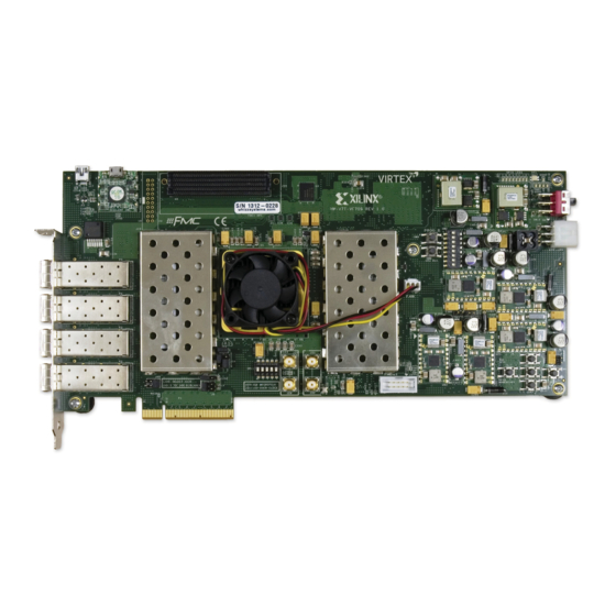
VC709 Evaluation Board Features Overview The VC709 evaluation board for the Virtex®-7 FPGA provides a hardware environment for developing and evaluating designs targeting the Virtex-7 XC7VX690T-2FFG1761C FPGA. The VC709 board provides features common to many embedded processing systems, including dual DDR3 small outline dual-inline memory module (SODIMM) memories, an 8-lane PCI Express®... - Page 8 VC709 Evaluation Board Features Chapter 1: • Gen3 8-lane (x8) • 4 X SFP+ connectors • USB-to-UART bridge • C bus • C MUX • C EEPROM (1 KB) • USER I C programmable LVDS oscillator • 2 X DDR3 SODIMM socket •...
-
Page 9: Electrostatic Discharge Caution
Put the adapter down only on an antistatic surface such as the bag supplied in your kit. • If you are returning the adapter to Xilinx Product Support, place it back in its antistatic bag immediately. X-Ref Target - Figure 1-1... -
Page 10: Feature Descriptions
VC709 Evaluation Board Features Chapter 1: Feature Descriptions Figure 1-2 shows the VC709 board. Each numbered feature that is referenced in Figure 1-2 described in Table 1-1 and following sections. The image in Figure 1-2 is for reference only and might not reflect the current revision of the Note: board. - Page 11 Feature Descriptions Table 1-1: VC709 Board Component Descriptions (Cont’d) Schematic Reference 0381499 Callout Component Description Notes Designator Page Number J25, J26 GTH transceiver SMA reference clock Rosenberger 32K10K-400L5 Jitter-attenuated clock (back side of board) Silicon Labs SI5324C-C-GM GTH transceiver Quad 111–Quad 119 Embedded within FPGA U1 30, 36–38...
-
Page 12: Virtex-7 Xc7Vx690T-2Ffg1761C Fpga
Master BPI using the onboard linear BPI flash memory • JTAG using a type-A to micro-B USB cable for connecting the host PC to the VC709 board configuration port Each configuration interface corresponds to one or more configuration modes and bus widths as... - Page 13 There are 17 I/O banks available on the Virtex-7 device. Fourteen I/O banks are available on the VC709 board, and banks 12, 16, and 18 are not used. The voltages applied to the FPGA I/O banks used by the VC709 board are listed in Table 1-3.
-
Page 14: Dual Ddr3 Memory Sodimms
Datapath width: 64 bits • Data rate: Up to 1600 MT/s The VC709 XC7VX690T FPGA memory interface performance is documented in the Virtex-7 T and XT FPGAs Data Sheet: DC and AC Switching Characteristics (DS183) [Ref Each DDR3 interface is implemented across three I/O banks: 37, 38, and 39 for J1 and 31, 32 and 33 for J3. - Page 15 SSTL15 DQ20 DDR3_A_D21 SSTL15 DQ21 DDR3_A_D22 SSTL15 DQ22 DDR3_A_D23 SSTL15 DQ23 DDR3_A_D24 SSTL15 DQ24 DDR3_A_D25 SSTL15 DQ25 DDR3_A_D26 SSTL15 DQ26 DDR3_A_D27 SSTL15 DQ27 DDR3_A_D28 SSTL15 DQ28 DDR3_A_D29 SSTL15 DQ29 VC709 Evaluation Board www.xilinx.com Send Feedback UG887 (v1.6) March 11, 2019...
- Page 16 VC709 Evaluation Board Features Chapter 1: Table 1-4: DDR3 SODIMM Socket J1 Connections to the FPGA (Cont’d) DDR3 SODIMM Memory J1 XCVX690T (U1) Pin Net Name I/O Standard Pin Number Pin Number DDR3_A_D30 SSTL15 DQ30 DDR3_A_D31 SSTL15 DQ31 DDR3_A_D32 SSTL15...
- Page 17 DIFF_SSTL15 DQS6_N DDR3_A_DQS6_P DIFF_SSTL15 DQS6_P DDR3_A_DQS7_N DIFF_SSTL15 DQS7_N DDR3_A_DQS7_P DIFF_SSTL15 DQS7_P DDR3_A_CLK0_N DIFF_SSTL15 CK0_N DDR3_A_CLK0_P DIFF_SSTL15 CK0_P DDR3_A_CLK1_N DIFF_SSTL15 CK1_N DDR3_A_CLK1_P DIFF_SSTL15 CK1_P DDR3_A_CKE0 SSTL15 CKE0 DDR3_A_CKE1 SSTL15 CKE1 VC709 Evaluation Board www.xilinx.com Send Feedback UG887 (v1.6) March 11, 2019...
- Page 18 VC709 Evaluation Board Features Chapter 1: Table 1-4: DDR3 SODIMM Socket J1 Connections to the FPGA (Cont’d) DDR3 SODIMM Memory J1 XCVX690T (U1) Pin Net Name I/O Standard Pin Number Pin Number DDR3_A_RAS_B SSTL15 RAS_B DDR3_A_WE_B SSTL15 WE_B DDR3_A_CAS_B SSTL15...
- Page 19 DQ24 BA24 DDR3_B_D25 SSTL15 DQ25 AY23 DDR3_B_D26 SSTL15 DQ26 AY24 DDR3_B_D27 SSTL15 DQ27 AY25 DDR3_B_D28 SSTL15 DQ28 BA25 DDR3_B_D29 SSTL15 DQ29 BB21 DDR3_B_D30 SSTL15 DQ30 BA21 DDR3_B_D31 SSTL15 DQ31 VC709 Evaluation Board www.xilinx.com Send Feedback UG887 (v1.6) March 11, 2019...
- Page 20 VC709 Evaluation Board Features Chapter 1: Table 1-5: DDR3 SODIMM Socket J3 Connections to the FPGA (Cont’d) DDR3 SODIMM Memory J3 XCVX690T (U1) Pin Net Name I/O Standard Pin Number Pin Name AY14 DDR3_B_D32 SSTL15 DQ32 AW15 DDR3_B_D33 SSTL15 DQ33...
- Page 21 CK0_P AT17 DDR3_B_CLK0_P DIFF_SSTL15 CK0_N AV18 DDR3_B_CLK1_N DIFF_SSTL15 CK1_P AU18 DDR3_B_CLK1_P DIFF_SSTL15 CK1_N AW17 DDR3_B_CKE0 SSTL15 CKE0 AW18 DDR3_B_CKE1 SSTL15 CKE1 AV19 DDR3_B_RAS_B SSTL15 RAS_B AU19 DDR3_B_WE_B SSTL15 WE_B VC709 Evaluation Board www.xilinx.com Send Feedback UG887 (v1.6) March 11, 2019...
-
Page 22: Linear Bpi Flash Memory
AU16 DDR3_B_TEMP_EVENT_B SSTL15 EVENT_B The VC709 DDR3 SODIMM interfaces adhere to the constraints guidelines documented in the DDR3 Design Guidelines section of 7 Series FPGAs Memory Interface Solutions User Guide (UG586) [Ref 4]. The VC709 DDR3 SODIMM interfaces are 40Ω impedance implementations. - Page 23 FLASH_A17 LVCMOS18 BA42 FLASH_A18 LVCMOS18 AU42 FLASH_A19 LVCMOS18 AT41 FLASH_A20 LVCMOS18 BA40 FLASH_A21 LVCMOS18 BA39 FLASH_A22 LVCMOS18 BB39 FLASH_A23 LVCMOS18 AW42 FLASH_A24 LVCMOS18 AW41 FLASH_A25 LVCMOS18 AM36 FLASH_D0 LVCMOS18 VC709 Evaluation Board www.xilinx.com Send Feedback UG887 (v1.6) March 11, 2019...
- Page 24 VC709 Evaluation Board Features Chapter 1: Table 1-6: BPI Flash Memory Connections to the FPGA (Cont’d) BPI Flash Memory (U3) FPGA (U1) Pin Net Name I/O Standard Pin Number Pin Name AN36 FLASH_D1 LVCMOS18 AJ36 FLASH_D2 LVCMOS18 AJ37 FLASH_D3 LVCMOS18...
- Page 25 Feature Descriptions Figure 1-4 shows the linear BPI flash memory on the VC709 board. For more details, see the Micron Technology, Inc MT28GU01GAAA1EGC data sheet[Ref 13]. X-Ref Target - Figure 1-4 MT28GU01GAAA1EGC 64-Pin BGA (8 x 10 mm) FLASH_D0_R FLASH_A0...
-
Page 26: Usb Jtag
1-2, callout 4] JTAG configuration is provided solely through a Digilent onboard USB-to-JTAG configuration logic module (U26) where a host computer accesses the VC709 board JTAG chain through a type-A (host side) to micro-B (VC709 board side) USB cable. The JTAG chain of the VC709 board is illustrated in Figure 1-5. -
Page 27: Clock Generation
JTAG_TDO SN74AVC1T45 Voltage Translator UG855_c1_06_101714 Figure 1-6: JTAG Circuit Clock Generation The VC709 board provides six clock sources for the FPGA. Table 1-7 lists the source devices for each clock. VC709 Evaluation Board www.xilinx.com Send Feedback UG887 (v1.6) March 11, 2019... - Page 28 VC709 Evaluation Board Features Chapter 1: Table 1-7: VC709 Board Clock Sources Clock Clock Name Description Source SiT9102 2.5V LVDS 200 MHz fixed frequency oscillator (Si Time) System clock System Clock (SYSCLK_P and SYSCLK_N). Si570 3.3V LVDS I C Programmable Oscillator, ( C address 0x5D), 156.250 MHz default...
- Page 29 [Figure 1-2, callout 5] The VC709 board has an LVDS 200 MHz oscillator (U51) soldered onto the back side of the board and wired to an FPGA MRCC clock input on bank 38. This 200 MHz signal pair is named SYSCLK_P and SYSCLK_N, which are connected to FPGA U1 pins H19 and G18 respectively.
- Page 30 [Figure 1-2, callout 6] The VC709 board has a programmable low-jitter 3.3V differential oscillator (U34) connected to the FPGA MRCC inputs of bank 14. This USER_CLOCK_P and USER_CLOCK_N clock signal pair are connected to FPGA U1 pins AK34 and AL34 respectively. On power-up, the user clock defaults to an output frequency of 156.250 MHz.
- Page 31 FPGA U1 pins (no series capacitors and no external parallel termination resistor).The user-provided 1.8V differential clock circuit is shown in Figure 1-9. X-Ref Target - Figure 1-9 USER_SMA_CLOCK_P Connector USER_SMA_CLOCK_N Connector UG887_c1_09_090612 Figure 1-9: User SMA Clock Source VC709 Evaluation Board www.xilinx.com Send Feedback UG887 (v1.6) March 11, 2019...
- Page 32 [Figure 1-2, callout 8] The VC709 board includes a pair of SMA connectors for a GTH clock wired to GTH Quad bank 113. This differential clock has signal names SMA_MGT_REFCLK_P and SMA_REFCLK_N, which are connected to FPGA U1 pins AK8 and AK7 respectively.
-
Page 33: Memory Clock (Sysclk_233_P And Sysclk_233_N)
[Figure 1-2, callout 27] The VC709 board has a LVDS 233.3333 MHz oscillator (U13) soldered onto the back side of the board and wired to an FPGA MRCC clock input on bank 32. This 233.3333 MHz signal pair is named SYSCLK_233_P and SYSCLK_233_N. The P and N signals are connected to FPGA U1 pins AY18 and AY17 respectively. -
Page 34: Fpga Emcc Clock
SODIMM socket J3. The VC709 board has a LVCMOS 80 MHz oscillator (U40) soldered onto the board and wired to the FPGA EMCCLK clock input pin AP37 on bank 14. This 80 MHz single-ended signal is named FPGA_EMCCLK. -
Page 35: Gth Transceivers
The GTH transceivers in 7 series FPGAs are grouped into four channels described as Quads. The reference clock for a Quad can be sourced from the Quad above or Quad below the GTH Quad of interest. There are six GTH Quads on the VC709 board with connectivity as shown here: •... - Page 36 VC709 Evaluation Board Features Chapter 1: • Contains 4 GTH transceivers for PCIe lanes 0–3 • Quad 117: • MGTREFCLK0 - No clock • MGTREFCLK1 - No clock • Contains 2 GTH transceivers for FMC1 HPC (DP8–DP9) • Quad 118: •...
- Page 37 GTHE2_CHANNEL_X1Y37 FMC1 HPC DP1 GTHE2_CHANNEL_X1Y36 FMC1 HPC DP0 MGTREFCLK0 MGTREFCLK1 For more information on the GTH transceivers see 7 Series FPGAs GTX/GTH Transceivers User Guide ( UG476 ) [Ref VC709 Evaluation Board www.xilinx.com Send Feedback UG887 (v1.6) March 11, 2019...
-
Page 38: Pci Express Endpoint Connectivity
100Ω differential pair. The 7 series FPGAs GTH transceivers are used for multi-gigabit per second serial interfaces. The XC7VX690T-2FFG1761C FPGA (-2 speed grade) included with the VC709 board supports up to Gen3 x8. The PCIe clock is input from the edge connector. It is AC coupled to the FPGA through the MGTREFCLK1 pins of Quad 115. - Page 39 GTHE2_CHANNEL_X1Y16 PCIE_RX7_P PETp7 receive pair Integrated Endpoint block GTHE2_CHANNEL_X1Y16 PCIE_RX7_N PETn7 receive pair Integrated Endpoint block GTHE2_CHANNEL_X1Y23 PCIE_TX0_P PERp0 transmit pair Integrated Endpoint block GTHE2_CHANNEL_X1Y23 PCIE_TX0_N PERn0 transmit pair VC709 Evaluation Board www.xilinx.com Send Feedback UG887 (v1.6) March 11, 2019...
- Page 40 VC709 Evaluation Board Features Chapter 1: Table 1-10: PCIe Edge Connector Connections (Cont’d) PCIe Edge Connector (P1) Net Name FPGA (U1) Pin Function FFG1761 Placement Name Integrated Endpoint block GTHE2_CHANNEL_X1Y22 PCIE_TX1_P PERp1 transmit pair Integrated Endpoint block GTHE2_CHANNEL_X1Y22 PCIE_TX1_N PERn1...
- Page 41 GTHE2_CHANNEL_X1Y22 MGTXTXP3_115_W2 PCIE_TX0_P PERp0 GTHE2_CHANNEL_X1Y23 MGTXTXN3_115_W1 PCIE_TX0_N PERn0 GTHE2_CHANNEL_X1Y23 MGTXRXP3_115_Y4 PCIE_RX0_P PETp0 GTHE2_CHANNEL_X1Y23 MGTXRXN3_115_Y3 PCIE_RX0_N PETn0 GTHE2_CHANNEL_X1Y23 MGTREFCLK0P_115_Y8 MGT_BANK_115 MGTREFCLK0N_115_Y7 MGT_BANK_115 MGTREFCLK1P_115_AB8 PCIE_CLK_Q0_N REFCLK- MGT_BANK_115 MGTREFCLK1N_115_AB7 PCIE_CLK_Q0_P REFCLK+ MGT_BANK_115 VC709 Evaluation Board www.xilinx.com Send Feedback UG887 (v1.6) March 11, 2019...
- Page 42 VC709 Evaluation Board Features Chapter 1: Table 1-12 lists the PCIe edge connector connections for Quad 114. Table 1-12: GTH Quad 114 PCIe Edge Connector Connections PCIe Edge Connector FPGA (P1) Quad 114 Pin Name Net Name FFG1761 Placement (U1) Pin...
-
Page 43: Sfp/Sfp+ Module Connectors
Feature Descriptions SFP/SFP+ Module Connectors [Figure 1-2, callout 12] The VC709 board supports four small form-factor pluggable (SFP+) connector and cage assemblies P2–P5 that accept SFP or SFP+ modules. Figure 1-16 shows an example of the SFP+ module connector circuitry replicated for each module. - Page 44 VC709 Evaluation Board Features Chapter 1: Table 1-13 lists the SFP+ module RX and TX connections to the FPGA. Table 1-13: FPGA U1 to SFP+ Module Connections SFP+ Module XCVX690T (U1) Pin Net Name Pin Number Pin Name SFP+ Module 1 (P3)
- Page 45 MOD_ABS AE39 SFP4_RS0 LVCMOS18 AE40 SFP4_RS1 LVCMOS18 AD40 SFP4_LOS LVCMOS18 AC40 SFP4_TX_DISABLE LVCMOS18 TX_DISABLE The six control/status signals to/from each SFP+ connector are routed through a level shifter. Note: VC709 Evaluation Board www.xilinx.com Send Feedback UG887 (v1.6) March 11, 2019...
-
Page 46: Usb-To-Uart Bridge
The VC709 board contains a Silicon Labs CP2103GM USB-to-UART bridge device (U44) which allows a connection to a host computer with a USB port. The USB cable is supplied in the VC709 evaluation kit (type-A end to host computer, type mini-B end to VC709 board connector J17). The CP2103GM is powered by the USB 5V provided by the host PC when the USB cable is plugged into the USB port on the VC709 board. -
Page 47: I2C Bus
The four SFP+ connectors SFP1 (P3), SFP2 (P2), SFP3 (P4), and SFP4 (P5) are addressed through a secondary PCA9546A 1-to-4 channel I C bus switch (U14). The VC709 board I C bus topology is shown in Figure 1-17. -
Page 48: Status Leds
VC709 Evaluation Board Features Chapter 1: Table 1-17: I C Bus Addresses (Cont’d) C Switch C Bus C Address Position EEPROM_IIC_SDA/SCL 0b1010100 PCA9546 (SFP1–SFP4) 0b1110101 NOT USED NOT USED IIC_SDA/SCL_DDR3 J1 0b1010001, 0b0011001 IIC_SDA/SCL_DDR3 J3 0b1010010, 0b0011010 Si5324_SDA/SCL 0b1101000 Notes: 1. -
Page 49: User I/O
Feature Descriptions User I/O [Figure 1-2, callout 16, 18] The VC709 board provides the following user and general purpose I/O capabilities: • Eight user LEDs (callout 16) • GPIO_LED_[7-0]: DS9, DS8, DS7, DS6, DS5, DS4, DS3, DS2 • Five user pushbuttons and reset switch (callout 17) •... - Page 50 VC709 Evaluation Board Features Chapter 1: User Pushbuttons Figure 1-19 shows the user pushbutton switch circuits. X-Ref Target - Figure 1-19 VCC1V8 Pushbutton TL3301EF100QG GPIO_SW_N 4.7K 1/10W VCC1V8 VCC1V8 VCC1V8 Pushbutton Pushbutton Pushbutton TL3301EF100QG TL3301EF100QG TL3301EF100QG GPIO_SW_W GPIO_SW_C GPIO_SW_E 4.7K 4.7K...
- Page 51 GPIO_LED_7 LVCMOS18 DS9.2 Directional Pushbutton Switches AR40 GPIO_SW_N LVCMOS18 SW3.3 AU38 GPIO_SW_E LVCMOS18 SW4.3 AP40 GPIO_SW_S LVCMOS18 SW5.3 AW40 GPIO_SW_W LVCMOS18 SW7.3 AV39 GPIO_SW_C LVCMOS18 SW6.3 8-Pole DIP Switch VC709 Evaluation Board www.xilinx.com Send Feedback UG887 (v1.6) March 11, 2019...
-
Page 52: Switches
CPU_RESET LVCMOS18 SW8.3 Switches [Figure 1-2, callout 19, 20, and 21] The VC709 board includes a power and a configuration switch: • FPGA_PROG_B, active-Low pushbutton switch SW9 (callout 19) • Configuration mode DIP switch SW11 (callout 20) • Power on/off slide switch SW12 (callout 21) - Page 53 [Figure 1-2, callout 21] The VC709 board power switch is SW12. Sliding the switch actuator from the Off to On position applies 12V power from J18, a 6-pin mini-fit connector. Green LED DS16 illuminates when the VC709 board 12V power is on. See Power Management for details on the onboard power system.
-
Page 54: Vita 57.1 Fmc1 Hpc Connector (Partially Populated)
2 GTH clocks • 4 differential clocks • 159 ground and 15 power connections The VC709 board FMC1 HPC connector J35 implements a subset of the maximum signal and clock connectivity capabilities: • 80 differential user-defined pairs: • 34 LA pairs (LA00-LA33) •... - Page 55 • 2 differential clocks The FMC1 HPC signals are distributed across GTH Quads 117, 118, and 119. The VC709 board VADJ voltage for the FMC1 HPC (J35) connector is fixed at 1.8V. Signaling speed ratings: • Single-ended: 9 GHz (18 Gb/s) •...
- Page 56 VC709 Evaluation Board Features Chapter 1: Table 1-20: VITA 57.1 FMC HPC J35 Connections to FPGA U1 (Cont’d) XCVX690T XCVX690T FMC1 Net Name FMC1 Net Name (U1) Standard (U1) Pin Standard HPC Pin HPC Pin FMC1_HPC_DP5_C2M_P FMC1_HPC_DP6_C2M_N FMC1_HPC_DP5_C2M_N FMC1_HPC_DP0_C2M_P PWRCTL1_VCC4B_PG...
- Page 57 LVCMOS18 FMC1_HPC_LA03_N LVCMOS18 FMC1_HPC_LA02_N LVCMOS18 FMC1_HPC_LA08_P LVCMOS18 FMC1_HPC_LA04_P LVCMOS18 FMC1_HPC_LA08_N LVCMOS18 FMC1_HPC_LA04_N LVCMOS18 FMC1_HPC_LA12_P LVCMOS18 FMC1_HPC_LA07_P LVCMOS18 FMC1_HPC_LA12_N LVCMOS18 FMC1_HPC_LA07_N LVCMOS18 FMC1_HPC_LA16_P LVCMOS18 FMC1_HPC_LA11_P LVCMOS18 FMC1_HPC_LA16_N LVCMOS18 FMC1_HPC_LA11_N LVCMOS18 VC709 Evaluation Board www.xilinx.com Send Feedback UG887 (v1.6) March 11, 2019...
- Page 58 VC709 Evaluation Board Features Chapter 1: Table 1-20: VITA 57.1 FMC HPC J35 Connections to FPGA U1 (Cont’d) XCVX690T XCVX690T FMC1 Net Name FMC1 Net Name (U1) Standard (U1) Pin Standard HPC Pin HPC Pin FMC1_HPC_LA20_P LVCMOS18 FMC1_HPC_LA15_P LVCMOS18 FMC1_HPC_LA20_N...
-
Page 59: Power Management
3. FMC1_VIO_B_M2C is a variable voltage but it cannot exceed the fixed VADJ 1.8V value. Power Management [Figure 1-2, callout 26] The VC709 board power distribution diagram is shown in Figure 1-25. The PCB layout and power system have been designed to meet the recommended criteria described... - Page 60 VC709 Evaluation Board Features Chapter 1: X-Ref Target - Figure 1-25 Power Supply Page 45 – 56 Jack Power Controller 1 U42 PMBus Addr52 Switching Regulator VCCINT 1.0V at 40A 2XPTD08A020W U15&25 Switching Module VoutA VCCAUX1.8V at 10A PTD08D210W U20 Switching Module VoutB VCC3V3 3.3V at 10A...
- Page 61 Feature Descriptions The VC709 board uses power regulators and PMBus compliant digital PWM system controllers from Texas Instrument digital power to supply the core and auxiliary voltages listed in Table 1-21. U10 is an ADP123 linear regulator from Analog Devices.
-
Page 62: Fmc_Vadj Voltage
VC709 Evaluation Board Features Chapter 1: Table 1-21: Onboard Power System Devices (Cont’d) Reference Power Rail Power Rail Schematic Device Type Description Designator Net Name Voltage Page REF3012 Fixed linear voltage reference XADC_VREF 1.25V Notes: 1. See Table 1-22. 2. See Table 1-23. - Page 63 1.53 2.07 Notes: 1. The values defined in these columns are the voltage, current, and temperature thresholds that cause the regulator to shut down if the value is exceeded. VC709 Evaluation Board www.xilinx.com Send Feedback UG887 (v1.6) March 11, 2019...
-
Page 64: Xadc Analog-To-Digital Converter
IP. If no IP is implemented, this pin should be driven High or placed into high impedance mode so pull-up resistor R198 can pull SM_FAN_PWM high to turn the fan on. More information about the power system components used by the VC709 board is available from Texas Instrument digital power website. - Page 65 VAUX8N 100Ω UG887_c1_25_011013 Figure 1-26: XADC Block Diagram The VC709 board supports both the internal FPGA sensor measurements and the external measurement capabilities of the XADC. Internal measurements of the die temperature, V CCINT , and V are available. The VC709 board V...
-
Page 66: Configuration Options
AR39, and AR38, respectively. These I/Os should not be shared with other functions because they are required to support 3-state operation. Configuration Options The FPGA on the VC709 board can be configured by the following methods: • Master BPI (uses the linear BPI flash). - Page 67 To obtain the fastest configuration speed, an external 80 MHz oscillator is wired to the EMCCLK pin of the FPGA. This allows users to create bitstreams that configure the FPGA over the 16-bit datapath from the linear BPI flash memory at a maximum synchronous read rate of 80 MHz. VC709 Evaluation Board www.xilinx.com Send Feedback...
- Page 68 FLASH_A[25:0] A[26:1] A[23:16] A[15:0] D[15:0] D[15:0] Bank 14 (VCCO = 1.8V) CE_B FCS_B WAIT RDWR_B (VCC, VCCQ, 1.8V) Oscillator EMCCLK 80 MHz UG887_c1_28_052213 Figure 1-29: VC709 Board Configuration Circuit www.xilinx.com VC709 Evaluation Board Send Feedback UG887 (v1.6) March 11, 2019...
-
Page 69: Gpio Dip Switch Sw2
2 3 4 5 6 7 8 OFF Position = 0 UG887_aA_01_083012 Figure A-1: SW2 Default Settings Table A-1: SW2 Default Switch Settings Position Function Default GPIO_DIP_SW0 GPIO_DIP_SW1 GPIO_DIP_SW2 GPIO_DIP_SW3 GPIO_DIP_SW4 GPIO_DIP_SW5 GPIO_DIP_SW6 GPIO_DIP_SW7 VC709 Evaluation Board www.xilinx.com Send Feedback UG887 (v1.6) March 11, 2019... -
Page 70: Configuration Dip Switch Sw11
Figure A-2: SW11 Default Settings The default mode setting M[2:0] = 010 selects Master BPI configuration at board power-on. Table A-2: SW11 Default Switch Settings Position Function Default FLASH_A25 FLASH_A24 FPGA_M2 FPGA_M1 FPGA_M0 www.xilinx.com VC709 Evaluation Board Send Feedback UG887 (v1.6) March 11, 2019... -
Page 71: Default Jumper Settings
TI controller U64 Addr 54 Reset jumper None XADC VCC5V0-to-XADC_VCC5V0 jumper XADC REF3012 U35 VIN select PCIe bus width select header X-Ref Target - Figure A-3 UG887_aA_03_101314 Figure A-3: VC709 Board Jumper Locations VC709 Evaluation Board www.xilinx.com Send Feedback UG887 (v1.6) March 11, 2019... - Page 72 Default Switch and Jumper Settings Appendix A: www.xilinx.com VC709 Evaluation Board Send Feedback UG887 (v1.6) March 11, 2019...
-
Page 73: Appendix B: Vita 57.1 Fmc Connector Pinouts
Figure B-1 shows the pinout of the FPGA mezzanine card (FMC) high pin count (HPC) connector defined by the VITA 57.1 FMC specification. For a description of how the VC709 board implements the FMC specification, see VITA 57.1 FMC1 HPC Connector (Partially Populated). - Page 74 VITA 57.1 FMC Connector Pinouts Appendix B: www.xilinx.com VC709 Evaluation Board Send Feedback UG887 (v1.6) March 11, 2019...
-
Page 75: Appendix C: Xilinx Design Constraints
The VC709 board Xilinx design constraints (XDC) file template provides for designs targeting the VC709 board. Net names in the constraints correlate with net names on the latest VC709 board schematic. Users must identify the appropriate pins and replace the net names listed here with net names in the user RTL. - Page 76 Xilinx Design Constraints Appendix C: www.xilinx.com VC709 Evaluation Board Send Feedback UG887 (v1.6) March 11, 2019...
-
Page 77: Appendix D: Board Setup
Installation of the VC709 board inside a computer chassis is required when developing or testing PCI Express functionality. When the VC709 board is used inside a computer chassis (that is, plugged in to the PCIe® slot), power is provided from the ATX power supply 4-pin peripheral connector only through the ATX... - Page 78 The ATX 6-pin connector has a different pinout than J18. Connecting an ATX 6-pin connector into J18 may damage the VC709 board and void the board warranty. Slide the VC709 board power switch SW12 to the ON position. The PC can now be plugged in and powered on.
-
Page 79: Appendix E: Board Specifications
Board Specifications Dimensions Height: 5.5 inch (14.0 cm) Thickness (±10%): 0.062 inch (0.1575 cm) Length: 10.5 inch (26.7 cm) The VC709 board height exceeds the standard 4.376 inch (11.15 cm) height of a PCI Express Note: card. Environmental Temperature Operating: 0°C to +45°C Storage: –25°C to +60°C... - Page 80 Board Specifications Appendix E: www.xilinx.com VC709 Evaluation Board Send Feedback UG887 (v1.6) March 11, 2019...
-
Page 81: Appendix F: Regulatory And Compliance Information
This product is designed and tested to conform to the European Union directives and standards described in this section. Refer to the VC709 board master answer record concerning the CE requirements for the PC Test Environment: Virtex-7 VC709 Evaluation Kit Master Answer Record 51901... -
Page 82: Markings
Xilinx has met its national obligations to the EU WEEE Directive by registering in those countries to which Xilinx is an importer. Xilinx has also elected to join WEEE Compliance Schemes in some countries to help manage customer returns at end-of-life. -
Page 83: Appendix G: Additional Resources
Topics include design assistance, advisories, and troubleshooting tips. References The most up to date information related to the VC709 evaluation kit and its documentation is available on these websites: Virtex-7 FPGA VC709 Connectivity Kit... - Page 84 Sourcegate Technologies To order the custom Sourcegate cable, contact sgt-sales@sourcegate.net, +65 6483 2878 for price and availability. The Xilinx ATX cable part number 2600304 is manufactured by Sourcegate Note: Technologies and is equivalent to the Sourcegate Technologies part number AZCBL-WH-11009. Sourcegate only manufactures the latest revision. This is a custom cable and cannot be ordered from the Sourcegate website.
Need help?
Do you have a question about the VC709 and is the answer not in the manual?
Questions and answers