Xilinx VC707 User Manual
For the virtex-7 fpga
Hide thumbs
Also See for VC707:
- User manual (100 pages) ,
- Manual (82 pages) ,
- Getting started (24 pages)
Table of Contents
Advertisement
Advertisement
Table of Contents

Related Manuals for Xilinx VC707


Summary of Contents for Xilinx VC707
- Page 1 VC707 Evaluation Board for the Virtex-7 FPGA User Guide UG885 (v1.4) May 12, 2014...
-
Page 2: Revision History
(including loss of data, profits, goodwill, or any type of loss or damage suffered as a result of any action brought by a third party) even if such damage or loss was reasonably foreseeable or Xilinx had been advised of the possibility of the same. - Page 3 Memory. Replaced Master UCF Listing with Appendix C, Master Constraints File Listing. 05/12/14 Updated disclaimer and copyright. In Table 1-27, changed U1 FPGA pin N39 to M39, B36 to A35, and B37 to A36. UG885 (v1.4) May 12, 2014 www.xilinx.com VC707 Evaluation Board...
- Page 4 VC707 Evaluation Board www.xilinx.com UG885 (v1.4) May 12, 2014...
-
Page 5: Table Of Contents
VC707 Board Features ........ - Page 6 Appendix D: Board Setup Installing VC707 Board in a PC Chassis ........109...
-
Page 7: Chapter 1: Vc707 Evaluation Board Features
Chapter 1 VC707 Evaluation Board Features Overview The VC707 evaluation board for the Virtex®-7 FPGA provides a hardware environment for developing and evaluating designs targeting the Virtex-7 XC7VX485T-2FFG1761C FPGA. The VC707 board provides features common to many embedded processing systems, including a DDR3 SODIMM memory, an 8-lane PCI Express®... - Page 8 Chapter 1: VC707 Evaluation Board Features • Ethernet PHY SGMII interface (RJ-45 connector) • PCI Express endpoint connectivity • Gen1 8-lane (x8) • Gen2 8-lane (x8) • SFP+ Connector • 10/100/1000 tri-speed Ethernet PHY • USB-to-UART bridge • HDMI™ codec •...
- Page 9 The VC707 board block diagram is shown in Figure 1-1. The VC707 board schematics are available for download from the VC707 Evaluation Kit product page on the Docs & Designs tab at www.xilinx.com/vc707. Caution! The VC707 board can be damaged by electrostatic discharge (ESD). Follow standard ESD prevention measures when handling the board.
-
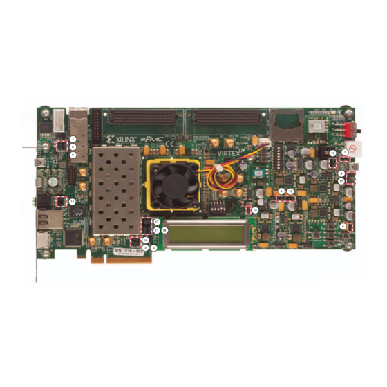
Page 10: Feature Descriptions
Chapter 1: VC707 Evaluation Board Features Feature Descriptions Figure 1-2 shows the VC707 board. Each numbered feature that is referenced in Figure 1-2 is described in the sections that follow. Note: The image in Figure 1-2 is for reference only and might not reflect the current revision of the board. - Page 11 Feature Descriptions Table 1-1: VC707 Board Component Descriptions (Cont’d) Schematic Reference 0381418 Callout Component Description Notes Designator Page Number C programmable user clock LVDS, Silicon Labs SI570BAB0000544DG 156.250 MHz default frequency (back side of board) J31, J32 User SMA clock...
-
Page 12: Virtex-7 Xc7Vx485T-2Ffg1761C Fpga
The VC707 board is populated with the Virtex-7 XC7VX485T-2FFG1761C FPGA. For further information on Virtex-7 FPGAs, see 7 Series FPGAs Overview (DS180) [Ref To determine the type of FPGA resident on the VC707 board, refer to the Master Answer Record listed in Appendix F: References. - Page 13 There are 17 I/O banks available on the Virtex-7 device. Sixteen I/O banks are available on the VC707 board, bank 31 is not used. The voltages applied to the FPGA I/O banks used by the VC707 board are listed in Table 1-3.
-
Page 14: Ddr3 Memory
Chapter 1: VC707 Evaluation Board Features DDR3 Memory [Figure 1-2, callout 2] The memory module at J1 is a 1 GB DDR3 small outline dual-inline memory module (SODIMM). It provides volatile synchronous dynamic random access memory (SDRAM) for storing user code and data. - Page 15 DQ18 DDR3_D19 DQ19 DDR3_D20 DQ20 DDR3_D21 DQ21 DDR3_D22 DQ22 DDR3_D23 DQ23 DDR3_D24 DQ24 DDR3_D25 DQ25 DDR3_D26 DQ26 DDR3_D27 DQ27 DDR3_D28 DQ28 DDR3_D29 DQ29 DDR3_D30 DQ30 DDR3_D31 DQ31 DDR3_D32 DQ32 VC707 Evaluation Board www.xilinx.com Send Feedback UG885 (v1.4) May 12, 2014...
- Page 16 Chapter 1: VC707 Evaluation Board Features Table 1-4: DDR3 Memory Connections to the FPGA (Cont’d) J1 DDR3 Memory FPGA (U1) Net Name Pin Number Pin Name DDR3_D33 DQ33 DDR3_D34 DQ34 DDR3_D35 DQ35 DDR3_D36 DQ36 DDR3_D37 DQ37 DDR3_D38 DQ38 DDR3_D39 DQ39...
- Page 17 DQS5_N DDR3_DQS5_P DQS5_P DDR3_DQS6_N DQS6_N DDR3_DQS6_P DQS6_P DDR3_DQS7_N DQS7_N DDR3_DQS7_P DQS7_P DDR3_ODT0 ODT0 DDR3_ODT1 ODT1 DDR3_RESET_B RESET_B DDR3_S0_B S0_B DDR3_S1_B S1_B DDR3_TEMP_EVENT EVENT_B DDR3_WE_B WE_B DDR3_CAS_B CAS_B DDR3_RAS_B RAS_B VC707 Evaluation Board www.xilinx.com Send Feedback UG885 (v1.4) May 12, 2014...
-
Page 18: Linear Bpi Flash Memory
CK1_N DDR3_CLK1_P CK1_P The VC707 DDR3 SODIMM interface adheres to the constraints guidelines in the DDR3 Design Guidelines section of 7 Series FPGAs Memory Interface Solutions User Guide (UG586) [Ref 3]. The VC707 DDR3 SODIMM interface is a 40Ω impedance implementation. Other... - Page 19 FLASH_A19 AT41 FLASH_A20 BA39 FLASH_A21 BA39 FLASH_A22 BB39 FLASH_A23 AW42 FLASH_A24 AW41 FLASH_A25 AM36 FLASH_D0 AN36 FLASH_D1 AJ36 FLASH_D2 AJ37 FLASH_D3 AK37 FLASH_D4 AL37 FLASH_D5 AN35 FLASH_D6 AP35 FLASH_D7 VC707 Evaluation Board www.xilinx.com Send Feedback UG885 (v1.4) May 12, 2014...
- Page 20 The configuration section of 7 Series FPGAs Configuration User Guide (UG470) [Ref 2] provides details on the Master BPI configuration mode. Figure 1-4 shows the connections of the linear BPI Flash memory on the VC707 board. For more details, see the Micron PC28F00AG18FE data sheet [Ref 16].
- Page 21 FLASH_WAIT_R FLASH_A23 WAIT FLASH_A24 FPGA_CCLK FLASH_A25 RFU1 VCCQ1 RFU2 VCCQ2 1.8V RFU3 VCCQ3 VSS0 VSS1 1.8V VCC1 VSS2 VSS3 VCC2 UG885_c1_04_021012 Figure 1-4: 128 MB Linear Flash Memory (U3) VC707 Evaluation Board www.xilinx.com Send Feedback UG885 (v1.4) May 12, 2014...
-
Page 22: Usb 2.0 Ulpi Transceiver
[Figure 1-2, callout 4] The VC707 board uses a Standard Microsystems Corporation USB3320 USB 2.0 ULPI Transceiver (U8) to support a USB connection to the host computer. A USB cable is supplied in the VC707 Evaluation Kit (type-A connector to host computer, mini-B connector to VC707 board connector J2). - Page 23 Table 1-7: USB 2.0 ULPI Transceiver Connections to the FPGA FPGA (U1) Pin Net Name USB3320 (U8) Pin AV36 USB_SMSC_DATA0 AW36 USB_SMSC_DATA1 BA34 USB_SMSC_DATA2 BB34 USB_SMSC_DATA3 BA36 USB_SMSC_DATA4 AT34 USB_SMSC_DATA5 VC707 Evaluation Board www.xilinx.com Send Feedback UG885 (v1.4) May 12, 2014...
-
Page 24: Sd Card Interface
[Figure 1-2, callout 5] The VC707 board includes a secure digital input/output (SDIO) interface to provide user-logic access to general purpose nonvolatile SDIO memory cards and peripherals. The SD card slot is designed to support 50 MHz high speed SD cards. -
Page 25: Usb Jtag
1-2, callout 6] JTAG configuration is provided through a Digilent onboard USB-to-JTAG configuration logic module (U26) where a host computer accesses the VC707 board JTAG chain through a type-A (host side) to micro-B (VC707 board side) USB cable. VC707 Evaluation Board www.xilinx.com... - Page 26 UG885_c1_07_021412 Figure 1-7: JTAG Chain Block Diagram When an FMC mezzanine card is attached to the VC707 board it is automatically added to the JTAG chain through electronically controlled single-pole single-throw (SPST) switches U27 and U28. The SPST switches are in a normally closed state and transition to an open state when an FMC mezzanine card is attached.
- Page 27 AG32 FMC1_PRSNT_M2C_B_LS AM31 VCC3V3 VCC1V8 VCC3V3 VCC1V8 SN74AVC1T45 Voltage Bank 0 SN74AVC2T45 Translator FPGA_TDI_BUF Voltage Translator FPGA_TMS_BUF FPGA_TCK_BUF VCC1V8 VCC3V3 JTAG_TDO SN74AVC1T45 Voltage Translator UG855_c1_08_021412 Figure 1-8: JTAG Circuit VC707 Evaluation Board www.xilinx.com Send Feedback UG885 (v1.4) May 12, 2014...
-
Page 28: Clock Generation
Chapter 1: VC707 Evaluation Board Features Clock Generation The VC707 board provides five clock sources for the FPGA. Table 1-9 lists the source devices for each clock. Table 1-9: VC707 Board Clock Sources Clock Clock Name Description Source System Clock SiT9102 2.5V LVDS 200 MHz Fixed Frequency Oscillator (SiTime). - Page 29 [Figure 1-2, callout 7] The VC707 board has a LVDS 200 MHz oscillator (U51) soldered onto the back side of the board and wired to an FPGA MRCC clock input on bank 38. This 200 MHz signal pair is named SYSCLK_P and SYSCLK_N, which are connected to FPGA U1 pins E19 and E18 respectively.
- Page 30 Chapter 1: VC707 Evaluation Board Features For more details, see the Silicon Labs Si570 data sheet [Ref 19]. The user clock circuit is shown in Figure 1-10. X-Ref Target - Figure 1-10 VCC3V3 VCC3V3 C192 0.01 μF 25V 4.7KΩ 5%...
- Page 31 [Figure 1-2, callout The VC707 board includes a pair of SMA connectors for a GTX clock wired to GTX Quad bank 113. This differential clock has signal names SMA_MGT_REFCLK_P and SMA_REFCLK_N, which are connected to FPGA U1 pins AK8 and AK7 respectively.
-
Page 32: Gtx Transceivers
The GTX transceivers in 7 series FPGAs are grouped into four channels described as Quads. The reference clock for a Quad can be sourced from the Quad above or Quad below the GTX Quad of interest. There are four GTX Quads on the VC707 board with connectivity as shown here: www.xilinx.com... - Page 33 GTX Interface Connections for FPGA U1 Transceiver Bank Net Name Connections MGT_BANK_113 GTXE2_CHANNEL_X1Y0 GTXE2_CHANNEL_X1Y1 SGMII GTXE2_CHANNEL_X1Y2 SFP+ GTXE2_CHANNEL_X1Y3 MGTREFCLK0 SGMII_CLK MGTREFCLK1 SMA_MGT_REFCLK MGT_BANK_114 GTXE2_CHANNEL_X1Y4 PCIe7 GTXE2_CHANNEL_X1Y5 PCIe6 GTXE2_CHANNEL_X1Y6 PCIe5 GTXE2_CHANNEL_X1Y7 PCIe4 MGTREFCLK0 Si5324 MGTREFCLK1 VC707 Evaluation Board www.xilinx.com Send Feedback UG885 (v1.4) May 12, 2014...
- Page 34 Chapter 1: VC707 Evaluation Board Features Table 1-11: GTX Interface Connections for FPGA U1 (Cont’d) Transceiver Bank Net Name Connections MGT_BANK_115 GTXE2_CHANNEL_X1Y8 PCIe3 GTXE2_CHANNEL_X1Y9 PCIe2 GTXE2_CHANNEL_X1Y10 PCIe1 GTXE2_CHANNEL_X1Y11 PCIe0 MGTREFCLK0 MGTREFCLK1 PCIe_CLK MGT_BANK_116 GTXE2_CHANNEL_X1Y12 FMC2 HPC DP4 GTXE2_CHANNEL_X1Y13 FMC2 HPC DP5...
-
Page 35: Pci Express Endpoint Connectivity
85Ω ±10%. The PCIe clock is routed as a 100Ω differential pair. The 7 series FPGAs GTX transceivers are used for multi-gigabit per second serial interfaces. The XC7VX485T-2FFG1761C FPGA (-2 speed grade) included with the VC707 board supports up to Gen2 x8. - Page 36 Chapter 1: VC707 Evaluation Board Features Table 1-12: PCIe Edge Connector Connections GTX Quad 115 (Cont’d) PCIe Edge Connector (P1) FPGA (U1) FHG1761 Net Name Function Placement Name PCIE_RX3_N PETn3 Integrated Endpoint block receive pair GTXE2_CHANNEL_X1Y8 PCIE_RX4_P PETp4 Integrated Endpoint block receive pair...
- Page 37 Pin Name Placement Pin Name MGTXTXP0_114_AK4 PCIE_TX7_P PERp7 GTXE2_CHANNEL_X1Y4 PCIE_TX7_N PERn7 GTXE2_CHANNEL_X1Y4 MGTXTXN0_114_AK3 MGTXRXP0_114_AG6 PCIE_RX7_P PETp7 GTXE2_CHANNEL_X1Y4 MGTXRXN0_114_AG5 PCIE_RX7_N PETn7 GTXE2_CHANNEL_X1Y4 PCIE_TX6_P PERp6 GTXE2_CHANNEL_X1Y5 MGTXTXP1_114_AJ2 MGTXTXN1_114_AJ1 PCIE_TX6_N PERn6 GTXE2_CHANNEL_X1Y5 VC707 Evaluation Board www.xilinx.com Send Feedback UG885 (v1.4) May 12, 2014...
- Page 38 Chapter 1: VC707 Evaluation Board Features Table 1-14: GTX Quad 114 PCIe Edge Connector Connections (Cont’d) PCIe Edge Connector (P1) Quad 114 FPGA (U1) FHG1761 Net Name PCIe Edge Pin Name Placement Pin Name PCIE_RX6_P PETp6 GTXE2_CHANNEL_X1Y5 MGTXRXP1_114_AF4 PCIE_RX6_N PETn6...
-
Page 39: Sfp/Sfp+ Module Connector
Feature Descriptions SFP/SFP+ Module Connector [Figure 1-2, callout 14] The VC707 board contains a small form-factor pluggable (SFP+) connector and cage assembly P3 that accepts SFP or SFP+ modules. Figure 1-16 shows the SFP+ module connector circuitry. X-Ref Target - Figure 1-16... -
Page 40: 10/100/1000 Tri-Speed Ethernet Phy
[Figure 1-2, callout 15] The VC707 board utilizes the Marvell Alaska PHY device (88E1111) U50 for Ethernet communications at 10, 100, or 1000 Mb/s. The board supports SGMII mode only. The PHY connection to a user-provided Ethernet cable is through a Halo HFJ11-1G01E RJ-45 connector (P4) with built-in magnetics. - Page 41 Table 1-18: Ethernet Connections, FPGA to PHY Device M88E1111 PHY U50 FPGA (U1) Net Name Name AK33 PHY_MDIO MDIO AH31 PHY_MDC AL31 PHY_INT INT_B AJ33 PHY_RESET RESET_B SGMII_TX_P SIN_P SGMII_TX_N SIN_N SGMII_RX_P SOUT_P SGMII_RX_N SOUT_N VC707 Evaluation Board www.xilinx.com Send Feedback UG885 (v1.4) May 12, 2014...
-
Page 42: Sgmii Gtx Transceiver Clock Generation
USB port. The USB cable is supplied in the VC707 Evaluation Kit (Type-A end to host computer, Type mini-B end to VC707 board connector J17). The CP2103GM is powered by the USB 5V provided by the host PC when the USB cable is plugged into the USB port on the VC707 board. -
Page 43: Hdmi Video Output
HDMI Video Output [Figure 1-2, callout 18] The VC707 board provides a High-Definition Multimedia Interface (HDMI™) video output using the Analog Devices ADV7511KSTZ-P HDMI transmitter (U48). The HDMI output is provided on a Molex 500254-1927 HDMI type-A connector (P2). The ADV7511 is wired to support 1080P 60 Hz YCbCr and RGB video modes through 36-bit input data mapping. - Page 44 Chapter 1: VC707 Evaluation Board Features Figure 1-18 shows the HDMI codec circuit. X-Ref Target - Figure 1-18 VCC3V3 VADJ VCC2V5 R104 R106 2.43K 2.43K SIT8102 R105 1/10W 1/10W 12.00000 MHZ 2.43K 50PPM 1/10W ADV7511 HDMI_INT IIC_SCL_HDMI CEC_CLK IIC_SDA_HDMI HDMI_SPDIF_OUT...
- Page 45 HDMI_D16 AN24 HDMI_D17 AY24 HDMI_D18 BB22 HDMI_D19 BA22 HDMI_D20 BA25 HDMI_D21 AY25 HDMI_D22 AY22 HDMI_D23 AY23 HDMI_D24 AV24 HDMI_D25 AU24 HDMI_D26 AW21 HDMI_D27 AV21 HDMI_D28 AT24 HDMI_D29 AR24 HDMI_D30 VC707 Evaluation Board www.xilinx.com Send Feedback UG885 (v1.4) May 12, 2014...
- Page 46 Chapter 1: VC707 Evaluation Board Features Table 1-21: FPGA to HDMI Codec Connections (ADV7511) (Cont’d) ADV7511 (U48) FPGA (U1) Pin Schematic Net Name Pin Number Pin Name AU21 HDMI_D31 AT21 HDMI_D32 AW22 HDMI_D33 AW23 HDMI_D34 AV23 HDMI_D35 AP21 HDMI_DE AR23...
-
Page 47: Lcd Character Display (16 X 2)
Feature Descriptions LCD Character Display (16 x 2) [Figure 1-2, callout 19] A 2-line by 16-character display is provided on the VC707 board (Figure 1-19). X-Ref Target - Figure 1-19 LCD Display (16 x 2) UG885_c1_19_020612 Figure 1-19: LCD Display The character display runs at 5.0V and is connected to the FPGA's 1.8V HP bank 15... -
Page 48: I 2 C Bus
Chapter 1: VC707 Evaluation Board Features The VC707 board base board uses a male Samtec MTLW-107-07-G-D-265 2x7 header (J23) with 0.025-inch square posts on 0.100-inch centers for connecting to a Samtec SLW-107-01-L-D female socket on the LCD display panel assembly. The LCD header... - Page 49 Feature Descriptions The VC707 board I C bus topology is shown in Figure 1-22. X-Ref Target - Figure 1-22 PCA9548 1 2 C 1-to-8 Bus Switch CH0 - USER_CLK_SDL/SCL CH1 - FMC1_HPC_IIC_SDA/SCL FPGA Bank 15 CH2 - FMC2_HPC_IIC_SDA/SCL (2.5V) CH3 - EEPROM_IIC_SDA/SCL...
-
Page 50: Status Leds
TPS51200 Power Good (U23) User I/O [Figure 1-2, callout - 26] The VC707 board provides the following user and general purpose I/O capabilities: • Eight user LEDs (callout 22) • GPIO_LED_[7-0]: DS9, DS8, DS7, DS6, DS5, DS4, DS3, DS2 •... - Page 51 Figure 1-23: User LEDs CPU Reset Pushbutton Figure 1-24 shows the CPU reset pushbutton switch circuit. X-Ref Target - Figure 1-24 CPU_RESET 4.7kΩ 0.1W UG885_c1_123_012513 Figure 1-24: CPU Reset Pushbutton VC707 Evaluation Board www.xilinx.com Send Feedback UG885 (v1.4) May 12, 2014...
- Page 52 Chapter 1: VC707 Evaluation Board Features User Pushbuttons Figure 1-25 shows the user pushbutton switch circuits. X-Ref Target - Figure 1-25 VCC1V8 GPIO SW N 4.7kΩ 0.1 W VCC1V8 VADJ VCC1V8 GPIO SW W GPIO SW C GPIO SW E 4.7kΩ...
- Page 53 X-Ref Target - Figure 1-27 Edge Drive Jog Encoder EVQ-WK4001 ROTARY INCB ROTARY PUSH SW1B SW1A ROTARY INCA SW10 4.7K 4.7K 4.7K 1/10W 1/10W 1/10W UG885_c1_125_012413 Figure 1-27: User Rotary Switch VC707 Evaluation Board www.xilinx.com Send Feedback UG885 (v1.4) May 12, 2014...
- Page 54 Chapter 1: VC707 Evaluation Board Features User SMA Figure 1-28 shows the user SMA circuit. X-Ref Target - Figure 1-28 USER SMA GPIO P Connector USER SMA GPIO N Connector UG885_c1_126_012413 Figure 1-28: User SMA Table 1-26 lists the GPIO Connections to FPGA U1.
-
Page 55: Switches
[Figure 1-2, callout 27] The VC707 board power switch is SW12. Sliding the switch actuator from the Off to On position applies 12V power from J18, a 6-pin mini-fit connector. Green LED DS16 illuminates when the VC707 board power is on. See... - Page 56 The VC707 Evaluation Kit provides the adapter cable shown in Figure 1-29 for powering the VC707 board from the ATX power supply 4-pin peripheral connector. The Xilinx part number for this cable is 2600304, and is equivalent to Sourcegate Technologies part number AZCBL-WH-1109-RA4.
- Page 57 R337 1.21kΩ 1.21kΩ 1.21kΩ 0.1 W 0.1 W 0.1 W R340 R338 1.21kΩ 1.21kΩ 0.1 W 0.1 W UG885_c1_29_030512 Figure 1-32: Configuration Mode and Upper Linear Flash Address Switch VC707 Evaluation Board www.xilinx.com Send Feedback UG885 (v1.4) May 12, 2014...
-
Page 58: Vita 57.1 Fmc1 Hpc Connector (Partially Populated)
The FMC1 HPC signals are distributed across GTX Quads 118 and 119. Each Quad has the VCCO voltage connected to VADJ. Note: The VC707 board VADJ voltage for the FMC1 HPC (J35) connector is determined by the FMC VADJ power sequencing logic described in FMC_VADJ Voltage Control, page VITA 57.1 FMC2 HPC Connector (Partially Populated) - Page 59 The FMC2 HPC signals are distributed across GTX Quads 116 and 117. Each Quad has the VCCO voltage connected to VADJ. Note: The VC707 board VADJ voltage for the FMC2 HPC (J37) connector is determined by the FMC VADJ power sequencing logic described in FMC_VADJ Voltage Control, page Signaling Speed Ratings: •...
- Page 60 Chapter 1: VC707 Evaluation Board Features Table 1-27 lists the connections between the FMC1 HPC J35 connector and the FPGA U1. Table 1-27: J35 VITA 57.1 FMC 1 HPC Connections U1 FPGA U1 FPGA FMC 1 Schematic Net Name FMC 1...
- Page 61 FMC1_HPC_LA13_N FMC1_HPC_LA18_CC_N FMC1_HPC_LA17_CC_P FMC1_HPC_LA27_P FMC1_HPC_LA17_CC_N FMC1_HPC_LA27_N FMC1_HPC_LA23_P FMC1_HPC_IIC_SCL U52.4 FMC1_HPC_LA23_N FMC1_HPC_IIC_SDA U52.3 FMC1_HPC_LA26_P FMC1_HPC_LA26_N VCC12_P FMC1_HPC_TCK_BUF U19.14 VCC12_P FMC_TDI_BUF U19.18 VCC3V3 FMC1_TDO_FMC2_TDI U27.2 VCC3V3 FMC1_HPC_TMS_BUF U19.17 VCC3V3 VCC3V3 VCC3V3 VC707 Evaluation Board www.xilinx.com Send Feedback UG885 (v1.4) May 12, 2014...
- Page 62 Chapter 1: VC707 Evaluation Board Features Table 1-27: J35 VITA 57.1 FMC 1 HPC Connections (Cont’d) U1 FPGA U1 FPGA FMC 1 Schematic Net Name FMC 1 Schematic Net Name HPC Pin HPC Pin FMC1_HPC_HA01_CC_P FMC1_HPC_PG_M2C AN34 FMC1_HPC_HA01_CC_N FMC1_HPC_HA00_CC_P FMC1_HPC_HA05_P...
- Page 63 FMC1_HPC_LA11_N FMC1_HPC_LA20_P FMC1_HPC_LA15_P FMC1_HPC_LA20_N FMC1_HPC_LA15_N FMC1_HPC_LA22_P FMC1_HPC_LA19_P FMC1_HPC_LA22_N FMC1_HPC_LA19_N FMC1_HPC_LA25_P FMC1_HPC_LA21_P FMC1_HPC_LA25_N FMC1_HPC_LA21_N FMC1_HPC_LA29_P FMC1_HPC_LA24_P FMC1_HPC_LA29_N FMC1_HPC_LA24_N FMC1_HPC_LA31_P FMC1_HPC_LA28_P FMC1_HPC_LA31_N FMC1_HPC_LA28_N FMC1_HPC_LA33_P FMC1_HPC_LA30_P FMC1_HPC_LA33_N FMC1_HPC_LA30_N VADJ FMC1_HPC_LA32_P FMC1_HPC_LA32_N VADJ VC707 Evaluation Board www.xilinx.com Send Feedback UG885 (v1.4) May 12, 2014...
- Page 64 Chapter 1: VC707 Evaluation Board Features Table 1-27: J35 VITA 57.1 FMC 1 HPC Connections (Cont’d) U1 FPGA U1 FPGA FMC 1 Schematic Net Name FMC 1 Schematic Net Name HPC Pin HPC Pin FMC1_HPC_HA03_P FMC1_HPC_HA03_N FMC1_HPC_HA02_P FMC1_HPC_HA07_P FMC1_HPC_HA02_N FMC1_HPC_HA07_N...
- Page 65 FMC2 HPC J37 connector and the FPGA U1. Note: The FMC2 HPC HB00-HB21 pair connections are not available with the XC7VX485T-2FFG1761C FPGA installed on the VC707. Refer to the Virtex-7 FPGA VC707 Evaluation Kit Master Answer Record in Appendix References for more information.
- Page 66 Chapter 1: VC707 Evaluation Board Features Table 1-28: J37 VITA 57.1 FMC 2 HPC Connections (Cont’d) J37 FMC 2 U1 FPGA J37 FMC 2 Schematic Net Name Schematic Net Name U1 FPGA Pin HPC Pin HPC Pin FMC2_HPC_LA14_P AB38 FMC2_HPC_LA09_N...
- Page 67 FMC2_HPC_LA07_P AC40 FMC2_HPC_LA12_N AA39 FMC2_HPC_LA07_N AC41 FMC2_HPC_LA16_P AJ40 FMC2_HPC_LA11_P FMC2_HPC_LA16_N AJ41 FMC2_HPC_LA11_N AA42 FMC2_HPC_LA20_P FMC2_HPC_LA15_P AC38 FMC2_HPC_LA20_N FMC2_HPC_LA15_N AC39 FMC2_HPC_LA22_P FMC2_HPC_LA19_P FMC2_HPC_LA22_N FMC2_HPC_LA19_N FMC2_HPC_LA25_P FMC2_HPC_LA21_P FMC2_HPC_LA25_N FMC2_HPC_LA21_N FMC2_HPC_LA29_P FMC2_HPC_LA24_P VC707 Evaluation Board www.xilinx.com Send Feedback UG885 (v1.4) May 12, 2014...
- Page 68 Chapter 1: VC707 Evaluation Board Features Table 1-28: J37 VITA 57.1 FMC 2 HPC Connections (Cont’d) J37 FMC 2 U1 FPGA J37 FMC 2 Schematic Net Name Schematic Net Name U1 FPGA Pin HPC Pin HPC Pin FMC2_HPC_LA29_N FMC2_HPC_LA24_N FMC2_HPC_LA31_P...
-
Page 69: Power Management
FMC2_VIO_B_M2C BANK 32 VCCO VCCO Power Management The VC707 board power distribution diagram is shown in Figure 1-33. The PCB layout and power system meet the recommended criteria described in 7 Series FPGAs PCB Design and Pin Planning Guide (UG483) - Page 70 Chapter 1: VC707 Evaluation Board Features X-Ref Target - Figure 1-33 VCC12_P Power Plane Power Controller 1 (Core) From SW12 PMBus Address 52 Switching Regulator VCCINT 1.0V at 20A VCCAUX Switching Regulator 1.8V at 20A Switching Regulator VCC3V3 3.3V at 10A...
- Page 71 Feature Descriptions The VC707 board uses power regulators and PMBus compliant digital PWM system controllers from Texas Instruments to supply the core and auxiliary voltages listed in Table 1-29. Table 1-29: Onboard Power System Devices Reference Power Rail Power Rail...
- Page 72 1-34. FMC_VADJ Voltage Control The FMC_VADJ rail is set to 1.8V. When the VC707 board is powered on, the state of the FMC_VADJ_ON_B signal wired to header J51 is sampled by the TI UCD9248 controller U42. If a jumper is installed on J51 signal FMC_VADJ_ON_B is held low, and the TI controller U42 energizes the FMC_VADJ rail at power on.
- Page 73 1.38 10.41 Notes: 1. The values defined in these columns are the voltage, current, and temperature thresholds that causes the regulator to shut down if the value is exceeded. VC707 Evaluation Board www.xilinx.com Send Feedback UG885 (v1.4) May 12, 2014...
- Page 74 24]. PCIe Form Factor Board TI Power System Cooling If the power modules on the VC707 board are operating at moderate to high current levels (due to a customer design), the modules can generate substantial heat, which can cause them to shut down without warning. The power module shutdown then turns off the FPGA on the development board.
-
Page 75: Xadc Analog-To-Digital Converter
UG885_c1_31_030512 Figure 1-34: XADC Block Diagram The VC707 board supports both the internal FPGA sensor measurements and the external measurement capabilities of the XADC. Internal measurements of the die temperature, VCCINT, VCCAUX, and VCCBRAM are available. The VC707 board VCCINT and VCCBRAM are provided by a common 1.0 V supply. - Page 76 Chapter 1: VC707 Evaluation Board Features For external measurements an XADC header (J19) is provided. This header can be used to provide analog inputs to the FPGA's dedicated VP/VN channel, and to the VAUXP[0]/VAUXN[0], VAUXP[8]/VAUXN[8] auxiliary analog input channels. Simultaneous sampling of Channel 0 and Channel 8 is supported.
-
Page 77: Configuration Options
Configuration Options Configuration Options The FPGA on the VC707 board can be configured by the following methods: • Master BPI (uses the Linear BPI Flash). • JTAG (uses the USB-to-JTAG Bridge or Download cable). See USB JTAG, page 25 more information... - Page 78 Chapter 1: VC707 Evaluation Board Features over the 16-bit datapath from the Linear BPI Flash memory at a maximum synchronous read rate of 80 MHz. X-Ref Target - Figure 1-37 FPGA VCCAUXIO (2.0V) PROG_B VBATT Part of Bank 0 BAS40-04 SW11 (VCCO = 1.8V)
-
Page 79: Appendix A: Default Switch And Jumper Settings
2 3 4 5 6 7 8 OFF Position = 0 UG885_aB_01_020612 Figure A-1: SW2 Default Settings Table A-1: SW2 Default Switch Settings Position Function Default GPIO_DIP_SW0 GPIO_DIP_SW1 GPIO_DIP_SW2 GPIO_DIP_SW3 GPIO_DIP_SW4 GPIO_DIP_SW5 GPIO_DIP_SW6 GPIO_DIP_SW7 VC707 Evaluation Board www.xilinx.com Send Feedback UG885 (v1.4) May 12, 2014... -
Page 80: Configuration Dip Switch Sw11
SFP RX Rate: 1-2 = Full BW Rate, 2-3 = Low BW Rate 1–2 SFP TX Rate: 1-2 = Full BW Rate, 2-3 = Low BW Rate 1–2 XADC external 1.2V or internal VREFP selector 1–2 www.xilinx.com VC707 Evaluation Board Send Feedback UG885 (v1.4) May 12, 2014... - Page 81 PCIe Bus Width Select Header TI Controller U64 Addr 54 Reset jumper None FMC_VADJ_ON_B jumper 1–2 FPGA U1 INIT_B-to-PROG_B jumper None XADC VCC5V0-to-XADC_VCC5V0 jumper 1–2 XADC REF3012 U35 V Select 1–2 VC707 Evaluation Board www.xilinx.com Send Feedback UG885 (v1.4) May 12, 2014...
- Page 82 Appendix A: Default Switch and Jumper Settings www.xilinx.com VC707 Evaluation Board Send Feedback UG885 (v1.4) May 12, 2014...
-
Page 83: Appendix B: Vita 57.1 Fmc Connector Pinouts
HB18_N LA32_P LA33_N HB20_P HB21_N 12P0V DP6_C2M_N HB17_N_CC LA32_N HB20_N 3P3V DP5_C2M_P VIO_B_M2C VADJ VADJ 3P3V DP5_C2M_N VIO_B_M2C VADJ VADJ 3P3V RES0 UG885_aC_01_020612 Figure B-1: FMC1 HPC Connector Pinout VC707 Evaluation Board www.xilinx.com Send Feedback UG885 (v1.4) May 12, 2014... - Page 84 HB18_N LA32_P LA33_N HB20_P HB21_N 12P0V DP6_C2M_N HB17_N_CC LA32_N HB20_N 3P3V DP5_C2M_P VIO_B_M2C VADJ VADJ 3P3V DP5_C2M_N VIO_B_M2C VADJ VADJ 3P3V RES0 UG885_aC_02_020612 Figure B-2: FMC2 HPC Connector Pinout www.xilinx.com VC707 Evaluation Board Send Feedback UG885 (v1.4) May 12, 2014...
-
Page 85: Appendix C: Master Constraints File Listing
The VC707 board master Xilinx design constraints (XDC) file template provides for designs targeting the VC707 board. Net names in the constraints listed in this appendix correlate with net names on the latest VC707 board schematic. Users must identify the appropriate pins and replace the net names listed here with net names in the user RTL. - Page 86 PACKAGE_PIN AT41 [get_ports FLASH_A20] set_property IOSTANDARD LVCMOS18 [get_ports FLASH_A20] set_property PACKAGE_PIN BA40 [get_ports FLASH_A21] set_property IOSTANDARD LVCMOS18 [get_ports FLASH_A21] set_property PACKAGE_PIN BA39 [get_ports FLASH_A22] set_property IOSTANDARD LVCMOS18 [get_ports FLASH_A22] www.xilinx.com VC707 Evaluation Board Send Feedback UG885 (v1.4) May 12, 2014...
- Page 87 VC707 Board XDC Listing set_property PACKAGE_PIN BB39 [get_ports FLASH_A23] set_property IOSTANDARD LVCMOS18 [get_ports FLASH_A23] set_property PACKAGE_PIN AW42 [get_ports FLASH_A24] set_property IOSTANDARD LVCMOS18 [get_ports FLASH_A24] set_property PACKAGE_PIN AW41 [get_ports FLASH_A25] set_property IOSTANDARD LVCMOS18 [get_ports FLASH_A25] set_property PACKAGE_PIN AY37 [get_ports FLASH_ADV_B] set_property IOSTANDARD LVCMOS18 [get_ports FLASH_ADV_B]...
- Page 88 PACKAGE_PIN AP3 [get_ports SMA_MGT_TX_N] set_property PACKAGE_PIN AN5 [get_ports SMA_MGT_RX_N] set_property PACKAGE_PIN E10 [get_ports FMC1_HPC_GBTCLK1_M2C_C_P] set_property PACKAGE_PIN E9 [get_ports FMC1_HPC_GBTCLK1_M2C_C_N] set_property PACKAGE_PIN A10 [get_ports FMC1_HPC_GBTCLK0_M2C_C_P] set_property PACKAGE_PIN A9 [get_ports FMC1_HPC_GBTCLK0_M2C_C_N] www.xilinx.com VC707 Evaluation Board Send Feedback UG885 (v1.4) May 12, 2014...
- Page 89 VC707 Board XDC Listing set_property PACKAGE_PIN T8 [get_ports FMC2_HPC_GBTCLK1_M2C_C_P] set_property PACKAGE_PIN T7 [get_ports FMC2_HPC_GBTCLK1_M2C_C_N] set_property PACKAGE_PIN K8 [get_ports FMC2_HPC_GBTCLK0_M2C_C_P] set_property PACKAGE_PIN K7 [get_ports FMC2_HPC_GBTCLK0_M2C_C_N] #FMC1 set_property PACKAGE_PIN L39 [get_ports FMC1_HPC_CLK0_M2C_P] set_property IOSTANDARD LVCMOS18 [get_ports FMC1_HPC_CLK0_M2C_P] set_property PACKAGE_PIN L40 [get_ports FMC1_HPC_CLK0_M2C_N]...
- Page 90 PACKAGE_PIN N39 [get_ports FMC1_HPC_LA14_P] set_property IOSTANDARD LVCMOS18 [get_ports FMC1_HPC_LA14_P] set_property PACKAGE_PIN N40 [get_ports FMC1_HPC_LA14_N] set_property IOSTANDARD LVCMOS18 [get_ports FMC1_HPC_LA14_N] set_property PACKAGE_PIN M36 [get_ports FMC1_HPC_LA15_P] set_property IOSTANDARD LVCMOS18 [get_ports FMC1_HPC_LA15_P] www.xilinx.com VC707 Evaluation Board Send Feedback UG885 (v1.4) May 12, 2014...
- Page 91 VC707 Board XDC Listing set_property PACKAGE_PIN L37 [get_ports FMC1_HPC_LA15_N] set_property IOSTANDARD LVCMOS18 [get_ports FMC1_HPC_LA15_N] set_property PACKAGE_PIN K37 [get_ports FMC1_HPC_LA16_P] set_property IOSTANDARD LVCMOS18 [get_ports FMC1_HPC_LA16_P] set_property PACKAGE_PIN K38 [get_ports FMC1_HPC_LA16_N] set_property IOSTANDARD LVCMOS18 [get_ports FMC1_HPC_LA16_N] set_property PACKAGE_PIN L31 [get_ports FMC1_HPC_LA17_CC_P] set_property IOSTANDARD LVCMOS18 [get_ports FMC1_HPC_LA17_CC_P]...
- Page 92 PACKAGE_PIN E32 [get_ports FMC1_HPC_HA09_P] set_property IOSTANDARD LVCMOS18 [get_ports FMC1_HPC_HA09_P] set_property PACKAGE_PIN D32 [get_ports FMC1_HPC_HA09_N] set_property IOSTANDARD LVCMOS18 [get_ports FMC1_HPC_HA09_N] set_property PACKAGE_PIN H38 [get_ports FMC1_HPC_HA10_P] set_property IOSTANDARD LVCMOS18 [get_ports FMC1_HPC_HA10_P] www.xilinx.com VC707 Evaluation Board Send Feedback UG885 (v1.4) May 12, 2014...
- Page 93 VC707 Board XDC Listing set_property PACKAGE_PIN G38 [get_ports FMC1_HPC_HA10_N] set_property IOSTANDARD LVCMOS18 [get_ports FMC1_HPC_HA10_N] set_property PACKAGE_PIN J37 [get_ports FMC1_HPC_HA11_P] set_property IOSTANDARD LVCMOS18 [get_ports FMC1_HPC_HA11_P] set_property PACKAGE_PIN J38 [get_ports FMC1_HPC_HA11_N] set_property IOSTANDARD LVCMOS18 [get_ports FMC1_HPC_HA11_N] set_property PACKAGE_PIN B37 [get_ports FMC1_HPC_HA12_P] set_property IOSTANDARD LVCMOS18 [get_ports FMC1_HPC_HA12_P]...
- Page 94 PACKAGE_PIN J21 [get_ports FMC1_HPC_HB14_P] set_property IOSTANDARD LVCMOS18 [get_ports FMC1_HPC_HB14_P] set_property PACKAGE_PIN H21 [get_ports FMC1_HPC_HB14_N] set_property IOSTANDARD LVCMOS18 [get_ports FMC1_HPC_HB14_N] set_property PACKAGE_PIN M21 [get_ports FMC1_HPC_HB15_P] set_property IOSTANDARD LVCMOS18 [get_ports FMC1_HPC_HB15_P] www.xilinx.com VC707 Evaluation Board Send Feedback UG885 (v1.4) May 12, 2014...
- Page 95 VC707 Board XDC Listing set_property PACKAGE_PIN L21 [get_ports FMC1_HPC_HB15_N] set_property IOSTANDARD LVCMOS18 [get_ports FMC1_HPC_HB15_N] set_property PACKAGE_PIN N25 [get_ports FMC1_HPC_HB16_P] set_property IOSTANDARD LVCMOS18 [get_ports FMC1_HPC_HB16_P] set_property PACKAGE_PIN N26 [get_ports FMC1_HPC_HB16_N] set_property IOSTANDARD LVCMOS18 [get_ports FMC1_HPC_HB16_N] set_property PACKAGE_PIN M24 [get_ports FMC1_HPC_HB17_CC_P] set_property IOSTANDARD LVCMOS18 [get_ports FMC1_HPC_HB17_CC_P]...
- Page 96 PACKAGE_PIN AK38 [get_ports FMC2_HPC_LA09_N] set_property IOSTANDARD LVCMOS18 [get_ports FMC2_HPC_LA09_N] set_property PACKAGE_PIN AB41 [get_ports FMC2_HPC_LA10_P] set_property IOSTANDARD LVCMOS18 [get_ports FMC2_HPC_LA10_P] set_property PACKAGE_PIN AB42 [get_ports FMC2_HPC_LA10_N] set_property IOSTANDARD LVCMOS18 [get_ports FMC2_HPC_LA10_N] www.xilinx.com VC707 Evaluation Board Send Feedback UG885 (v1.4) May 12, 2014...
- Page 97 VC707 Board XDC Listing set_property PACKAGE_PIN Y42 [get_ports FMC2_HPC_LA11_P] set_property IOSTANDARD LVCMOS18 [get_ports FMC2_HPC_LA11_P] set_property PACKAGE_PIN AA42 [get_ports FMC2_HPC_LA11_N] set_property IOSTANDARD LVCMOS18 [get_ports FMC2_HPC_LA11_N] set_property PACKAGE_PIN Y39 [get_ports FMC2_HPC_LA12_P] set_property IOSTANDARD LVCMOS18 [get_ports FMC2_HPC_LA12_P] set_property PACKAGE_PIN AA39 [get_ports FMC2_HPC_LA12_N] set_property IOSTANDARD LVCMOS18 [get_ports FMC2_HPC_LA12_N]...
- Page 98 PACKAGE_PIN AC29 [get_ports FMC2_HPC_HA04_N] set_property IOSTANDARD LVCMOS18 [get_ports FMC2_HPC_HA04_N] set_property PACKAGE_PIN Y32 [get_ports FMC2_HPC_HA05_P] set_property IOSTANDARD LVCMOS18 [get_ports FMC2_HPC_HA05_P] set_property PACKAGE_PIN Y33 [get_ports FMC2_HPC_HA05_N] set_property IOSTANDARD LVCMOS18 [get_ports FMC2_HPC_HA05_N] www.xilinx.com VC707 Evaluation Board Send Feedback UG885 (v1.4) May 12, 2014...
- Page 99 VC707 Board XDC Listing set_property PACKAGE_PIN AB31 [get_ports FMC2_HPC_HA06_P] set_property IOSTANDARD LVCMOS18 [get_ports FMC2_HPC_HA06_P] set_property PACKAGE_PIN AB32 [get_ports FMC2_HPC_HA06_N] set_property IOSTANDARD LVCMOS18 [get_ports FMC2_HPC_HA06_N] set_property PACKAGE_PIN AC31 [get_ports FMC2_HPC_HA07_P] set_property IOSTANDARD LVCMOS18 [get_ports FMC2_HPC_HA07_P] set_property PACKAGE_PIN AD31 [get_ports FMC2_HPC_HA07_N] set_property IOSTANDARD LVCMOS18 [get_ports FMC2_HPC_HA07_N]...
- Page 100 PACKAGE_PIN AN21 [get_ports HDMI_R_D12] set_property IOSTANDARD LVCMOS18 [get_ports HDMI_R_D12] set_property PACKAGE_PIN AP22 [get_ports HDMI_R_D13] set_property IOSTANDARD LVCMOS18 [get_ports HDMI_R_D13] set_property PACKAGE_PIN AP23 [get_ports HDMI_R_D14] set_property IOSTANDARD LVCMOS18 [get_ports HDMI_R_D14] www.xilinx.com VC707 Evaluation Board Send Feedback UG885 (v1.4) May 12, 2014...
- Page 101 VC707 Board XDC Listing set_property PACKAGE_PIN AN23 [get_ports HDMI_R_D15] set_property IOSTANDARD LVCMOS18 [get_ports HDMI_R_D15] set_property PACKAGE_PIN AM23 [get_ports HDMI_R_D16] set_property IOSTANDARD LVCMOS18 [get_ports HDMI_R_D16] set_property PACKAGE_PIN AN24 [get_ports HDMI_R_D17] set_property IOSTANDARD LVCMOS18 [get_ports HDMI_R_D17] set_property PACKAGE_PIN AY24 [get_ports HDMI_R_D18] set_property IOSTANDARD LVCMOS18 [get_ports HDMI_R_D18]...
- Page 102 PACKAGE_PIN AN31 [get_ports USER_SMA_GPIO_P] set_property IOSTANDARD LVCMOS18 [get_ports USER_SMA_GPIO_P] set_property PACKAGE_PIN AP31 [get_ports USER_SMA_GPIO_N] set_property IOSTANDARD LVCMOS18 [get_ports USER_SMA_GPIO_N] set_property PACKAGE_PIN AJ32 [get_ports USER_SMA_CLOCK_P] set_property IOSTANDARD LVCMOS18 [get_ports USER_SMA_CLOCK_P] www.xilinx.com VC707 Evaluation Board Send Feedback UG885 (v1.4) May 12, 2014...
- Page 103 VC707 Board XDC Listing set_property PACKAGE_PIN AK32 [get_ports USER_SMA_CLOCK_N] set_property IOSTANDARD LVCMOS18 [get_ports USER_SMA_CLOCK_N] set_property PACKAGE_PIN AK34 [get_ports USER_CLOCK_P] set_property IOSTANDARD LVDS [get_ports USER_CLOCK_P] set_property PACKAGE_PIN AL34 [get_ports USER_CLOCK_N] set_property IOSTANDARD LVDS [get_ports USER_CLOCK_N] #FAN set_property PACKAGE_PIN BA37 [get_ports SM_FAN_PWM]...
- Page 104 PACKAGE_PIN L12 [get_ports DDR3_D7] set_property IOSTANDARD SSTL15 [get_ports DDR3_D7] set_property PACKAGE_PIN K14 [get_ports DDR3_D8] set_property IOSTANDARD SSTL15 [get_ports DDR3_D8] set_property PACKAGE_PIN K13 [get_ports DDR3_D9] set_property IOSTANDARD SSTL15 [get_ports DDR3_D9] www.xilinx.com VC707 Evaluation Board Send Feedback UG885 (v1.4) May 12, 2014...
- Page 105 VC707 Board XDC Listing set_property PACKAGE_PIN H13 [get_ports DDR3_D10] set_property IOSTANDARD SSTL15 [get_ports DDR3_D10] set_property PACKAGE_PIN J13 [get_ports DDR3_D11] set_property IOSTANDARD SSTL15 [get_ports DDR3_D11] set_property PACKAGE_PIN L16 [get_ports DDR3_D12] set_property IOSTANDARD SSTL15 [get_ports DDR3_D12] set_property PACKAGE_PIN L15 [get_ports DDR3_D13] set_property IOSTANDARD SSTL15 [get_ports DDR3_D13]...
- Page 106 PACKAGE_PIN K12 [get_ports DDR3_DQS1_P] set_property IOSTANDARD SSTL15 [get_ports DDR3_DQS1_P] set_property PACKAGE_PIN J12 [get_ports DDR3_DQS1_N] set_property IOSTANDARD SSTL15 [get_ports DDR3_DQS1_N] set_property PACKAGE_PIN H16 [get_ports DDR3_DQS2_P] set_property IOSTANDARD SSTL15 [get_ports DDR3_DQS2_P] www.xilinx.com VC707 Evaluation Board Send Feedback UG885 (v1.4) May 12, 2014...
- Page 107 VC707 Board XDC Listing set_property PACKAGE_PIN G16 [get_ports DDR3_DQS2_N] set_property IOSTANDARD SSTL15 [get_ports DDR3_DQS2_N] set_property PACKAGE_PIN C15 [get_ports DDR3_DQS3_P] set_property IOSTANDARD SSTL15 [get_ports DDR3_DQS3_P] set_property PACKAGE_PIN C14 [get_ports DDR3_DQS3_N] set_property IOSTANDARD SSTL15 [get_ports DDR3_DQS3_N] set_property PACKAGE_PIN A26 [get_ports DDR3_DQS4_P] set_property IOSTANDARD DIFF_SSTL15 [get_ports DDR3_DQS4_P]...
- Page 108 PACKAGE_PIN AT34 [get_ports USB_SMSC_DATA5] set_property IOSTANDARD LVCMOS18 [get_ports USB_SMSC_DATA5] set_property PACKAGE_PIN AY35 [get_ports USB_SMSC_DATA6] set_property IOSTANDARD LVCMOS18 [get_ports USB_SMSC_DATA6] set_property PACKAGE_PIN AW35 [get_ports USB_SMSC_DATA7] set_property IOSTANDARD LVCMOS18 [get_ports USB_SMSC_DATA7] www.xilinx.com VC707 Evaluation Board Send Feedback UG885 (v1.4) May 12, 2014...
-
Page 109: Appendix D: Board Setup
Installation of the VC707 board inside a computer chassis is required when developing or testing PCI Express functionality. When the VC707 board is used inside a computer chassis (that is, plugged in to the PCIe® slot), power is provided from the ATX power supply 4-pin peripheral connector through... - Page 110 Appendix D: Board Setup www.xilinx.com VC707 Evaluation Board Send Feedback UG885 (v1.4) May 12, 2014...
-
Page 111: Appendix E: Board Specifications
Board Specifications Dimensions Height 5.5 inch (14.0 cm) Length 10.5 inch (26.7 cm) Note: The VC707 board height exceeds the standard 4.376 inch (11.15 cm) height of a PCI Express card. Environmental Temperature Operating: 0°C to +45°C Storage: –25°C to +60°C... - Page 112 Appendix E: Board Specifications www.xilinx.com VC707 Evaluation Board Send Feedback UG885 (v1.4) May 12, 2014...
-
Page 113: Appendix F: Additional Resources
Topics include design assistance, advisories, and troubleshooting tips. References The most up to date information related to the VC707 board and its documentation is available on these websites: • Virtex-7 FPGA VC707 Evaluation Kit •... - Page 114 (ADV7511KSTZ-P) DisplayTech (S162DBABC LCD) Texas Instruments Fusion Tools Documentation, 24. Texas Instruments: Texas Instruments, Texas Instruments Digital Power & Interface Solutions (UCD9248PFC, PTD08A010W, PTD08A020W, PTD08D021W, LMZ12002, TL1962ADC, ADP123, TPS51200DR) www.xilinx.com VC707 Evaluation Board Send Feedback UG885 (v1.4) May 12, 2014...
-
Page 115: Appendix G: Regulatory And Compliance Information
This product is designed and tested to conform to the European Union directives and standards described in this section. See the Virtex-7 FPGA VC707 Evaluation Kit Answer Record (AR 45382) for information on the CE requirements for the PC test environment. -
Page 116: Markings
This product complies with Directive 2002/95/EC on the restriction of hazardous substances (RoHS) in electrical and electronic equipment. This product complies with CE Directives 2006/95/EC, Low Voltage Directive (LVD) and 2004/108/EC, Electromagnetic Compatibility (EMC) Directive. www.xilinx.com VC707 Evaluation Board Send Feedback UG885 (v1.4) May 12, 2014...
Need help?
Do you have a question about the VC707 and is the answer not in the manual?
Questions and answers