Advertisement
Quick Links
D
i
g
i
l
e
n
t
N
e
D
i
g
i
l
e
n
t
N
e
R
e
f
e
r
e
n
c
e
M
R
e
f
e
r
e
n
c
e
M
Revision: July 11, 2011
Overview
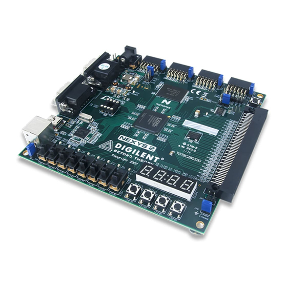
The Nexys2 circuit board is a complete,
ready-to-use circuit development platform
based on a Xilinx Spartan 3E FPGA. Its on-
board high-speed USB2 port, 16Mbytes of
RAM and ROM, and several I/O devices and
ports make it an ideal platform for digital
systems of all kinds, including embedded
processor systems based on Xilinx's
MicroBlaze. The USB2 port provides board
power and a programming interface, so the
Nexys2 board can be used with a notebook
computer to create a truly portable design
station.
The Nexys2 brings leading technologies to a
platform that anyone can use to gain digital
design experience. It can host countless
FPGA-based digital systems, and designs
can easily grow beyond the board using any
or all of the five expansion connectors. Four
12-pin Peripheral Module (Pmod) connectors
can accommodate up to eight low-cost
Pmods to add features like motor control, A/D
and D/A conversion, audio circuits, and a host
of sensor and actuator interfaces. All user-
accessible signals on the Nexys2 board are
ESD and short-circuit protected, ensuring a
long operating life in any environment.
The Nexys2 board is fully compatible with all
versions of the Xilinx ISE tools, including the
free WebPack. Now anyone can build real
digital systems for less than the price of a
textbook.
Power Supplies
The Nexys2 board input power input bus can be driven from a USB cable, from a 5VDC-15VDC,
center positive, 2.1mm wall-plug supply, or from a battery pack. A shorting block loaded on the
"power select" jumper selects the power source. The USB circuitry is always powered from the USB
cable – if no USB cable is attached, the USB circuitry is left unpowered.
Copyright Digilent, Inc. All rights reserved
x
y
s
2
B
o
a
r
d
x
y
s
2
B
o
a
r
d
a
n
u
a
l
a
n
u
a
l
215 E Main Suite D | Pullman, WA 99163
• 500K-gate Xilinx Spartan 3E FPGA
• USB2-based FPGA configuration and high-speed data
transfers (using the free Adept Suite Software)
• USB-powered (batteries and/or wall-plug can also be used)
• 16MB of Micron PSDRAM &16MB of Intel StrataFlash ROM
• Xilinx Platform Flash for nonvolatile FPGA configurations
• Efficient switch-mode power supplies (good for battery
powered applications)
• 50MHz oscillator plus socket for second oscillator
• 60 FPGA I/O's routed to expansion connectors (one high-
speed Hirose FX2 connector and four 6-pin headers)
• 8 LEDs, 4-digit 7-seg display, 4 buttons, 8 slide switches
• Ships in a plastic carry case with USB cable
Figure 1: Nexys2 block diagram and features
12 pages
ww w. d ig i l en t inc .c om
(509) 334 6306 Voice and Fax
Doc: 502-134
®
Advertisement

Related Manuals for Digilent Nexys2


Summary of Contents for Digilent Nexys2
- Page 1 Power Supplies The Nexys2 board input power input bus can be driven from a USB cable, from a 5VDC-15VDC, center positive, 2.1mm wall-plug supply, or from a battery pack. A shorting block loaded on the “power select” jumper selects the power source. The USB circuitry is always powered from the USB cable –...
- Page 2 IC5: LTC1844 150mA/60mA Technology. These regulators not only use USB power efficiently, they also allow the Nexys2 to run from battery packs for extended periods. Total board current depends on the FPGA configuration, clock frequency, and external connections. In test...
- Page 3 To program the Nexys2 board using Adept, attach the USB cable to the board (if USB power will not be used, attach a suitable power supply to the power jack or battery connector on the board, and set the power switch to “wall”...
- Page 4 Figure 6: Nexys2 clocks User I/O The Nexys2 board includes several input devices, output devices, and data ports, allowing many designs to be implemented without the need for any other components. Figure 7: Nexys2 board I/O devices Inputs: Slide Switches and Pushbuttons Four pushbuttons and eight slide switches are provided for circuit inputs.
- Page 5 -500 and the -1200 die. Outputs: Seven-Segment Display The Nexys2 board contains a four-digit common anode seven-segment LED display. Each of the four digits is composed of seven segments arranged in a “figure 8” pattern, with an LED embedded in each segment.
- Page 6 An un-illuminated seven-segment display, and nine illumination patterns corresponding to decimal digits Figure 9: Nexys2 seven-segment displays A scanning display controller circuit can be used to show a four-digit number on this display. This circuit drives the anode signals and corresponding cathode patterns of each digit in a repeating, continuous succession, at an update rate that is faster than the human eye can detect.
- Page 7 Digilent website. The USB port can also provide power to the Nexys2 board if the power select jumper is set to “USB”. The USB specification requires that attached devices draw no more than 100mA until they have requested more current, after which up to 500mA may be drawn.
- Page 8 Digilent Nexys2 Reference Manual www.digilentinc.com device can illuminate state LEDs on the keyboard). Bus timings are shown in the figure. The clock and data signals are only driven when data transfers occur, and otherwise they are held in the “idle”...
- Page 9 Digilent Nexys2 Reference Manual www.digilentinc.com Figure 14: PS/2 keyboard scan codes Mouse The mouse outputs a clock and data signal when it is moved; otherwise, these signals remain at logic ‘1’. Each time the mouse is moved, three 11-bit words are sent from the mouse to the host device.
-
Page 10: Vga System Timing
Nexys2 Reference Manual www.digilentinc.com VGA Port The Nexys2 board uses 10 FPGA signals to create a VGA port with 8-bit color and the two standard sync signals (HS – Horizontal Sync, and VS – Vertical Sync). The color signals use... -
Page 11: Display Surface
Digilent Nexys2 Reference Manual www.digilentinc.com from the cathodes, and those rays are fed by the current that flows into the cathodes. These particle rays are initially accelerated towards the grid, but they soon fall under the influence of the much larger electrostatic force that results from the entire phosphor-coated display surface of the CRT being charged to 20kV (or more). - Page 12 Nexys2 Reference Manual www.digilentinc.com more bytes assigned to each pixel location (the Nexys2 uses three bits per pixel). The controller must index into video memory as the beams move across the display, and retrieve and apply video data to the display at precisely the time the electron beam is moving across a given pixel.
- Page 13 Figure 21: Nexys2 serial port circuit Memory The Nexys2 board has external RAM and ROM devices. The external RAM is a 128Mbit Micron M45W8MW16 Cellular RAM pseudo-static DRAM device organized as 8Mbytes x 16bits. It can operate as a typical asynchronous SRAM with read and write cycle times of 70ns, or as a synchronous memory with an 80MHz bus.
- Page 14 Nexys2 Reference Manual www.digilentinc.com VDHL source code is available in a reference design posted on the Digilent website to illustrate the use of these devices. A base system builder file is also available for using these devices with Xilinx’s EDK tool and MicroBlaze processor core, both available from Xilinx. Complete information is available for both devices from the manufacturer websites.
-
Page 15: Peripheral Connectors
All data signals include short circuit protection resistors and ESD protection Diodes. A jumper block adjacent to each Pmod connector can connect the Pmod’s Vdd signal to the Nexys2 board’s 3.3V supply or to the input power bus (VU). If the jumper is set to VU and USB power is driving the main power bus, care should be taken to ensure no more than 200mA is consumed by the Pmod. -
Page 16: Expansion Connector
Expansion connector Table 4: Hirose FX2 Connector Pin Assignments Name FPGA Name FPGA The Nexys2 board includes a Hirose FX-2 high- VCC3V3 SHIELD density 100 pin connector that is suitable for VCC3V3 driving peripheral boards with signal rates in TDO-ROM excess of 100 MHz. - Page 17 ROM using the Adept programming software. All Nexys2 boards are 100% tested during the manufacturing process. If any device on the Nexys2 board fails test or is not responding properly, it is likely that damage occurred during transport or during use.
- Page 18 Mouser Electronics Authorized Distributor Click to View Pricing, Inventory, Delivery & Lifecycle Information: Digilent 410-134P-KIT...
Need help?
Do you have a question about the Nexys2 and is the answer not in the manual?
Questions and answers