Table of Contents
Advertisement
ZYBO™ FPGA Board Reference Manual
Revised April 11, 2016
This manual applies to the ZYBO rev. B
Overview
The ZYBO (ZYnq BOard) is a feature-rich, ready-to-use, entry-level embedded software and digital circuit
development platform built around the smallest member of the Xilinx Zynq-7000 family, the Z-7010. The Z-7010 is
based on the Xilinx All Programmable System-on-Chip (AP SoC) architecture, which tightly integrates a dual-core
ARM Cortex-A9 processor with Xilinx 7-series Field Programmable Gate Array (FPGA) logic. When coupled with the
rich set of multimedia and connectivity peripherals available on the ZYBO, the Zynq Z-7010 can host a whole
system design. The on-board memories, video and audio I/O, dual-role USB, Ethernet, and SD slot will have your
design up-and-ready with no additional hardware needed. Additionally, six Pmod ports are available to put any
design on an easy growth path.
The Zynq 7010 AP SoC offers the following features:
650Mhz dual-core Cortex-A9 processor
DDR3 memory controller with 8 DMA channels
High-bandwidth peripheral controllers: 1G Ethernet, USB 2.0, SDIO
Low-bandwidth peripheral controller: SPI, UART, CAN, I
Reprogrammable logic equivalent to Artix-7 FPGA
o
4,400 logic slices, each with four 6-input LUTs and 8 flip-flops
o
240 KB of fast block RAM
o
Two clock management tiles, each with a phase-locked loop (PLL) and mixed-mode clock
manager (MMCM)
o
80 DSP slices
o
Internal clock speeds exceeding 450MHz
o
On-chip analog-to-digital converter (XADC)
DOC#: 502-279
Other product and company names mentioned may be trademarks of their respective owners.
2
C
Copyright Digilent, Inc. All rights reserved.
1300 Henley Court
Pullman, WA 99163
509.334.6306
www.digilentinc.com
Page 1 of 26
Advertisement
Table of Contents

Related Manuals for Digilent ZYBO


Summary of Contents for Digilent ZYBO
- Page 1 ARM Cortex-A9 processor with Xilinx 7-series Field Programmable Gate Array (FPGA) logic. When coupled with the rich set of multimedia and connectivity peripherals available on the ZYBO, the Zynq Z-7010 can host a whole system design. The on-board memories, video and audio I/O, dual-role USB, Ethernet, and SD slot will have your design up-and-ready with no additional hardware needed.
- Page 2 This license is a 1 year, device-locked license, and will only work with the Z-7010 Zynq part on the ZYBO. After the license expires, any version of Vivado Design Suite that was released during this 1 year period can continue to be used indefinitely.
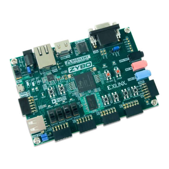
- Page 3 ZYBO™ FPGA Board Reference Manual Callout Component Description Callout Component Description Power Switch Processor Reset Pushbutton Power Select Jumper and battery header Logic configuration reset Pushbutton Shared UART/JTAG USB port Audio Codec Connectors MIO LED Logic Configuration Done LED MIO Pushbuttons (2)
-
Page 4: Power Supplies
ZYBO™ FPGA Board Reference Manual Power Supplies The ZYBO can be powered from the Digilent USB-JTAG-UART port (J11), or from an external power supply. Jumper JP7 (near the power switch) determines which power source is used. There are three valid configurations for this jumper corresponding to the three powering options: USB, wall wart with barrel jack, and battery pack. -
Page 5: Zynq Ap Soc Architecture
ZYBO™ FPGA Board Reference Manual Voltage regulator circuits from Analog Devices create the required 3.3V, 1.8V, 1.5V, and 1.0V supplies from the main power input. Table 2 provides additional information (typical currents depend strongly on FPGA configuration and the values provided are typical of medium size/speed designs). - Page 6 ZYBO™ FPGA Board Reference Manual Figure 3. Zynq AP SoC architecture. The PL is nearly identical to a Xilinx 7-series Artix FPGA, except that it contains several dedicated ports and buses that tightly couple it to the PS. The PL also does not contain the same configuration hardware as a typical 7-series FPGA, and it must be configured either directly by the processor or via the JTAG port.
- Page 7 Zynq Technical Reference Manual, available at www.xilinx.com. Figure 3 depicts the external components connected to the MIO pins of the ZYBO. The Zynq Board Definition File found on the Digilent ZYBO product page can be imported into EDK and Vivado Designs to properly configure the PS to work with these peripherals.
- Page 8 ZYBO™ FPGA Board Reference Manual MIO 501 Peripherals 1.8V ENET 0 USB 0 SDIO 0 UART 1 GPIO TXCK TXD0 TXD1 TXD2 TXD3 TXCTL RXCK RXD0 RXD1 RXD2 RXD3 RXCTL DATA4 DATA0 DATA1 DATA2 DATA3 DATA5 DATA6 DATA7 CCLK RESETN...
-
Page 9: Zynq Configuration
Zynq was just powered on, the BootROM will first latch the state of the mode pins into the mode register (the mode pins are attached to JP5 on the ZYBO). If the BootROM is being executed due to a reset event, then the mode pins are not latched, and the previous state of the mode register is used. - Page 10 QSPI Boot Mode The ZYBO has an onboard 128-Mbit Quad-SPI (QSPI) serial Flash that the Zynq can boot from. The ZYBO Base System Design includes a tutorial for how to configure the QSPI Flash with a Zynq Boot Image using the iMPACT tool included with Xilinx ISE and Vivado.
-
Page 11: Spi Flash
The ZYBO is configured to boot in Cascaded JTAG mode, which allows the PS to be accessed via the same JTAG port as the PL. It is also possible to boot the ZYBO in Independent JTAG mode by loading a jumper in JP6 and shorting it. -
Page 12: Usb Uart Bridge (Serial Port)
For more details on memory controller operation, refer to the Xilinx Zynq TRM (ug585). USB UART Bridge (Serial Port) The ZYBO includes an FTDI FT2232HQ USB-UART bridge (attached to connector J11) that lets you use PC applications to communicate with the board using standard Windows COM port commands. Free USB-COM port drivers, available from www.ftdichip.com under the "Virtual Com Port"... -
Page 13: Microsd Slot
MicroSD Slot The ZYBO provides a microSD slot (J4) for non-volatile external memory storage as well as booting the Zynq. The slot is wired to Bank 1/501 MIO[40-47], including Card Detect. On the PS side peripheral SDIO 0 is mapped out to these pins and controls communication with the SD card. -
Page 14: Ethernet Phy
While in host mode, the ZYBO is technically an "embedded host", because it does not provide the required 150 µF of capacitance on VBUS required to qualify as a general purpose host. It is possible to modify the ZYBO so that it complies with the general purpose USB host requirements by loading C64 with a 150 µF capacitor and shorting JP2. - Page 15 MIO bank is powered from 1.8V, the RGMII interface uses 1.8V HSTL Class 1 drivers. For this I/O standard an external reference of 0.9V is provided in bank 501 (PS_MIO_VREF). Mapping out the correct pins and configuring the interface is handled by the ZYBO board definition file. Copyright Digilent, Inc. All rights reserved.
-
Page 16: Hdmi Source/Sink Port
On an Ethernet network each node needs a unique MAC address. To this end, a Microchip 24AA02E48 EEPROM is provided on the ZYBO. On one hand it is a read-writeable EEPROM that can be accessed via I C. On the other hand it features a read-only memory section that comes pre-programmed with a unique identifier. - Page 17 HDMI specifications only require terminations on the Sink side, but optional Source-side terminations reduce reflections, resulting in improved signal quality. Do not connect powered HDMI/DVI devices to an unpowered ZYBO, as it might result in back-powering the board through the termination resistors. Resolutions up to 720p (1280x720) have been tested.
- Page 18 ZYBO™ FPGA Board Reference Manual 11.1 VGA System Timing VGA signal timings are specified, published, copyrighted, and sold by the VESA organization (www.vesa.org). The following VGA system timing information is provided as an example of how a VGA monitor might be driven in 640 by 480 mode.
- Page 19 Video data typically comes from a video refresh memory; with one or more bytes assigned to each pixel location (the ZYBO uses 16 bits per pixel). The controller must index into video memory as the beams move across the display, and retrieve and apply video data to the display at precisely the time the electron beam is moving across a given pixel.
- Page 20 ZYBO™ FPGA Board Reference Manual refresh frequencies falling in the 50Hz to 120Hz range. The number of lines to be displayed at a given refresh frequency defines the horizontal “retrace” frequency. For a 640-pixel by 480-row display using a 25MHz pixel clock and 60 +/-1Hz refresh, the signal timings shown in Fig.
-
Page 21: Clock Sources
12 Clock Sources The ZYBO provides a 50 MHz clock to the Zynq PS_CLK input, which is used to generate the clocks for each of the PS subsystems. The 50 MHz input allows the processor to operate at a maximum frequency of 650 MHz and the DDR3 memory controller to operate at a maximum of 525 MHz (1050 Mbps). - Page 22 ZYBO™ FPGA Board Reference Manual 3.3V MIO51 BTN5 LD12 MIO7 Buttons MIO50 BTN4 3.3V BTN3 BTN2 Buttons BTN1 LEDs BTN0 3.3V Slide Switches Zynq Figure 14. ZYBO GPIO. The high-efficiency LEDs are anode-connected to the Zynq via 330-ohm resistors, so they will turn on when a logic high voltage is applied to their respective I/O pin.
- Page 23 ZYBO™ FPGA Board Reference Manual The digital interface of the SSM2603 is wired to the programmable logic side of the Zynq. Audio data is transferred via the I S protocol. Configuration is done over an I C bus. The device address of the SSM2603 is 0011010b. All digital I/O are 3.3V level and connect to a 3.3V-powered FPGA bank.
-
Page 24: Reset Sources
This signal resets every register in the device capable of being reset. The ZYBO drives this signal from a comparator that holds the system in reset until all power supplies are valid. Several other IC’s on the ZYBO are reset by this signal as well. - Page 25 The ZYBO has six Pmod ports, some of which behave differently than others. Each Pmod port falls into one of four categories: standard, MIO connected, XADC, or high-speed Table 9 specifies which category each Pmod falls into, and also lists the Zynq pins they are connected to.
- Page 26 ZYBO™ FPGA Board Reference Manual The Dual Analog/Digital Pmod on the ZYBO differs from the rest in the routing of its traces. The eight data signals are grouped into four pairs, with the pairs routed closely coupled for better analog noise immunity. Pins 1 and 7, pins 2 and 8, pins 3 and 9, and pins 4 and 10 are paired up.
- Page 27 Mouser Electronics Authorized Distributor Click to View Pricing, Inventory, Delivery & Lifecycle Information: Digilent 410-279P-KIT 410-279...
Need help?
Do you have a question about the ZYBO and is the answer not in the manual?
Questions and answers