Table of Contents
Advertisement
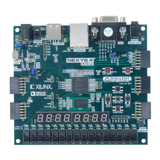
Nexys4 DDR™ FPGA Board Reference Manual
Nexys4 DDR rev. C; Revised April 11, 2016
1
Overview
The Nexys4 DDR board is a complete, ready-to-use digital circuit
development platform based on the latest Artix-7™ Field
Programmable Gate Array (FPGA) from Xilinx®. With its large,
high-capacity FPGA (Xilinx part number XC7A100T-1CSG324C),
generous external memories, and collection of USB, Ethernet, and
other ports, the Nexys4 DDR can host designs ranging from
introductory combinational circuits to powerful embedded
processors. Several built-in peripherals, including an
accelerometer, temperature sensor, MEMs digital microphone, a
speaker amplifier, and several I/O devices allow the Nexys4 DDR
to be used for a wide range of designs without needing any other
components.
The Artix-7 FPGA is optimized for high performance logic, and offers more capacity, higher performance, and more
resources than earlier designs. Artix-7 100T features include:
15,850 logic slices, each with four 6-input LUTs and 8 flip-flops
4,860 Kbits of fast block RAM
Six clock management tiles, each with phase-locked loop (PLL)
240 DSP slices
Internal clock speeds exceeding 450 MHz
On-chip analog-to-digital converter (XADC)
The Nexys4 DDR also offers an improved collection of ports and peripherals, including:
16 user switches
USB-UART Bridge
12-bit VGA output
3-axis accelerometer
128MiB DDR2
Pmod for XADC signals
The Nexys4 DDR is compatible with Xilinx's new high-performance Vivado® Design Suite as well as the ISE® toolset,
which includes ChipScope™ and EDK. Xilinx offers free WebPACK™ versions of these toolsets, so designs can be
implemented at no additional cost. The Nexys4 DDR is not supported by the Digilent Adept Utility.
DOC#: 502-292
16 user LEDs
Two tri-color LEDs
PWM audio output
Temperature sensor
Serial Flash
Digilent USB-JTAG port for FPGA
programming and
communication
Copyright Digilent, Inc. All rights reserved.
Other product and company names mentioned may be trademarks of their respective owners.
1300 Henley Court
Pullman, WA 99163
509.334.6306
www.digilentinc.com
The Nexys4 DDR
Two 4-digit 7-segment displays
Micro SD card connector
PDM microphone
10/100 Ethernet PHY
Four Pmod ports
USB HID Host for mice, keyboards
and memory sticks
Page 1 of 29
Advertisement
Table of Contents

Related Manuals for Digilent Nexys4 DDR


Summary of Contents for Digilent Nexys4 DDR
- Page 1 The Nexys4 DDR is compatible with Xilinx’s new high-performance Vivado® Design Suite as well as the ISE® toolset, which includes ChipScope™ and EDK. Xilinx offers free WebPACK™ versions of these toolsets, so designs can be implemented at no additional cost. The Nexys4 DDR is not supported by the Digilent Adept Utility.
- Page 2 Five pushbuttons Power switch Temperature sensor Power jack A growing collection of board support IP, reference designs, and add-on boards are available on the Digilent website. See the Nexys4 DDR page at www.digilentinc.com for more information. Copyright Digilent, Inc. All rights reserved.
-
Page 3: Power Supplies
Jumper JP3 (near the power jack) determines which source is used. All Nexys4 DDR power supplies can be turned on and off by a single logic-level power switch (SW16). A power-good LED (LD22), driven by the “power good” output of the ADP2118 supply, indicates that the supplies are turned on and operating normally. -
Page 4: Power Protection
An external battery pack can be used by connecting the battery’s positive terminal to the center pin of JP3 and the negative terminal to the pin labeled J12, directly below JP3. Since the main regulator on the Nexys4 DDR cannot accommodate input voltages over 5.5VDC, an external battery pack must be limited to 5.5VDC. -
Page 5: Jtag Configuration
Digilent USB-JTAG circuitry (port J6) or an external JTAG programmer, such as the Digilent JTAG-HS2, attached to port J10. You can perform JTAG programming any time after the Nexys4 DDR has been powered on, regardless of what the mode jumper (JP1) is set to. If the FPGA is already configured, then the existing configuration is overwritten with the bitstream being transmitted over JTAG. - Page 6 Bitstream compression, SPI bus width, and configuration rate are factors controlled by the Xilinx tools that can affect configuration speed. The Nexys4 DDR supports x1, x2, and x4 bus widths and data rates of up to 50 MHz for Quad-SPI programming.
- Page 7 USB keyboard is plugged in, a rapid blink will signal the receipt of an HID input report from the keyboard. Memory The Nexys4 DDR board contains two external memories: a 1Gib (128MiB) DDR2 SDRAM and a 128Mib (16MiB) non-volatile serial Flash device. The DDR2 modules are integrated on-board and connect to the FPGA using the industry standard interface.
-
Page 8: Ethernet Phy
The MIG Wizard will require the fixed pin-out of the memory signals to be entered and validated before generating the IP core. For your convenience, an importable UCF file is provided on the Digilent website to speed up the process. - Page 9 Oscillators/Clocks The Nexys4 DDR board includes a single 100 MHz crystal oscillator connected to pin E3 (E3 is a MRCC input on bank 35). The input clock can drive MMCMs or PLLs to generate clocks of various frequencies and with known phase relationships that may be needed throughout a design.
-
Page 10: Usb-Uart Bridge (Serial Port)
FT2232 within their design do not need to worry about the JTAG circuitry interfering with the UART data transfers, and vice-versa. The combination of these two features into a single device allows the Nexys4 DDR to be programmed, communicated with via UART, and powered from a computer attached with a single Micro USB cable. -
Page 11: Hid Controller
FPGA to create a keyboard or mouse interface. When a keyboard or mouse is connected to the Nexys4 DDR, a “self-test passed” command (0xAA) is sent to the host. After this, commands may be issued to the device. Since both the keyboard and the mouse use the same PS/2 port, one can tell the type of device connected using the device ID. - Page 12 Nexys4 DDR™ FPGA Board Reference Manual Keyboard PS/2-style keyboards use scan codes to communicate key press data. Each key is assigned a code that is sent whenever the key is pressed. If the key is held down, the scan code will be sent repeatedly about once every 100ms.
- Page 13 Nexys4 DDR™ FPGA Board Reference Manual Mouse Once entered in stream mode and data reporting is enabled, the mouse outputs a clock and data signal when it is moved; otherwise, these signals remain at logic ‘1.’ Each time the mouse is moved, three 11-bit words are sent from the mouse to the host device, as shown in Figure 10.
-
Page 14: Vga System Timing
VGA Port The Nexys4 DDR board uses 14 FPGA signals to create a VGA port with 4 bits-per-color and the two standard sync signals (HS – Horizontal Sync, and VS – Vertical Sync). The color signals use resistor-divider circuits that work in conjunction with the 75-ohm termination resistance of the VGA display to create 16 signal levels each on the red, green, and blue VGA signals. - Page 15 Nexys4 DDR™ FPGA Board Reference Manual Anode (entire screen) Cathode ray tube Deflection coils Electron guns Grid (Red, Blue, Green) Cathode ray R,G,B signals (to guns) cable High voltage supply deflection grid (>20kV) control control control Figure 12. Color CRT display.
- Page 16 (the pixel 479,0 pixel 479,639 Nexys4 DDR uses 12 bits per pixel). The controller must index into video memory Stable current ramp - information is as the beams move across the display, and displayed during this time...
- Page 17 Figure 15. VGA display controller block diagram. 10 Basic I/O The Nexys4 DDR board includes two tri-color LEDs, sixteen slide switches, six push buttons, sixteen individual LEDs, and an eight-digit seven-segment display, as shown in Figure 16. The pushbuttons and slide switches are connected to the FPGA via series resistors to prevent damage from inadvertent short circuits (a short circuit could occur if an FPGA pin assigned to a pushbutton or slide switch was inadvertently defined as an output).
- Page 18 Tri-Color LEDs 3.3V CPU Reset BTNRES Artix-7 Figure 16. General Purpose I/O devices on the Nexys4 DDR. Copyright Digilent, Inc. All rights reserved. Page 18 of 29 Other product and company names mentioned may be trademarks of their respective owners.
-
Page 19: Seven-Segment Display
To illuminate a segment, the anode should be driven high while the cathode is driven low. However, since the Nexys4 DDR uses transistors to drive enough current into the common anode point, the anode enables are inverted. Therefore, both the AN0..7 and the CA..G/DP signals are driven low when active. -
Page 20: Tri-Color Leds
10.2 Tri-Color LEDs The Nexys4 DDR board contains two tri-color LEDs. Each tri-color LED has three input signals that drive the cathodes of three smaller internal LEDs: one red, one blue, and one green. Driving the signal corresponding to one of these colors high will illuminate the internal LED. - Page 21 The Dual Analog/Digital Pmod on the Nexys4 DDR differs from the rest in the routing of its traces. The eight data signals are grouped into four pairs, with the pairs routed closely coupled for better analog noise immunity.
-
Page 22: Microsd Slot
Series FPGAs and Zynq-7000 All Programmable SoC XADC Dual 12-Bit 1 MSPS Analog-to-Digital Converter.” 12 MicroSD Slot The Nexys4 DDR provides a microSD slot for both FPGA configuration and user access. The on-board Auxiliary Function microcontroller shares the SD card bus with the FPGA. Before the FPGA is configured the microcontroller must have access to the SD card via SPI. -
Page 23: Open Drain Outputs
ADT7420 datasheet. 14 Accelerometer The Nexys4 DDR includes an Analog Device ADXL362 accelerometer. The ADXL362 is a 3-axis MEMS accelerometer that consumes less than 2μA at a 100Hz output data rate and 270nA when in motion triggered wake-up mode. -
Page 24: Spi Interface
15 Microphone The Nexys4 DDR board includes an omnidirectional MEMS microphone. The microphone uses an Analog Device ADMP421 chip which has a high signal to noise ratio (SNR) of 61dBA and high sensitivity of -26 dBFS. It also has a flat frequency response ranging from 100Hz to 15 kHz. - Page 25 Nexys4 DDR™ FPGA Board Reference Manual 15.1 Pulse Density Modulation (PDM) PDM data connections are becoming more and more popular in portable audio applications, such as cellphones and tablets. With PDM, two channels can be transmitted with only two wires. The frequency of a PDM signal usually falls in the range of 1 MHz to 3 MHz.
- Page 26 Nexys4 DDR™ FPGA Board Reference Manual 15.2 Microphone Digital Interface Timing The clock input of the microphone can range from 1 MHz to 3.3 MHz based on the sampling rate and data precision requirement of the applications. The L/R Select signal must be set to a valid level, depending on which edge of the clock the data bit will be read.
-
Page 27: Pulse-Width Modulation
Nexys4 DDR™ FPGA Board Reference Manual Figure 29. Sallen-Key Butterworth Low-Pass 4 Order Filter. The frequency response of SK Butterworth Low-Pass Filter is shown in Figure 30. The AC analysis of the circuit is done using NI Multisim 12.0. -100... -
Page 28: Built-In Self-Test
The source code and prebuilt bitstream for this design are available for download from the Digilent website. If the demo configuration is present in the flash and the Nexys4 DDR board is powered on in SPI mode, the demo project will allow basic hardware verification. Here is an overview of how this demo drives the different onboard components: ... - Page 29 Nexys4 DDR™ FPGA Board Reference Manual Stressed solder joints can be repaired by reheating and reflowing solder and contaminants can be cleaned with off- the-shelf electronics cleaning products. If a board fails test within the warranty period, it will be replaced at no cost.
- Page 30 Mouser Electronics Authorized Distributor Click to View Pricing, Inventory, Delivery & Lifecycle Information: Digilent 410-292P-KIT 410-292...
Need help?
Do you have a question about the Nexys4 DDR and is the answer not in the manual?
Questions and answers