Table of Contents
Advertisement
Advertisement
Chapters
Table of Contents

Related Manuals for Motorola MVME5500


Summary of Contents for Motorola MVME5500
- Page 1 MVME5500 Single-Board Computer Installation and Use V5500A/IH3 July 2005 Edition...
- Page 2 All rights reserved. Printed in the United States of America. Motorola and the stylized M logo are trademarks of Motorola, Inc., registered in the U.S. Patent and Trademark Office. All other product or service names mentioned in this document are the property of their...
- Page 3 The safety precautions listed below represent warnings of certain dangers of which Motorola is aware. You, as the user of the product, should follow these warnings and all other safety precautions necessary for the safe operation of the equipment in your operating environment.
- Page 4 Flammability All Motorola PWBs (printed wiring boards) are manufactured with a flammability rating of 94V-0 by UL-recognized manufacturers. EMI Caution This equipment generates, uses and can radiate electromagnetic energy. It Caution may cause or be susceptible to electromagnetic interference (EMI) if not installed and used with adequate EMI protection.
- Page 5 Warning Motorola Embedded Communications Computing products with the CE marking comply with the EMC Directive (89/336/EEC). Compliance with this directive implies conformity to the following European Norms: EN55022 “Limits and Methods of Measurement of Radio Interference Characteristics...
- Page 6 Electronic versions of this material may be read online, downloaded for personal use, or referenced in another document as a URL to the Motorola Web site. The text itself may not be published commercially in print or electronic form, edited, translated, or otherwise altered without the permission of Motorola, Inc.
-
Page 7: Table Of Contents
PCI Bus 1.0 Speed Header (J29) ..............1-15 EEPROM Write Protect Header (J30) ............1-16 Setting the PMC Vio Keying Pin ..............1-16 Hardware Installation ..................... 1-17 Installing the MVME5500 into a Chassis ............1-17 Connection to Peripherals ..................1-18 Completing the Installation ..................1-19... - Page 8 CHAPTER 2 Startup and Operation Introduction ......................2-1 Applying Power ......................2-1 Switches and Indicators .................... 2-1 CHAPTER 3 MOTLoad Firmware Introduction ......................3-1 Overview ......................3-1 MOTLoad Implementation and Memory Requirements ........3-1 MOTLoad Commands ..................3-2 MOTLoad Utility Applications ................. 3-2 MOTLoad Tests ....................
- Page 9 System Memory ....................... 4-7 PCI Local Buses and Devices .................. 4-8 Gigabit Ethernet Interface ................. 4-8 10/100Mb Ethernet Interface ................4-8 PCI-to-PCI Bridges ................... 4-9 PMC Sites ......................4-9 PCI IDSEL Definition ..................4-9 PCI Bus Arbitration ..................4-9 Asynchronous Serial Ports ..................4-10 Real Time Clock and NVRAM ................
- Page 10 Flash 0 Block Write Protect Header (J15) ............5-41 SROM Initialization Enable Header (J17) ............5-42 Bus Mode Select Header (J19) ................ 5-42 COP Enable Header (J20) ................5-43 PCI Bus 0.0 Speed Header (J25) ..............5-43 VME SCON Select Header (J27) ..............5-44 PCI Bus 1.0 Speed Header (J29) ..............
- Page 11 APPENDIX D Related Documentation Motorola Embedded Communications Computing Documents ......D-1 Manufacturers’ Documents ..................D-2 Related Specifications ....................D-5...
- Page 13 List of Figures Figure 1-1. MVME5500 Layout ................1-7 Figure 4-1. MVME5500 Block Diagram ..............4-3 Figure 4-2. COM1 Asynchronous Serial Port Connections (RJ-45) ..... 4-10 Figure 5-1. SBC/IPMC712 Mode ................. 5-37 Figure 5-2. SBC/IPMC761 Mode ................. 5-38 Figure 5-3. PMC Mode ..................5-39 Figure B-1.
- Page 15 List of Tables Table 1-1. Startup Overview ................... 1-2 Table 1-2. MVME5500 Jumper Settings ..............1-5 Table 1-3. MVME5500 Connectors ..............1-18 Table 2-1. Front-Panel LED Status Indicators ............2-2 Table 3-1. MOTLoad Commands ................3-7 Table 4-1. MVME5500 Features Summary ............4-1 Table 5-1.
- Page 16 Table 5-33. PCI Bus 1.0 Speed Header (J25) Pin Assignments ......5-44 Table 5-34. EEPROM Write Protect Header (J30) Pin Assignments ....5-45 Table A-1. Power Requirements ................A-1 Table A-2. MVME5500 Specifications ..............A-2 Table B-1. RAM5500 Feature Summary ..............B-1 Table B-2. RAM5500 Connector (P1) Pin Assignments ........B-5 Table C-1.
-
Page 17: Summary Of Changes
MVME5500 single-board computer. It provides specific preparation and installation information, and data applicable to the board. As of the printing date of this manual, the MVME5500 supports the models listed below. Model Number... -
Page 18: Overview Of Contents
Chapter 3, MOTLoad Firmware, describes the basic features of the MOTLoad firmware product. Chapter 4, Functional Description, describes the MVME5500 on a block diagram level. Chapter 5, Pin Assignments, provides pin assignments for various headers and connectors on the MMVE5500 single-board computer. -
Page 19: Comments And Suggestions
Comments and Suggestions Motorola welcomes and appreciates your comments on its documentation. We want to know what you think about our manuals and how we can make them better. Mail comments to: Motorola, Inc. Reader Comments DW278 2900 S. Diablo Way... - Page 20 <Enter>, <Return> or <CR> represents the carriage return or Enter key. Ctrl represents the Control key. Execute control characters by pressing the Ctrl key and the letter simultaneously, for example, Ctrl-d.
-
Page 21: Introduction
10/100 Ethernet port, 32MB expansion Flash ROM, two serial ports, NVRAM and a real-time clock. The MVME5500 interfaces to a VMEbus system via its P1 and P2 connectors and contains two IEEE 1386.1 PCI mezzanine card (PMC) slots. The PMC slots are 64-bit and support both front and rear I/O. -
Page 22: Getting Started
Hardware Preparation and Installation Getting Started This section provides an overview of the steps necessary to install and power up the MVME5500 and a brief section on unpacking and ESD precautions. Overview of Startup Procedures The following table lists the things you will need to do before you can use this board and tells where to find the information you need to perform each step. -
Page 23: Hardware Configuration
Avoid touching areas of integrated circuitry; static discharge can damage circuits. Caution Motorola strongly recommends that you use an antistatic wrist strap and a Use ESD conductive foam pad when installing or upgrading a system. Electronic components, such as disk drives, computer boards, and memory modules can be extremely sensitive to electrostatic discharge (ESD). -
Page 24: Mvme5500 Preparation
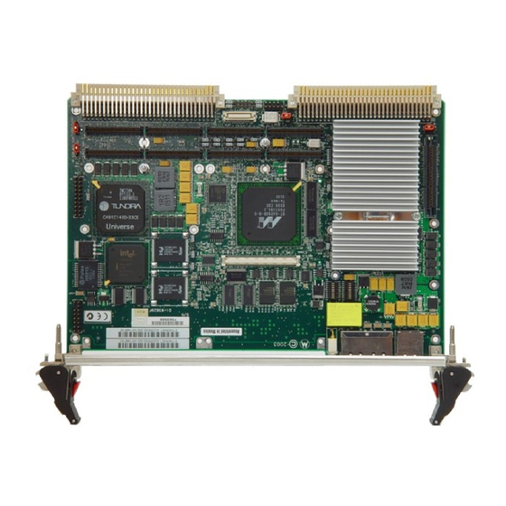
MVME5500 Preparation Figure 1-1 illustrates the placement of the jumpers, headers, connectors, and various other components on the MVME5500. There are several manually configurable headers on the MVME5500 and their settings are shown in Table 1-2. -
Page 25: Table 1-2. Mvme5500 Jumper Settings
MVME5500 Preparation For pin assignments on the MVME5500, refer to Chapter 5, Pin Assignments. Table 1-2. MVME5500 Jumper Settings Jumper Function Settings Ethernet 2 Selection 2-3 on all Rear P2 Ethernet (SBC mode) J100, Headers [1-2 on all] Front-panel Ethernet... - Page 26 Hardware Preparation and Installation Table 1-2. MVME5500 Jumper Settings (continued) Jumper Function Settings CPU COP Enable Header No jumper installed Enables boundary scan [1-2] Enables CPU COP PCI Bus 0.0 Speed Header [No jumper installed] PMC board controls whether the bus runs at 33 MHz or 66 MHz Forces PCI bus 0.0 to remain at...
-
Page 27: Figure 1-1. Mvme5500 Layout
MVME5500 Preparation Note Items in brackets are factory default settings. The MVME5500 is factory tested and shipped with the configuration described in the following section. J102 - J110 U129 J6 / J100 J101 / J7 U126 J15 J16 U123 U124 4202 0703 Figure 1-1. -
Page 28: Ethernet 2, Pmc/Sbc Mode, And P2 I/O Selection Headers (J6, J7, J28, J32, J34, J97 - J110)
For rear P2 Ethernet, install jumpers across pins 1-2 on all four headers when in SBC/IPMC761 mode. PMC/SBC Mode Selection The MVME5500 is set at the factory for SBC/IPMC712 mode. The SBC/IPMC761 mode should only be selected when using the IPMC761 module in conjunction with the MVME761 transition module.The PMC mode should be selected when using PMC modules with specific user I/O in conjunction with the corresponding transition module. -
Page 29: P2 I/O Selection
Nine 3-pin planar headers (J102 –J110) are for P2 I/O selection. Install jumpers across pins 1-2 on all nine headers when in PMC mode. Install jumpers across pins 2-3 on all nine headers when in SBC/IPMC761 or SBC/IPMC712 mode to connect the extended SCSI signals to P2. http://www.motorola.com/computer/literature... - Page 30 Hardware Preparation and Installation (factory configuration) Rear P2 Ethernet Front-Panel Ethernet 3 2 1 3 2 1 1 2 3 1 2 3 J100 J100 3 2 1 3 2 1 J101 J101 1 2 3 1 2 3 (factory configuration) PMC Mode SBC/IPMC761 Mode SBC/IPMC712 Mode...
-
Page 31: Flash Boot Bank Select Header (J8)
No jumper installed disables all Flash 0 programming. The jumper must be installed in order to erase array blocks, programming data, or configuring lock-bits. Disables Flash 0 writes Enables Flash 0 writes (factory configuration) http://www.motorola.com/computer/literature 1-11... -
Page 32: Safe Start Env Header (J10)
Hardware Preparation and Installation Safe Start ENV Header (J10) A 3-pin planar header selects programmed or safe start ENV settings. No jumper or a jumper across pins 1-2 indicates that the programmed ENV settings should be used during boot. A jumper across pins 2-3 indicates that the safe ENV settings should be used. -
Page 33: Srom Initialization Enable Header (J17)
A 3-pin planar header selects the processor bus operating mode. No jumper or a jumper across pins 1-2 selects the 60x bus mode while a jumper across pins 2-3 selects the MPX bus mode. 60x bus mode 60x bus mode MPX bus mode (factory configuration) http://www.motorola.com/computer/literature 1-13... -
Page 34: Cpu Cop Enable Header (J20)
Hardware Preparation and Installation CPU COP Enable Header (J20) A 2-pin planar header enables the Riscwatch capability. No jumper installed disables COP and enables boundary scan. A jumper across pins 1-2 enables the COP emulator debug. Disables COP; Enables COP enables boundary scan emulator debug (factory configuration) -
Page 35: Vme Scon Select Header (J27)
PCI 1.0 bus speed. A jumper installed across pins 1-2 forces PCI bus 1.0 to run at 33 MHz. PMC board controls Force PCI bus 1.0 PCI 1.0 bus speed to run at 33 MHz (factory configuration) http://www.motorola.com/computer/literature 1-15... -
Page 36: Eeprom Write Protect Header (J30)
Hardware Preparation and Installation EEPROM Write Protect Header (J30) A 2-pin planar header enables/disables programming of the on-board EEPROMs as a means of protecting the contents from being corrupted. No jumper installed disables EEPROM programming by driving the WP pin to a logic high. -
Page 37: Hardware Installation
2. Remove any filler panel that might fill that slot. 3. Install the top and bottom edge of the MVME5500 into the guides of the chassis. Only use injector handles for board insertion to avoid Warning damage/deformation to the front panel and/or PCB. -
Page 38: Connection To Peripherals
Hardware Preparation and Installation Connection to Peripherals When the MVME5500 is installed in a chassis, you are ready to connect peripherals and apply power to the board. Figure 1-1 on page 1-7 shows the locations of the various connectors while Table 1-3 lists them for you. -
Page 39: Completing The Installation
Verify that hardware is installed and the power/peripheral cables connected are appropriate for your system configuration. Replace the chassis or system cover, reconnect the system to the AC or DC power source, and turn the equipment power on. http://www.motorola.com/computer/literature 1-19... -
Page 41: Introduction
After you verify that all necessary hardware preparation is complete and all connections are made correctly, you can apply power to the system. When you are ready to apply power to the MVME5500: Verify that the chassis power supply voltage setting matches the voltage present in the country of use (if the power supply in your system is not auto-sensing). -
Page 42: Table 2-1. Front-Panel Led Status Indicators
Startup and Operation The MVME5500 has two front-panel indicators: BFL, software controlled. Asserted by firmware (or other software) to indicate a configuration problem (or other failure). CPU, connected to a CPU bus control signal to indicate bus activity. The following table describes these indicators: Table 2-1. -
Page 43: Introduction
The MVME5500 single-board computer (SBC) is offered with a wide range of memory (for example, DRAM, external cache, Flash). Typically, the smallest amount of on-board DRAM that a Motorola SBC has is 32MB. Each supported Motorola product line has its own unique... -
Page 44: Motload Commands
MOTLoad Firmware MOTLoad binary image(s). Currently the largest MOTLoad compressed image is less than 1MB in size. MOTLoad Commands MOTLoad supports two types of commands (applications): utilities and tests. Both types of commands are invoked from the MOTLoad command line in a similar fashion. Beyond that, MOTLoad utilities and MOTLoad tests are distinctly different. - Page 45 MOTLoad Firmware Package User’s Manual. Test results and test status are obtained through the testStatus, errorDisplay, and taskActive commands. Refer to the appropriate command description page in the MOTLoad Firmware Package User’s Manual for more information. http://www.motorola.com/computer/literature...
-
Page 46: Using Motload
MOTLoad then performs the specified action. An example of a MOTLoad command line prompt is shown below. The MOTLoad prompt changes according to what product it is used on (for example, MVME5500, MVME6100). Example: MVME5500>... -
Page 47: Command Line Help
MOTLoad RTOS Version 2.0 PAL Version 0.1 (Motorola MVME5500) Example: MVME5500> ver Copyright: Motorola Inc. 1999-2002, All Rights Reserved MOTLoad RTOS Version 2.0 PAL Version 0.1 (Motorola MVME5500) If the partial command string cannot be resolved to a single unique command, MOTLoad will inform the user that the command was ambiguous. -
Page 48: Command Line Rules
Option arguments immediately follow (no spaces) the option All commands, command options, device tree strings, etc., are case sensitive Example: MVME5500> flashProgram -d/dev/flash0 -n00100000 For more information on MOTLoad operation and function, refer to the MOTLoad Firmware Package User’s Manual. Literature Center Web Site... -
Page 49: Motload Command List
Block Verify Byte/Halfword/Word cdDir ISO9660 File System Directory Listing cdGet ISO9660 File System File Load clear Clear the Specified Status/History Table(s) Turns on Concurrent Mode devShow Display (Show) Device/Node Table diskBoot Disk Boot (Direct-Access Mass-Storage Device) http://www.motorola.com/computer/literature... - Page 50 MOTLoad Firmware Table 3-1. MOTLoad Commands (continued) Command Description downLoad Down Load S-Record from Host One-Line Instruction Disassembler echo Echo a Line of Text elfLoader ELF Object File Loader errorDisplay Display the Contents of the Test Error Status Table eval Evaluate Expression execProgram Execute Program...
- Page 51 Display PCI Device Configuration Header Register pciSpace Display PCI Device Address Space Allocation ping Ping Network Host portSet Port Set portShow Display Port Device Configuration Data User Program Register Display reset Reset System User Program Register Set Set Date and Time http://www.motorola.com/computer/literature...
- Page 52 MOTLoad Firmware Table 3-1. MOTLoad Commands (continued) Command Description sromRead SROM Read sromWrite SROM Write Symbol Table Attach Symbol Table Lookup stop Stop Date and Time (Power-Save Mode) taskActive Display the Contents of the Active Task Table Trace (Single-Step) User Program Trace (Single-Step) User Program to Address testDisk Test Disk...
- Page 53 Transparent Mode (Connect to Host) tsShow Display Task Status upLoad Up Load Binary-Data from Target version Display Version String(s) vmeCfg Manages user specified VME configuration parameters vpdDisplay VPD Display vpdEdit VPD Edit waitProbe Wait for I/O Probe to Complete http://www.motorola.com/computer/literature 3-11...
-
Page 54: Vme Settings
MOTLoad Firmware VME Settings As shipped from the factory, the firmware on the MVME5500 will program default values into the Universe II VME Interface chip. The firmware allows certain VME settings to be changed in order for the user to customize his/her environment. The following is a description of the default VME settings that are changeable by the user. - Page 55 VMEbus by this image is 0xB3FF0000. PCI Slave Image 3 Bound Address Register = B4000000 Sets LSI3_BD to indicate that the upper bound of PCI memory addresses to be transferred by this image is 0xB4000000. http://www.motorola.com/computer/literature 3-13...
- Page 56 MOTLoad Firmware PCI Slave Image 3 Translation Offset = 4C000000 Sets LSI3_TO to indicate that the PCI memory address is to be translated by 0x4C000000 before presentation on the VMEbus; the result of the translation is: 0xB3FF0000 + 0x4C000000 = 0xFFFF0000, thus 0xFFFF0000 on the VMEbus.
- Page 57 PCI addresses 0xB0000000 - 0xB1000000: VMEbus A24/D16 space, addresses 0xF0000000 - 0xF1000000. PCI addresses 0xB3FF0000 - 0xB4000000: VMEbus A16/D16 space, addresses 0xFFFF0000 - 0xFFFFFFFF. VMEbus A32/D32 addresses from 0x00000000 to (local DRAM size) address the local memory of the MVME5500. http://www.motorola.com/computer/literature 3-15...
-
Page 58: Cr/Csr Settings
MOTLoad Firmware The following sections provide additional information pertaining to the VME firmware settings of the MVME5500. A few VME settings are controlled by hardware jumpers while the majority of the VME settings are managed by the firmware command utility vmeCfg. -
Page 59: Editing Vme Settings
Edits Special PCI Target Image Register state vmeCfg -e -r400 Edits Master Control Register state vmeCfg -e -r404 Edits Miscellaneous Control Register state vmeCfg -e -r40C Edits User AM Codes Register state vmeCfg -e -rF70 Edits VMEbus Register Access Image Control Register state http://www.motorola.com/computer/literature 3-17... -
Page 60: Deleting Vme Settings
MOTLoad Firmware Deleting VME Settings To delete the changeable VME setting (restore default value), type the following at the firmware prompt: vmeCfg -d -m Deletes Master Enable state vmeCfg -d -i(0 - 7) Deletes selected Inbound Window state vmeCfg -d -o(0 - 7) Deletes selected Outbound Window state vmeCfg -d -r184 Deletes PCI Miscellaneous Register state... -
Page 61: Remote Start
Specification, listed in Appendix D, Related Documentation. The MVME5500 uses a Tundra Universe II for its VME bridge. The offsets of the mailboxes in the Universe II are defined in the Universe II User Manual, listed in Appendix D, Related... - Page 62 The MVME5500’s IBCA needs to be mapped appropriately through the master’s VMEbus bridge. For example, to use remote start using mailbox 0 on an MVME5500 installed in slot 5, the master would need a mapping to support reads and writes of address 0x002ff348 in VME CR/CSR space (0x280000 + 0x7f348).
-
Page 63: Features
4Functional Description This chapter describes the MVME5500 on a block diagram level. Features The following table lists the features of the MVME5500. Table 4-1. MVME5500 Features Summary Feature Description Processor – Single 1 GHz MPC7455 processor – Bus clock frequency at 133 MHz L3 Cache –... -
Page 64: Block Diagram
Functional Description Table 4-1. MVME5500 Features Summary (continued) Feature Description Interrupt Controller – Provided by GT-64260B – Interrupt sources internal to GT-64260B – Up to 32 external interrupt inputs – Up to seven interrupt outputs Counters/Timers – Eight 32-bit counters/timers in GT-64260B –... -
Page 65: Processor
L3 tag and controller, which supports a backside L3 cache. L3 Cache The MVME5500 uses two 8Mb DDR synchronous SRAM devices for the processor’s L3 cache data SRAM. This gives the processor a total of 2MB of L3 cache. These SRAM devices require a 2.5V core voltage. The... -
Page 66: System Controller
Functional Description MVME5500 provides 1.5V as the SRAM I/O voltage. The L3 bus operates at 200 MHz. System Controller The GT-64260B system controller for PowerPC architecture processors is a single chip solution that provides the following features: A 64-bit interface to the CPU bus A 64-bit SDRAM interface A 32-bit generic device interface for Flash, etc. -
Page 67: Memory Controller Interface
The GT-64260B can access up to four banks of SDRAM for a total of 1GB of SDRAM memory. The memory bus is capable of operating up to 133 MHz. The MVME5500 board has two banks on board and a connector for an expansion mezzanine board with two additional banks. Interrupt Controller... -
Page 68: Direct Memory Access (Dma)
In the second function, the controller is used by the system software to read the contents of the VPD EEPROM contained on the MVME5500 board, along with the SPD EEPROM(s), to further initialize the memory controller and other interfaces. -
Page 69: Flash Memory
MVME5500 product is built with the 128Mb devices. System Memory System memory for the MVME5500 is provided by one to four banks of ECC synchronous DRAM in two banks. During system initialization, the firmware determines the presence and configuration of each memory bank... -
Page 70: Pci Local Buses And Devices
Functional Description PCI Local Buses and Devices The GT-64260B on the MVME5500 provides two independent 64-bit, 33/66 MHz PCI buses. The GT-64260B documentation refers to these buses as PCI Bus 0 and PCI Bus 1. The devices on Bus 1 are the GT-64260B PCI bridge 1, one 32/64-bit PMC slot, and an 825544EI LAN device. -
Page 71: Pci-To-Pci Bridges
Computer Programmer’s Reference Guide. PCI Bus Arbitration PCI arbitration for the MVME5500 PCI Buses 0.0 and 1.0 is provided by an external arbiter PLD. The arbiter PLD implements a round-robin priority algorithm. PCI arbitration for PCI Bus 0.1 is provided by the HiNT PCI 6154 secondary internal arbiter. -
Page 72: Asynchronous Serial Ports
Figure 4-2. COM1 Asynchronous Serial Port Connections (RJ-45) Real Time Clock and NVRAM The SGS-Thomson M48T37V is used by the MVME5500 board to provide 32KB of non-volatile static RAM, real-time clock, and watchdog timer. The watchdog timer, if enabled, can be programmed to generate either an interrupt or system reset if it expires. -
Page 73: System Control And Status Registers
Registers mapped into Bank 1 of the GT-64260B device bus interface. Refer for the MMVE5500 Single-Board Computer Programmer’s Reference Guide for details. Sources of Reset The sources of reset on the MVME5500 are the following: Power-up Abort/Reset Switch NVRAM Watchdog Timer... -
Page 74: Pmc Expansion
Functional Description PMC Expansion The MVME5500 provides a PMC expansion connector to add more PMC interfaces than the two on the MVME5500 board. The connector is a Mictor AMP 767096-3 connector. Debug Support The MVME5500 provides a boundary scan header (J18) and a COP (Riscwatch) header for debug capability. -
Page 75: Introduction
5Pin Assignments Introduction This chapter provides pin assignments for various headers and connectors on the MMVE5500 single-board computer. Asynchronous Serial Port Connector (J1) on page 5-2 Ethernet Connectors (J2) on page 5-3 IPMC Connector (J3) on page 5-3 PCI/PMC Expansion Connector (J4) on page 5-5 CPU COP Connector (J5) on page 5-8 PMC 1 Interface Connectors (J11, J12, J13, J14) on page 5-8 Boundary Scan Connector (J18) on page 5-15... -
Page 76: Connectors
EEPROM Write Protect Header (J30) on page 5-45 Connectors Asynchronous Serial Port Connector (J1) An RJ-45 receptacle is located on the front panel of the MVME5500 board to provide the interface to the COM1 serial port. The pin assignments for this connector are as follows: Table 5-1. -
Page 77: Ethernet Connectors (J2)
Ethernet Connectors (J2) Ethernet Connectors (J2) Dual RJ-45 connectors are located on the front panel of the MVME5500 to provide the interface to the 10/100/1000BaseTX Ethernet ports. The pin assignments for these connectors are as follows: Table 5-2. Ethernet Connector (J2) Pin Assignments... - Page 78 Pin Assignments Table 5-3. IPMC Connector (J3) Pin Assignments Signal Signal DB10# +3.3V +3.3V DB11# DB12# DB13# DB14# +3.3V +3.3V DB15# DBP1# No Connect IPMC_INT +3.3V +3.3V REQ# GNT# +3.3V +5.0V +5.0V +5.0V +5.0V Computer Group Literature Center Web Site...
-
Page 79: Pci/Pmc Expansion Connector (J4)
Table 5-4. PCI/PMC Expansion Connector (J4) Pin Assignments Signal Signal +3.3V +3.3V PCICLK PMCINTA# PMCINTB# PURST# PMCINTC# HRESET# PMCINTD# TRST# PCIXP# PCIXGNT# PCIXREQ# +12V –12V PERR# SERR# LOCK# SDONE DEVSEL# SBO# TRDY# IRDY# STOP# FRAME# ACK64# Reserved REQ64# Reserved http://www.motorola.com/computer/literature... - Page 80 Pin Assignments Table 5-4. PCI/PMC Expansion Connector (J4) Pin Assignments (continued) Signal Signal PCIRST# C/BE1# C/BE0# C/BE3# C/BE2# AD11 AD10 AD13 AD12 AD15 AD14 AD17 AD16 AD19 AD18 AD21 AD20 AD23 AD22 AD25 AD24 AD27 AD26 AD29 AD28 AD31 AD30 Computer Group Literature Center Web Site...
- Page 81 Signal PAR64 Reserved C/BE5# C/BE4# C/BE7# C/BE6# AD33 AD32 AD35 AD34 AD37 AD36 AD39 AD38 AD41 AD40 AD43 AD42 AD45 AD44 AD47 AD46 AD49 AD48 AD51 AD50 AD53 AD52 AD55 AD54 AD57 AD56 AD59 AD58 AD61 AD60 AD63 AD62 http://www.motorola.com/computer/literature...
-
Page 82: Cpu Cop Connector (J5)
KEY (no pin) CHECKSTPO_L PMC 1 Interface Connectors (J11, J12, J13, J14) There are four 64-pin SMT connectors for the PMC 1 slot on the MVME5500 to provide a 32/64-bit PCI interface and optional I/O interface. Computer Group Literature Center Web Site... -
Page 83: Table 5-6. Pmc 1 Connector (J11) Pin Assignments
Table 5-6. PMC 1 Connector (J11) Pin Assignments Signal Signal –12V INTA# INTB# INTC# PRESENT# INTD# PCI_RSVD +3.3Vaux GNT#/XREQ0# REQ#/XGNT0# AD31 AD28 AD27 AD25 C/BE3# AD22 AD21 AD19 AD17 FRAME# IRDY# DEVSEL# LOCK# PCI_RSVD PCI_RSVD http://www.motorola.com/computer/literature... -
Page 84: Table 5-7. Pmc 1 Connector (J12) Pin Assignments
Pin Assignments Table 5-6. PMC 1 Connector (J11) Pin Assignments Signal Signal AD15 AD12 AD11 AD09 C/BE0# AD06 AD05 AD04 AD03 AD02 AD01 AD00 REQ64# Table 5-7. PMC 1 Connector (J12) Pin Assignments Signal Signal +12V TRST# PCI_RSVD PCI_RSVD PCI_RSVD MOT_RSVD +3.3V RST#... - Page 85 Table 5-7. PMC 1 Connector (J12) Pin Assignments Signal Signal IDSEL AD23 +3.3V AD20 AD18 AD16 C/BE2# IDSELB TRDY# +3.3V STOP# PERR# +3.3V SERR# C/BE1# AD14 AD13 M66EN AD10 AD08 +3.3V AD07 REQB_L +3.3V GNTB_L MOT_RSVD MOT_RSVD EREADY NC (RESETOUT_L) 60 ACK64# +3.3V NC (MONARCH#) http://www.motorola.com/computer/literature 5-11...
-
Page 86: Table 5-8. Pmc 1 Connector (J13) Pin Assignments
Pin Assignments Table 5-8. PMC 1 Connector (J13) Pin Assignments Signal Signal PCI_RSVD C/BE7# C/BE6# C/BE5# C/BE4# PAR64 AD63 AD62 AD61 AD60 AD59 AD58 AD57 AD56 AD55 AD54 AD53 AD52 AD51 AD50 AD49 AD48 AD47 AD46 AD45 AD44 AD43 AD42 AD41 AD40 AD39... -
Page 87: Table 5-9. Pmc 1 Connector (J14) Pin Assignments
PMC1_12 (P2-A6) PMC1_13 (P2-C7) PMC1_14 (P2-A7) PMC1_15 (P2-C8) PMC1_16 (P2-A8) PMC1_17 (P2-C9) PMC1_18 (P2-A9) PMC1_19 (P2-C10) PMC1_20 (P2-A10) PMC1_21 (P2-C11) PMC1_22 (P2-A11) PMC1_23 (P2-C12) PMC1_24 (P2-A12) PMC1_25 (P2-C13) PMC1_26 (P2-A13) PMC1_27 (P2-C14) PMC1_28 (P2-A14) PMC1_29 (P2-C15) PMC1_30 (P2-A15) http://www.motorola.com/computer/literature 5-13... - Page 88 Pin Assignments Table 5-9. PMC 1 Connector (J14) Pin Assignments Signal Signal PMC1_31 (P2-C16) PMC1_32 (P2-A16) PMC1_33 (P2-C17) PMC1_34 (P2-A17) PMC1_35 (P2-C18) PMC1_36 (P2-A18) PMC1_37 (P2-C19) PMC1_38 (P2-A19) PMC1_39 (P2-C20) PMC1_40 (P2-A20) PMC1_41 (P2-C21) PMC1_42 (P2-A21) PMC1_43 (P2-C22) PMC1_44 (P2-A22) PMC1_45 (P2-C23) PMC1_46 (P2-A23) PMC1_47 (P2-C24)
-
Page 89: Boundary Scan Connector (J18)
Boundary Scan Connector (J18) Boundary Scan Connector (J18) The boundary scan connector is used to provide boundary scan testing of all on-board JTAG devices in a single scan chain. Table 5-10. Boundary Scan Connector (J18) Pin Assignments Signal Signal TRST_L http://www.motorola.com/computer/literature 5-15... -
Page 90: Pmc 2 Interface Connectors (J21, J22, J23, J24)
PMC 2 Interface Connectors (J21, J22, J23, J24) There are four 64-pin SMT connectors for the PMC 2 slot on the MVME5500 to provide a 32/64-bit PCI interface and optional I/O interface. Table 5-11. PMC 2 Connector (J21) Pin Assignments... -
Page 91: Table 5-12. Pmc 2 Connector (J22) Pin Assignments
AD15 AD12 AD11 AD09 C/BE0# AD06 AD05 AD04 AD03 AD02 AD01 AD00 REQ64# Table 5-12. PMC 2 Connector (J22) Pin Assignments Signal Signal +12V TRST# PCI_RSVD PCI_RSVD PCI_RSVD MOT_RSVD +3.3V RST# MOT_RSVD +3.3V MOT_RSVD PME# AD30 AD29 AD26 http://www.motorola.com/computer/literature 5-17... - Page 92 Pin Assignments Table 5-12. PMC 2 Connector (J22) Pin Assignments Signal Signal AD24 +3.3V IDSEL AD23 +3.3V AD20 AD18 AD16 C/BE2# IDSELB TRDY# +3.3V STOP# PERR# +3.3V SERR# C/BE1# AD14 AD13 M66EN AD10 AD08 +3.3V AD07 REQB_L +3.3V GNTB_L MOT_RSVD MOT_RSVD EREADY NC (RESETOUT_L)
-
Page 93: Table 5-13. Pmc 2 Connector (J23) Pin Assignments
Table 5-13. PMC 2 Connector (J23) Pin Assignments Signal Signal PCI_RSVD C/BE7# C/BE6# C/BE5# C/BE4# PAR64 AD63 AD62 AD61 AD60 AD59 AD58 AD57 AD56 AD55 AD54 AD53 AD52 AD51 AD50 AD49 AD48 AD47 AD46 AD45 AD44 AD43 AD42 AD41 AD40 AD39 AD38 AD37 http://www.motorola.com/computer/literature 5-19... -
Page 94: Table 5-14. Pmc 2 Connector (J24) Pin Assignments
Pin Assignments Table 5-13. PMC 2 Connector (J23) Pin Assignments Signal Signal AD36 AD35 AD34 AD33 AD32 PCI_RSVD PCI_RSVD PCI_RSVD PCI_RSVD Table 5-14. PMC 2 Connector (J24) Pin Assignments Signal Signal PMC2_1 (P2-D1) PMC2_2 (P2-Z1) PMC2_3 (P2-D2) PMC2_4 (P2-D3) PMC2_5 (P2-Z3) PMC2_6 (P2-D4) PMC2_7 (P2-D5) PMC2_8 (P2-Z5) - Page 95 PMC2_46 (P2-Z31) Not Used Not Used Not Used Not Used Not Used Not Used Not Used Not Used Not Used Not Used Not Used Not Used Not Used Not Used Not Used Not Used Not Used Not Used http://www.motorola.com/computer/literature 5-21...
-
Page 96: Asynchronous Serial Port (Com2) Planar Connector (J33)
Documentation, for the link to this specification). Row B of the P2 connector provides power to the MVME5500 and to the upper eight VMEbus address lines, and additional 16 VMEbus data lines. The pin assignments for the P2 connector are as follows: Warning When J28 is configured for IPMC mode, –12V is supplied to P2 pin A30. -
Page 97: Table 5-16. Vme Connector (P2) Pin Assignments (Pmc Mode)
PMC1_18 VA29 PMC1_17 (J14-17) PMC2_13 (J24-13) (J24-14) (J14-18) PMC1_20 VA30 PMC1_19 (J14-19) PMC2_15 (J24-15) (J14-20) PMC2_17 PMC1_22 VA31 PMC1_21 (J14-21) PMC2_16 (J24-16) (J24-17) (J14-22) PMC1_24 PMC1_23 (J14-23) PMC2_18 (J24-18) (J14-24) PMC2_20 PMC1_26 PMC1_25 (J14-25) PMC2_19 (J24-19) (J24-20) (J14-26) http://www.motorola.com/computer/literature 5-23... - Page 98 Pin Assignments Table 5-16. VME Connector (P2) Pin Assignments (PMC Mode) ROW Z ROW A ROW B ROW C ROW D PMC1_28 VD16 PMC1_27 (J14-27) PMC2_21 (J24-21) (J14-28) PMC2_23 PMC1_30 VD17 PMC1_29 (J14-29) PMC2_22 (J24-22) (J24-23) (J14-30) PMC1_32 VD18 PMC1_31 (J14-31) PMC2_24 (J24-24) (J14-32) PMC2_26...
-
Page 99: Vmebus Connectors (P1 & P2) (Sbc Mode)
Documentation, for the link to this specification). Row B of the P2 connector provides power to the MVME5500 and to the upper eight VMEbus address lines, and additional 16 VMEbus data lines. The pin assignments for the P2 connector are as follows: Warning When J28 is configured for IPMC mode, –12V is supplied to P2 pin A30. -
Page 100: Table 5-17. Vme Connector (P2) Pinout With Ipmc712
Pin Assignments J102 – J110 should be configured for IPMC I/O to connect the IPMC extended SCSI signals from J3 to the P2 connector. Table 5-17. VME Connector (P2) Pinout with IPMC712 Row Z Row A Row B Row C Row D PMC2_2 DB0#... -
Page 101: Table 5-18. Vme Connector (P2) Pinouts With Ipmc761
DB5# VA26 Not Used PMC2_9 (J24-9) DB11# DB6# VA27 +12VF PMC2_10 (J24-10) DB7# VA28 PRSTB# PMC2_12 (J24-12) DB12# DBP# VA29 PRD0 PMC2_13 (J24-13) ATN# VA30 PRD1 PMC2_15 (J24-15) DB13# BSY# VA31 PRD2 PMC2_16 (J24-16) ACK# PRD3 PMC2_18 (J24-18) http://www.motorola.com/computer/literature 5-27... - Page 102 Pin Assignments Table 5-18. VME Connector (P2) Pinouts with IPMC761 (continued) Row Z Row A Row B Row C Row D DB14# RST# PRD4 PMC2_19 (J24-19) MSG# VD16 PRD5 PMC2_21 (J24-21) DB15# SEL# VD17 PRD6 PMC2_22 (J24-22) D/C# VD18 PRD7 PMC2_24 (J24-24) DBP1# REQ#...
-
Page 103: Memory Expansion Connector (P4)
Rows A and C and Z’s (Z1, 3, 5, 7, 9, 11, 13, 15, and 17) functionality is provided by the IPMC761 in slot 1 and the MVME5500 Ethernet port 2. Memory Expansion Connector (P4) One 140-pin connector is used to provide memory expansion capability. - Page 104 Pin Assignments Table 5-19. Memory Expansion Connector (P4) Pin Assignments (continued) Signal Signal MD22 MD23 +3.3V +3.3V MD24 MD25 MD26 MD27 MD28 MD29 MD30 MD31 MD32 MD33 MD34 MD35 MD36 MD37 MD38 MD39 +3.3V +3.3V MD40 MD41 MD42 MD43 MD44 MD45 MD46 MD47...
- Page 105 Assignments (continued) Signal Signal MD62 MD63 MPAR0 MPAR1 MPAR2 MPAR3 MPAR4 MPAR5 +3.3V +3.3V MPAR6 MPAR7 BA0# BA1# MA12 MA11 MA10 +3.3V +3.3V B2_CS# B3_CS# DQM5 DQM7 SDWE# SDRAS# SDCAS# +3.3V +3.3V DQM6 DQM5 I2CSCL I2CSDA A1_SPD (GND) 128 http://www.motorola.com/computer/literature 5-31...
- Page 106 Pin Assignments Table 5-19. Memory Expansion Connector (P4) Pin Assignments (continued) Signal Signal A0_SPD (NC) DQM4 DQM3 DQM2 CLK_MEZZ +3.3V DQM1 DQM0 5-32 Computer Group Literature Center Web Site...
-
Page 107: Headers
P2_TX+ J100 J101 FP_RX+ FP_TX– TX– P2_RX+ P2_TX– For rear P2 Ethernet, install jumpers across pins 2-3 on all four headers (J6, J7, J100, and J101). For front-panel Ethernet, install jumpers across pins 1-2 on all four headers. http://www.motorola.com/computer/literature 5-33... -
Page 108: Pmc/Sbc Mode Selection
J99) when in SBC/IPMC761 mode. No jumpers are installed for front- panel Ethernet. PMC/SBC Mode Selection Two 3-pin planar headers on the MVME5500 are for PMC/SBC mode selection. For PMC mode, install jumpers across pins 1-2 on both headers. For SBC/IPMC761 mode, install jumpers across pins 2-3 on both headers. -
Page 109: P2 I/O Selection
Nine 3-pin 2 mm planar headers are for P2 I/O selection. Install jumpers across pins 1-2 on all nine headers to select PMC 2 I/O for P2 in PMC mode. Install jumpers across pins 2-3 on all nine headers to select IPMC http://www.motorola.com/computer/literature 5-35... -
Page 110: Table 5-23. P2 I/O Selection Headers (J102 - J110) Pin Assignments
Pin Assignments I/O for P2 in SBC/IPMC761 or SBC/IPMC712 mode. The pin assignments for these headers are as follows: Table 5-23. P2 I/O Selection Headers (J102 – J110) Pin Assignments Signal Signal J102 J103 PMC2_IO (2) PMC2_IO (5) P2_PMC2_IO (2) P2_PMC2_IO (5) IPMC_DB8_L IPMC_DB9_L... -
Page 111: Figure 5-1. Sbc/Ipmc712 Mode
Ethernet 2, PMC/SBC Mode, and P2 I/O Selection Headers (J6, J7, J28, J32, J34, J97 – J110) Figure 5-1. SBC/IPMC712 Mode http://www.motorola.com/computer/literature 5-37... -
Page 112: Figure 5-2. Sbc/Ipmc761 Mode
Pin Assignments Figure 5-2. SBC/IPMC761 Mode 5-38 Computer Group Literature Center Web Site... -
Page 113: Figure 5-3. Pmc Mode
Ethernet 2, PMC/SBC Mode, and P2 I/O Selection Headers (J6, J7, J28, J32, J34, J97 – J110) Figure 5-3. PMC Mode http://www.motorola.com/computer/literature 5-39... -
Page 114: Flash Boot Bank Select Header (J8)
Pin Assignments Flash Boot Bank Select Header (J8) A 3-pin 2 mm planar header selects the boot Flash bank. No jumper or a jumper installed across pins 1-2 selects Flash 0 as the boot bank. A jumper installed across pins 2-3 selects Flash 1 as the boot bank. The pin assignments for this header are as follows: Table 5-24. -
Page 115: Safe Start Env Header (J10)
Refer to the Intel K3 Flash data sheet for further details. The pin assignments for this header are as follows: Table 5-27. Flash 0 Write Protect Header (J15) Pin Assignments Signal +3.3V WP_L http://www.motorola.com/computer/literature 5-41... -
Page 116: Srom Initialization Enable Header (J17)
Pin Assignments SROM Initialization Enable Header (J17) A 3-pin 2 mm planar header enables/disables the GT-64260B SROM initialization. No jumper or a jumper across pins 1-2 enables the GT-64260B device initialization via I2C SROM while a jumper across pins 2-3 disables this initialization sequence. The pin assignments for this header are as follows: Table 5-28. -
Page 117: Cop Enable Header (J20)
0.0 speed. A jumper installed across pins 1-2 forces PCI Bus 0.0 to run at 33 MHz. The pin assignments for this header are as follows: Table 5-31. PCI Bus 0.0 Speed Header (J25) Pin Assignments Signal P0_M66EN http://www.motorola.com/computer/literature 5-43... -
Page 118: Vme Scon Select Header (J27)
Pin Assignments VME SCON Select Header (J27) A 3-pin 2 mm planar header allows the choice for auto/enable/disable SCON VME configuration. A jumper installed across pins 1-2 configures for SCON disabled. A jumper installed across pins 2-3 configures for auto SCON. -
Page 119: Eeprom Write Protect Header (J30)
WP pin to a logic high. The jumper must be installed in order to program any of the EEPROMs at addresses A0, A6, A8, and/or AA. The pin assignments for this header are as follows: Table 5-34. EEPROM Write Protect Header (J30) Pin Assignments Signal I2CWP http://www.motorola.com/computer/literature 5-45... -
Page 121: Power Requirements
ASpecifications Power Requirements In its standard configuration, the MVME5500 requires +5V, +12V, and –12V for operation. On-board converters supply the processor core voltage, +3.3V, +1.5V, +1.8V, and +2.5V. Supply Current Requirements Table A-1 provides an estimate of the typical and maximum current required from each of the input supply voltages. -
Page 122: Environmental Specifications
Specifications Environmental Specifications Table A-2 lists the environmental specifications, along with the board dimensions. Table A-2. MVME5500 Specifications Characteristics Specifications Operating Temperature 0° to +55° C (forced air cooling required) 400 LFM (linear feet per minute) of forced air cooling is recommended for operation in the upper temperature range. -
Page 123: Appendix B Ram5500 Memory Expansion Module
The following sections describe the physical and electrical structure of the RAM5500 memory expansion module. RAM5500 Description The RAM5500 is a memory expansion module that is used on the MVME5500 single board computer. It is based on a single memory... -
Page 124: Figure B-1. Ram5500 Block Diagram
ECC memory using 256Mb devices in 32MB x 8 device organization. The RAM5500 provides a total added capacity of 512MB to the MVME5500. The SDRAM memory is controlled by the GT-64260B, which provides single-bit error correction and double-bit error detection. -
Page 125: Clocks
VME boards. 3. Carefully remove the MVME5500 from its VME card slot and lay it flat, with connectors P1 and P2 facing you. 4. Inspect the RAM5500 module that is being installed on the MVME5500 host board to ensure that standoffs are installed in the four mounting holes on the module. - Page 126 RAM5500 Memory Expansion Module the four holes and the P4 connector on the MVME5500 host board and press the two connectors together until they are firmly seated in place. 4237 0903 6. Turn the entire assembly over and fasten the four short Phillips screws to the standoffs of the RAM5500.
-
Page 127: Memory Expansion Connector (P1) Pin Assignments
Table B-2. RAM5500 Connector (P1) Pin Assignments GND* GND* DQ00 DQ01 DQ02 DQ03 DQ04 DQ05 DQ06 DQ07 +3.3V +3.3V DQ08 DQ09 DQ10 DQ11 DQ12 DQ13 DQ14 DQ15 GND* GND* DQ16 DQ17 DQ18 DQ19 DQ20 DQ21 DQ22 DQ23 +3.3V +3.3V DQ24 DQ25 DQ26 DQ27 DQ28 DQ29 http://www.motorola.com/computer/literature... - Page 128 RAM5500 Memory Expansion Module Table B-2. RAM5500 Connector (P1) Pin Assignments DQ30 DQ31 GND* GND* DQ32 DQ33 DQ34 DQ35 DQ36 DQ37 DQ38 DQ39 +3.3V +3.3V DQ40 DQ41 DQ42 DQ43 DQ44 DQ45 DQ46 DQ47 GND* GND* DQ48 DQ49 DQ50 DQ51 DQ52 DQ53 +3.3V +3.3V...
- Page 129 Memory Expansion Connector (P1) Pin Assignments Table B-2. RAM5500 Connector (P1) Pin Assignments CKD06 CKD07 GND* GND* +3.3V +3.3V CS_C_L CS_D_L GND* DQM8 DQM7 WE_L RAS_L GND* GND* CAS_L +3.3V +3.3V DQM6 DQM5 A1_SPD A0_SPD DQM4 DQM3 DQM2 SDRAMCLK1 +3.3V DQM1 DQM0 GND* GND* http://www.motorola.com/computer/literature...
-
Page 130: Ram5500 Programming Issues
This register is partially described for the RAM5500 within the MVME5500 Single Board Computer Programmer’s Reference Guide. The register is accessed through the I2C interface of the GT-64260B on the host board (MVME5500). The RAM5500 SPD is software addressable by a unique address. Literature Center Web Site... -
Page 131: Thermally Significant Components
These operating conditions vary depending on system design. While Motorola performs thermal analysis in a representative system to verify operation within specified ranges, refer to Appendix A, Specifications, you should evaluate the thermal performance of the board in your application. -
Page 132: Table C-1. Thermally Significant Components
Thermal Validation refers to the temperature at the top, center surface of the component. Air temperature refers to the ambient temperature near the component. Table C-1. Thermally Significant Components Max. Allowable Component Reference Temperature Measurement Designator Generic Description (deg. C) Location U2, U3 Flash, soldered... -
Page 133: Figure C-1. Thermally Significant Components-Primary Side
Thermally Significant Components J102 - J110 U129 J6 / J100 J101 / J7 U126 J15 J16 U123 U124 4202 0703 Figure C-1. Thermally Significant Components—Primary Side http://www.motorola.com/computer/literature... -
Page 134: Figure C-2. Thermally Significant Components-Secondary Side
Thermal Validation U100 4203 0203 Figure C-2. Thermally Significant Components—Secondary Side Literature Center Web Site... -
Page 135: Component Temperature Measurement
Make sure that the thermocouple junction contacts only the electrical component. Also make sure that heatsinks lay flat on electrical components. The following figure shows one method of machining a heatsink base to provide a thermocouple routing path. http://www.motorola.com/computer/literature... - Page 136 Thermal Validation Note Machining a heatsink base reduces the contact area between the heatsink and the electrical component. You can partially compensate for this effect by filling the machined areas with thermal grease. The grease should not contact the thermocouple junction.
-
Page 137: Figure C-3. Mounting A Thermocouple Under A Heatsink
Machined groove for Through hole for thermocouple thermocouple wire junction clearance (may require routing removal of fin material) Also use for alignment guidance during heatsink installation Thermal pad Heatsink base HEATSINK BOTTOM VIEW Figure C-3. Mounting a Thermocouple Under a Heatsink http://www.motorola.com/computer/literature... -
Page 138: Measuring Local Air Temperature
Thermal Validation Measuring Local Air Temperature Measure local component ambient temperature by placing the thermocouple downstream of the component. This method is conservative since it includes heating of the air by the component. The following figure illustrates one method of mounting the thermocouple. Tape thermocouple wire to top of component Thermocouple... -
Page 139: Table D-1. Motorola Ecc Documents
DRelated Documentation Motorola Computer Group Documents The Motorola publications listed below are referenced in this manual. You can obtain electronic copies of Motorola Embedded Communications Computing (ECC) publications by: Contacting your local Motorola sales office Visiting Motorola ECC’s World Wide Web literature site, http://www.motorola.com/computer/literature... -
Page 140: Table D-2. Manufacturers' Documents
Table D-2. Manufacturers’ Documents Document Title and Source Publication Number MPC7450 RISC Microprocessor User’s Manual MPC7450UM/D Rev 2 Literature Distribution Center for Motorola Telephone: 1-800- 441-2447 FAX: (602) 994-6430 or (303) 675-2150 Web Site: http://e- www.motorola.com/webapp/sps/library/prod_lib.jsp E-mail: ldcformotorola@hibbertco.com... - Page 141 3 Volt Intel StrataFlash Memory 290667-005 28F128J3A, 28F640J3A, 28F320J3A Intel Corporation Literature Center 19521 E. 32nd Parkway Aurora CO 80011-8141 Web Site: http://www.intel.com/design/litcentr/index.htm PCI 6154 (HB2) PCI-to-PCI Bridge Data Book 6154_DataBook_v2.0.p PLX Technology, Inc. 870 Maude Avenue Sunnyvale, California 94085 Web Site: http://www.hintcorp.com/products/hint/default.asp http://www.motorola.com/computer/literature...
- Page 142 Related Documentation Table D-2. Manufacturers’ Documents (continued) Document Title and Source Publication Number TL16C550C Universal Asynchronous Receiver/Transmitter SLLS177E Texas Instruments P. O. Box 655303 Dallas, Texas 75265 Web Site: http://www.ti.com 3.3V-5V 256Kbit (32Kx8) Timekeeper SRAM M48T37V ST Microelectronics 1000 East Bell Road Phoenix, AZ 85022 Web Site: http://eu.st.com/stonline/index.shtml...
-
Page 143: Table D-3. Related Specifications
Revision 2.0, 2.1, 2.2 Specification IEEE http://standards.ieee.org/catalog/ IEEE - Common Mezzanine Card Specification (CMC) Institute of P1386 Draft 2.0 Electrical and Electronics Engineers, Inc. IEEE - PCI Mezzanine Card Specification (PMC) P1386.1 Draft 2.0 Institute of Electrical and Electronics Engineers, Inc. http://www.motorola.com/computer/literature... - Page 145 Index Numerics delete 3-18 display 3-16 10/100Mb Ethernet edit 3-17 restore 3-18 abort/reset switch delete VME settings 3-18 air temperature range dimensions ambient temperature, measuring display VME settings 3-16 ambient temperatures documentation, related applying power asynchronous serial ports 4-10 edit VME settings 3-17 environmental specifications block diagram...
- Page 146 MOTLoad prompt explained humidity test suites tests described indicators MPC7455 processor install MVME5500 1-17 NVRAM 4-10 RAM5500 installation, completing 1-19 operating temperatures, maximum jumper settings 1-5, 1-16 P1 connector PCI bus arbitration...
- Page 147 Vio keying pin 1-16 I2C serial interface/devices VME settings 3-12 interrupt controller delete 3-18 memory controller interface 4-5, display 3-16 timers edit 3-17 system memory restore 3-18 vmeCfg 3-16 temperature measurement C-1, temperature range temperatures, component watchdog timer 4-10 http://www.motorola.com/computer/literature IN-3...
Need help?
Do you have a question about the MVME5500 and is the answer not in the manual?
Questions and answers