Table of Contents
Advertisement
Quick Links
Advertisement
Table of Contents

Related Manuals for Motorola MVME2301


Summary of Contents for Motorola MVME2301
- Page 1 MVME2300-Series VME Processor Module Installation and Use V2300A/IH2...
- Page 2 Motorola, Inc. assumes no liability resulting from any omissions in this document, or from the use of the information obtained therein. Motorola reserves the right to revise this document and to make changes from time to time in the content hereof without obligation of Motorola to notify any person of such revision or changes.
- Page 3 MPC603 or MPC604 PowerPC microprocessor, and features dual PCI Mezzanine Card (PMC) slots with front panel and/or P2 I/O. The MVME2300 is currently available in the following conÞgurations: Model Memory MVME2301 MPC603 16MB ECC DRAM @ 200 MHz MVME2302 32MB ECC DRAM...
- Page 4 This manual is intended for anyone who wants to design OEM systems, supply additional capability to an existing compatible system, or work in a lab environment for experimental purposes. A basic knowledge of computers and digital logic is assumed. Document Terminology Throughout this manual, a convention is used which precedes data and address parameters by a character identifying the numeric format as follows: Dollar...
- Page 5 Motorola, Inc. assumes no liability for the customer's failure to comply with these requirements. The safety precautions listed below represent warnings of certain dangers of which Motorola is aware. You, as the user of the product, should follow these warnings and all other safety precautions necessary for the safe operation of the equipment in your operating environment.
- Page 6 ßammability rating of 94V-0. The computer programs stored in the Read Only Memory of this device contain material copyrighted by Motorola Inc., 1995, and may be used only under a license such as those contained in MotorolaÕs software licenses.
- Page 7 ¨ Motorola and the Motorola symbol are registered trademarks of Motorola, Inc. PowerPCª is a trademark of International Business Machines Corporation and is used by Motorola with permission. All other products mentioned in this document are trademarks or registered trademarks of their respective holders.
-
Page 9: Table Of Contents
Contents Chapter 1 Preparing and Installing the MVME2300-Series Module Introduction ......................1-1 MVME230x Description ..................1-1 MVME230x Module ..................1-2 PMCspan Expansion Mezzanine..............1-3 PCI Mezzanine Cards (PMCs) ..............1-3 VMEsystem Enclosure ..................1-4 System Console Terminal ................1-4 Overview of Start-Up Procedures..............1-4 Unpacking the MVME230x Hardware..............1-7 Preparing the MVME230x Hardware..............1-7 MVME230x .....................1-7... - Page 10 RST (S2) ....................2-3 Status Indicators .................... 2-4 BFL (DS1) ....................2-4 CPU (DS2) ....................2-4 PMC (DS3) ....................2-4 PMC (DS4) ....................2-4 10/100 BASET Port ..................2-4 DEBUG Port ....................2-5 PMC Slots ....................... 2-6 PCI MEZZANINE CARD (PMC Slot 1) ..........2-6 PCI MEZZANINE CARD (PMC Slot 2) ..........
- Page 11 ......................5-5 Debugger Commands ...................5-6 Diagnostic Tests....................5-10 Chapter 6 Modifying the Environment Overview .......................6-1 CNFG - ConÞgure Board Information Block ...........6-2 ENV - Set Environment ..................6-3 ConÞguring the PPCBug Parameters ............6-3 ConÞguring the VMEbus Interface ............6-13 Motorola Computer Group Documents ............A-1...
- Page 12 ManufacturersÕ Documents ................A-2 Related SpeciÞcations..................A-5 SpeciÞcations ......................B-1 Cooling Requirements..................B-3 EMC Regulatory Compliance ................B-4 Introduction ......................C-1 Assignments....................C-1 VMEbus Connector - P1 ................C-2 VMEbus Connector - P2 ................C-4 Serial Port Connector - DEBUG (J2)............C-6 Ethernet Connector - 10BASET (J3) ............
- Page 13 Figures Figure 1-1. MVME230x Switches, LEDs, Headers, Connectors....1-9 Figure 1-2. General-Purpose Software-Readable Header......1-12 Figure 1-3. Typical Single-width PMC Module Placement on MVME230x......................1-15 Figure 1-4. PMCspan-002 Installation on an MVME230x......1-17 Figure 1-5. PMCspan-010 Installation onto a PMCspan-002/MVME230x................1-19 Figure 2-1. MVME230x DEBUG Port ConÞguration........2-5 Figure 3-1.
- Page 15 Assignments............4-6 Table 4-3. Classes of Reset and Effectiveness ...........4-9 Table 5-1. Debugger Commands................5-7 Table 5-2. Diagnostic Test Groups..............5-11 Table A-1. Motorola Computer Group Documents........A-1 Table A-2. ManufacturersÕ Documents.............A-2 Table A-3. Related SpeciÞcations ..............A-5 Table B-1. MVME230x SpeciÞcations ............... B-1 Table C-1.
- Page 16 Table C-8. J13 - J14 PMC1 Connector Pin Assignments....... C-16 Table C-9. J21 and J22 PMC2 Connector Pin Assignments ......C-18 Table C-10. J23 and J24 PMC2 Connector Pin Assignments ....... C-19 Table D-1. Troubleshooting MVME230x Modules ......... D-2...
-
Page 17: Introduction
1Preparing and Installing the MVME2300-Series Module Introduction This chapter provides a brief description of the MVME2300-Series VME Processor Module, and instructions for preparing and installing the hardware. In this manual, the name MVME230x refers to all models of the MVME2300-series boards, unless otherwise specified. MVME230x Description The MVME2300-series VME processor module is a PCI Mezzanine Card (PMC) carrier board. -
Page 18: Mvme230X Module
PCI expansion mezzanine modules that each support up to two PMCs. It occupies a single VMEmodule slot, except when optional PCI expansion mezzanine modules are also used: Table 1-1. MVME230x Models MVME230x Type MVME2301 MPC603 16MB ECC DRAM @ 200 MHz MVME2302 32MB ECC DRAM... -
Page 19: Pmcspan Expansion Mezzanine
MVME230x Description In addition, there are 64 pins of I/O from PMC slot 1 and 46 pins of I/O from PMC slot 2 that are routed to P2. The two PMC slots may contain two single-wide PMCs or one double-wide PMC. PMCspan Expansion Mezzanine An optional PCI expansion mezzanine module or PMC carrier board, PMCspan, provides the capability of adding two additional... -
Page 20: Vmesystem Enclosure
Preparing and Installing the MVME2300-Series Module VMEsystem Enclosure Your MVME230x board must be installed in a VMEsystem chassis with both P1 and P2 backplane connections. It requires a single slot, except when PMCspan carrier boards are used. Allow one extra slot for each PMCspan. - Page 21 Overview of Start-Up Procedures Table 1-3. Start-Up Overview (Continued) What you need to do ... Refer to ... On page ... Prepare the PMCspan PMCspan 1-14 module(s). For additional information on PMCspan, refer to the PMCspan PMC Adapter Carrier Module Installation and Use manual, listed in Appendix A, Ordering Related Documentation.
- Page 22 Preparing and Installing the MVME2300-Series Module Table 1-3. Start-Up Overview (Continued) What you need to do ... Refer to ... On page ... Connect any other optional Connector Pin Assignments devices or equipment you will For more information on optional be using.
-
Page 23: Unpacking The Mvme230X Hardware
The MVME230x control registers are briefly described in Chapter 4, with additional information in the MVME2300-Series VME Processor Module Programmer's Reference Guide as listed in the table Motorola Computer Group Documents in Appendix A, Ordering Related Documents. - Page 24 Preparing and Installing the MVME2300-Series Module Some options, however, are not software-programmable. Such options are controlled through manual installation or removal of header jumpers or interface modules on the MVME230x or the associated modules. Figure 1-1 illustrates the placement of the switches, jumper headers, connectors, and LED indicators on the MVME230x.
-
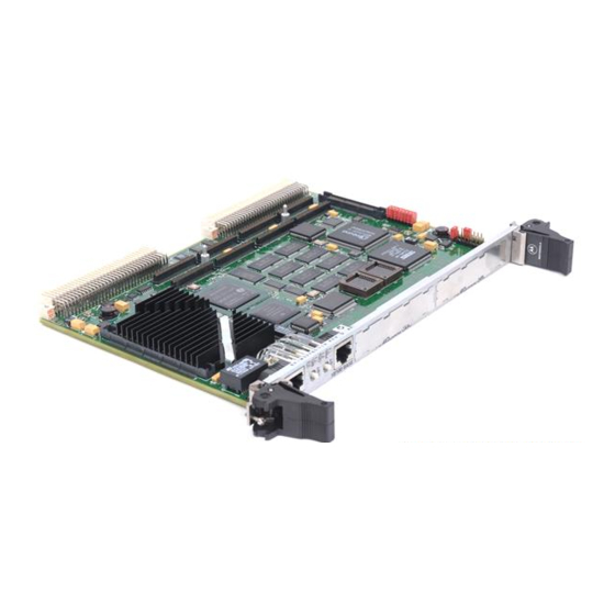
Page 25: Mvme230X
Preparing the MVME230x Hardware MVME 230x Figure 1-1. MVME230x Switches, LEDs, Headers, Connectors... -
Page 26: Setting The Flash Memory Bank A/Bank B Reset Vector Header (J15)
Preparing and Installing the MVME2300-Series Module Setting the Flash Memory Bank A/Bank B Reset Vector Header (J15) Bank B consists of 1 MB of 8-bit Flash memory in two 32-pin PLCC 8-bit sockets. Bank A consists of four 16-bit Smart Voltage SMT devices that can be populated with 8Mbit Flash devices (4 MB) or 4Mbit Flash devices (2 MB). -
Page 27: Setting The General-Purpose Software-Readable Header (J17)
Preparing the MVME230x Hardware Automatic System Controller System Controller Enabled System Controller Disabled (factory configuration) Setting the General-Purpose Software-Readable Header (J17) Header J17 provides eight readable jumpers. These jumpers can be read as a register at ISA I/O address $801 (hexadecimal). Bit 0 is associated with header pins 1 and 2;... -
Page 28: Pmcs
Preparing and Installing the MVME2300-Series Module PPCBug INSTALLED Bit 0 (SRH0) Reserved for future use Bit 1 (SRH1) Setup parameter source (In=Flash; Out=NVRAM) Bit 2 (SRH2) Reserved for future use Bit 3 (SRH3) Reserved for future use Bit 4 (SRH4) Reserved for future use Bit 5 (SRH5) Reserved for future use... -
Page 29: Installing The Mvme230X Hardware
MVME230x into a VME chassis, and connecting an optional system console terminal. Taking ESD Precautions Motorola strongly recommends that you use an antistatic wrist Use ESD strap and a conductive foam pad when installing or upgrading a system. Electronic components, such as disk drives, computer boards, and memory modules, can be extremely sensitive to Electro-Static Discharge (ESD). - Page 30 Preparing and Installing the MVME2300-Series Module 1. Attach an ESD strap to your wrist. Attach the other end of the ESD strap to the chassis as a ground. The ESD strap must be secured to your wrist and to ground throughout the procedure.
-
Page 31: Primary Pmcspan
Installing the MVME230x Hardware 2064 9708 Figure 1-3. Typical Single-width PMC Module Placement on MVME230x 5. Slide the edge connector(s) of the PMC module into the front panel opening(s) from behind and place the PMC module on top of the MVME230x. The four connectors on the underside of the PMC module should then connect smoothly with the corresponding connectors for a single-width PMC (J11/J12/J13/J14 or J21/J22/J23/J24, all eight for a double-... - Page 32 Preparing and Installing the MVME2300-Series Module was furnished with the PMCspan, and that you have installed the selected PMCs on the PMCspan according to the instructions given in the PMCspan and PMC manuals. 1. Attach an ESD strap to your wrist. Attach the other end of the ESD strap to the chassis as a ground.
-
Page 33: Figure 1-4. Pmcspan-002 Installation On An Mvme230X
Installing the MVME230x Hardware 2081 9708 Figure 1-4. PMCspan-002 Installation on an MVME230x 1-17... -
Page 34: Secondary Pmcspan
Preparing and Installing the MVME2300-Series Module 4. Attach the four standoffs to the MVME230x module. For each standoff: Ð Insert the threaded end into the standoff hole at each corner of the VME processor module. Ð Thread the locking nuts onto the standoff tips. Ð... -
Page 35: Figure 1-5. Pmcspan-010 Installation Onto A Pmcspan-002/Mvme230X
Installing the MVME230x Hardware 2065 9708 Figure 1-5. PMCspan-010 Installation onto a PMCspan-002/MVME230x 1-19... - Page 36 Preparing and Installing the MVME2300-Series Module 2. Perform an operating system shutdown. Turn the AC or DC power off and remove the AC cord or DC power lines from the system. Remove chassis or system cover(s) as necessary for access to the VME module card cage. Inserting or removing modules with power applied may result in damage to module components.
-
Page 37: Mvme230X
Installing the MVME230x Hardware MVME230 x Before installing the MVME230x into your VME chassis, ensure that the jumpers on the MVME230x J15, J16, and J17 headers are configured, as previously described. This procedure assumes that you have already installed the PMCspan(s) if desired, and any PMCs that you have selected. - Page 38 5. Secure the MVME230x (and PMCspans if used) in the chassis with the screws provided, making good contact with the transverse mounting rails to minimize RF emissions. Some VME backplanes (e.g., those used in Motorola Note ÒModular ChassisÓ systems) have an auto-jumpering feature for automatic propagation of the IACK and BG signals.
-
Page 39: Installation Considerations
Installing the MVME230x Hardware 8. Replace the chassis or system cover(s), cable peripherals to the panel connectors as appropriate, reconnect the system to the AC or DC power source, and turn the equipment power 9. The MVME230xÕs green LED indicates activity as a set of confidence tests is run, and the debugger prompt PPC1-Bug>... - Page 40 Preparing and Installing the MVME2300-Series Module Multiple MVME230x boards may be installed in a single VME chassis. Each must have a unique Universe address, selected by setting jumpers on its J17 header, as described in Preparing the MVME230x. In general, hardware multiprocessor features are supported.
-
Page 41: Introduction
2Operating Instructions Introduction This chapter provides information about powering up the MVME230x system, and functionality of the switches, status indicators, and I/O ports on the front panels of the MVME230x and PMCspan modules. Applying Power After you have verified that all necessary hardware preparation has been done, that all connections have been made correctly, and that the installation is complete, you can power up the system. -
Page 42: Mvme230X
Operating Instructions Power-up/reset initialization STARTUP Initialize devices on the MVME230x INITIALIZATION module/system Power On Self Test diagnostics POST Firmware-configured boot mechanism, BOOTING if so configured. Default is no boot. Interactive, command-driven on-line PowerPC MONITOR debugger, when terminal connected. MVME230 x The front panel of the MVME230x module is shown on a following page. -
Page 43: Abt (S1)
MVME230x ABT (S1) When activated by software, the Abort switch, , can generate an interrupt signal from the base board to the processor at a user- programmable level. The interrupt is normally used to abort program execution and return control to the debugger firmware located in the MVME230x Flash memory. -
Page 44: Status Indicators
Operating Instructions Status Indicators MVME There are four LED (light-emitting diode) status 230x indicators located on the MVME230x front panel.: , and BFL, CPU PMC2 PMC1 BFL (DS1) The yellow LED indicates board failure; lights when the BRDFAIL* signal line is active. CPU (DS2) The green LED indicates CPU activity;... -
Page 45: Debug Port
MVME230x DEBUG Port The RJ45 port labeled on the front panel of the MVME230x DEBUG supplies the MVME230x serial communications interface, implemented via a UART PC16550 controller chip from National Semiconductor. It is asynchronous only. This serial port is configured for EIA-232-D DTE, as shown in Figure 2-1. port may be used for connecting a terminal to the DEBUG MVME230x to serve as the firmware console for the factory... -
Page 46: Pmc Slots
Operating Instructions PMC Slots Two openings located on the front panel provide I/O expansion by allowing access to one or two 4-port single-wide or one 8-port double-wide PCI Mezzanine Card (PMC), connected to the PMC connectors on the MVME230x. For pin assignments for the PMC connectors, refer to Appendix C. -
Page 47: Pmcspan
PMCspan PMCspan A PMCspan front panel is pictured at the right. The front panel is the same for all PMCspan models. There are two PMC slots, labeled PCI MEZZANINE , which support either two single-wide PMCs CARD or one double-wide PMC. The PMCspan board has two sets of three 32-bit connectors for PMC interface to secondary PCI bus and user-specific I/O. - Page 48 Operating Instructions...
-
Page 49: Introduction
The following table summarizes the features of the MVME230x VME processor module. Table 3-1. MVME230x Features Feature Description 200 MHZ MPC603 PowerPC processor (MVME2301 - 2304 models) Microprocessor 300 MHZ MPC604 PowerPC processor (MVME2305 - 2308 models) Form factor 6U VMEbus... - Page 50 Features Table 3-1. MVME230x Features (Continued) Feature Description 8KB NVRAM with RTC and battery backup (SGS-Thomson Real-time clock M48T59/T559) Switches Reset ) and abort (RST (ABT) Status LEDs Four: Board fail (one for PMC slot 2, one for slot 1) (BFL) One 16-bit timer in W83C553 ISA bridge;...
-
Page 51: General Description
Functional Description General Description The MVME230x is a VME processor module equipped with a PowerPCª 603 or 604 microprocessor. As shown in the Features section, the MVME230x offers many standard features desirable in a computer systemÑincluding Ethernet and debug ports, Boot ROM, Flash memory, DRAM, and interface for two PCI Mezzanine Cards (PMCs), contained in a one- slot VME package. -
Page 52: Figure 3-1. Mvme230X Block Diagram
Block Diagram CLOCK DEBUG CONNECTOR GENERATOR DRAM 16/32/64/128MB FLASH PROCESSOR 3MB or 5MB MPC603/604 SYSTEM REGISTERS PHB & MPIC RAVEN ASIC MEMORY CONTROLLER FALCON CHIPSET 33MHz 32/64-BIT PCI LOCAL BUS VME BRIDGE W83C553 UNIVERSE ETHERNET DEC21140 RTC/NVRAM/WD BUFFERS MK48T59/559 PC16550 UART REGISTERS VME P2... -
Page 53: Pci Bus Latency
Functional Description The PowerPC 603 is a 64-bit processor with 16KB on-chip caches (16KB data cache and 16KB instruction cache). The PowerPC 604 is a 64-bit processor with 32 KB on-chip caches (32KB data cache and 32KB instruction cache). The Raven bridge controller ASIC provides the bridge between the PowerPC microprocessor bus and the PCI local bus. -
Page 54: Table 3-3. Powerpc 60X Bus To Pci Access Timing
Block Diagram The following table shows the access timings for various types of transfers initiated by a 60X system bus master to PCI: Table 3-3. PowerPC 60x Bus to PCI Access Timing System Clock Periods Required For: Total Access Type Clocks 1st Beat 2nd Beat... -
Page 55: Dram Memory
Functional Description Table 3-4. PCI to ECC Memory Access Timing PCI Clock Periods Required for: Maximum Access Type Bandwidth 1st Beat 2nd Beat 3rd Beat nth Beat 64-bit Burst Reads 64-bit Burst Writes 32-bit Burst Reads 32-bit Burst Writes 1-Beat Read 1-Beat Write Notes 1. -
Page 56: Dram Latency
Block Diagram There are one or two blocks of DRAMs that provides 16M/32M or 64M/128M of ECC DRAM. The DRAM blocks consists of 9 devices each. Either 1Mx16 (Page) 50-pin TSOPII DRAM or 4Mx16 (EDO) 50-pin TSOPII DRAM are used to provide 16/32/64/128M. When populated, these blocks appears as Block A and Block B to the Falcon chipset. -
Page 57: Table 3-5. Powerpc 60X Bus To Dram Access Timing Using 60Ns Page
Functional Description Table 3-5. PowerPC 60x Bus to DRAM Access Timing using 60ns Page Devices Clock Periods Required for: Total Access Type Clocks 1st Beat 2nd Beat 3rd Beat 4th Beat 4-Beat Read after Idle (Quad-word aligned) 4-Beat Read after Idle (Quad-word misaligned) 4-Beat Read after 4-Beat Read 11/7... -
Page 58: Table 3-6. Powerpc 60X Bus To Dram Access Timing Using 50Ns, Edo
Block Diagram If all blocks of DRAMs are 50ns, EDO devices then the latency times for the ECC memory would be as follows: Table 3-6. PowerPC 60x Bus to DRAM Access Timing Using 50ns, EDO Devices Clock Periods Required for: Total Access Type Clocks... -
Page 59: Flash Memory
Functional Description Flash Memory The MVME230x base board has provision for up to 5 MB of Flash memory. Bank B consists of 1 MB of 8-bit Flash memory in two 32-pin PLCC 8-bit sockets. Bank A consists of four 16-bit Smart Voltage SMT devices that can be populated with 8Mbit Flash devices (4 MB) or 4Mbit Flash devices (2 MB). -
Page 60: Flash Latency
Block Diagram Flash Latency There is one 16-bit port bank of Flash on the MVME230x. The access times for this bank are shown in the following table. Table 3-7.PowerPC 60x Bus to FLASH Access Timing for Bank B (16-bit Port) Clock Periods Required for: Total Access type... -
Page 61: Pci Mezzanine Card (Pmc) Interface
Functional Description 08003E2xxxxx is stored in NVRAM. The MVME230x debugger, PPCBug, has the capability to retrieve the Ethernet station address via the CNFG command. Note The unique Ethernet address is set at the factory and should not be changed. Any attempt to change this address may create node or bus contention and thereby render the board inoperable. -
Page 62: Pmc Slot 1 (Single-Width Pmc)
Block Diagram The MVME230x supports two PMC slots. Two sets of four 64-pin connectors on the base board (J11 - J14, and J21 - J24) interface with 32-bit/64-bit IEEE P1386.1 PMC-compatible mezzanines to add any desirable function. Refer to Appendix C for the pin assignments of the PMC connectors. -
Page 63: Pmc Slots 1 And 2 (Double-Width Pmc)
Functional Description For P2 I/O configurations, 46 I/O pins of PMC slot 2 are routed to the 5-row power adapter card. Pins 1 through 46 of J24 are routed to row D and row Z of P2. PMC Slots 1 and 2 (Double-Width PMC) PMC slots 1 and 2 with a double-width PMC have the following characteristics: Mezzanine Type... -
Page 64: Asynchronous Debug Port
Block Diagram programming information, refer to the Universe UserÕs Manual and to the discussions in the MVME2300-Series VME Processor Module Programmer's Reference Guide. Maximum performance is achieved with D64 Multiplexed Block Transfers (MBLT). The on-chip DMA channel should be used to move large blocks of data to/from the VMEbus. -
Page 65: Real-Time Clock/Nvram/Timer Function
Functional Description Ð ISA (Industry Standard Architecture) bus DMA (not functional on MVME230x) Ð The PHB (PCI Host Bridge) MPU/local bus interface function, implemented by the Raven ASIC Ð All on-board PCI devices Ð The PMC slot ISA bus arbitration for DMA devices ISA interrupt mapping for four PCI interrupts Interrupt controller functionality to support 14 ISA interrupts Edge/level control for ISA interrupts... -
Page 66: Pci Host Bridge
Block Diagram The SNAPHAT battery package is mounted on top of the M48T59/T559 device. The battery housing is keyed to prevent reverse insertion. The clock furnishes seconds, minutes, hours, day, date, month, and year in BCD 24-hour format. Corrections for 28-, 29- (leap year), and 30-day months are made automatically. -
Page 67: Programmable Timers
Functional Description Two software interrupts ISA interrupts (actually handles as a single 8259 interrupt at INT0) Programmable Timers Among the resources available to the local processor are a number of programmable timers. Timers are incorporated into the PCI/ISA Bridge (PIB) controller and the Raven device (diagrammed in Figure 3-1). - Page 68 Block Diagram periodic interrupts. For information on programming these timers, refer to the data sheet for the W83C553 PIB controller and to the MVME2300-Series VMe P:rocessor Module ProgrammerÕs Reference Guide. 3-20...
-
Page 69: Introduction
4Programming the MVME230x Introduction This chapter provides basic information useful in programming the MVME230x. This includes a description of memory maps, control and status registers, PCI arbitration, interrupt handling, sources of reset, and big/little endian issues. For additional programming information about the MVME230x, refer to the MVME2300-Series VME Processor Module ProgrammerÕs Reference Guide. -
Page 70: Processor Bus Memory Map
Programming the MVME230x Processor Bus Memory Map The processor memory map configuration is under the control of the Raven bridge controller ASIC and the Falcon memory controller chip set. The Raven and Falcon devices adjust system mapping to suit a given application via programmable map decoder registers. At system power-up or reset, a default processor memory map takes over. -
Page 71: Pci Local Bus Memory Map
Memory Maps For detailed processor memory maps, including suggested CHRP- and PREP-compatible memory maps, refer to the MVME2300-Series VME Processor Module ProgrammerÕs Reference Guide. PCI Local Bus Memory Map The PCI memory map is controlled by the Raven MPU/PCI bus bridge controller ASIC and by the Universe PCI/VME bus bridge ASIC. -
Page 72: Programming Considerations
Programming the MVME230x Programming Considerations Good programming practice dictates that only one MPU at a time have control of the MVME230x control registers. Of particular note are: Registers that modify the address map Registers that require two cycles to access VMEbus interrupt request registers PCI Arbitration There are seven potential PCI bus masters on the MVME230x :... -
Page 73: Figure 4-1. Vmebus Master Mapping
Programming Considerations VMEBUS PROCESSOR PCI MEMORY ONBOARD MEMORY PROGRAMMABLE SPACE NOTE 2 NOTE 1 PCI MEMORY SPACE VME A24 VME A16 NOTE 3 VME A24 VME A16 NOTE 1 VME A24 PCI/ISA MEMORY SPACE VME A16 VME A24 I/O SPACE VME A16 RESOURCES NOTES:... -
Page 74: Interrupt Handling
Programming the MVME230x The arbitration assignments for the MVME230x are shown in Table 4-2. Table 4-2. PCI Arbitration Assignments PCI Bus Request PCI Master(s) PIB (Internal) Raven ASIC Request 0 PMC Slot 2 Request 1 PMC Slot 1 Request 2 PCI Expansion Slot Request 3 Ethernet... -
Page 75: Figure 4-2. Mvme230X Interrupt Architecture
Programming Considerations INT_ Processor (8529 Pair) MCP_ RavenMPIC SERR_& PERR_ PCI Interrupts ISA Interrupts 11559.00 9609 Figure 4-2. MVME230x Interrupt Architecture The MVME230x routes the interrupts from the PMCs and PCI expansion slots as follows:... -
Page 76: Dma Channels
Programming the MVME230x PMC Slot 1 PMC Slot 2 PCIX Slot INTA# INTB# INTC# INTD# INTA# INTB# INTC# INTD# INTA# INTB# INTC# INTD# IRQ9 IRQ10 IRQ11 IRQ12 RavenMPIC DMA Channels The PIB supports seven DMA channels. They are not functional on the MVME230x. -
Page 77: Table 4-3. Classes Of Reset And Effectiveness
Programming Considerations 6. The VMEbus ∗ signal SYSRESET 7. VMEbus Reset sources from the Universe ASIC (PCI/VME bus bridge controller): the System Software reset, Local Software Reset, and VME CSR Reset functions Table 4-3 shows which devices are affected by the various types of resets. -
Page 78: Endian Issues
Programming the MVME230x Endian Issues The MVME230x supports both little-endian (e.g., Windows NT) and big-endian (e.g., AIX) software. The PowerPC processor and the VMEbus are inherently big-endian, while the PCI bus is inherently little-endian. The following sections summarize how the MVME230x handles software and hardware differences in big- and little-endian operations. -
Page 79: Vmebus Domain
Programming Considerations PCI and Ethernet Ethernet is byte-stream-oriented; the byte having the lowest address in memory is the first one to be transferred regardless of the endian mode. Since the Raven maintains address invariance in both little-endian and big-endian mode, no endian issues should arise for Ethernet data. - Page 80 Programming the MVME230x 4-12...
-
Page 81: Ppcbug Overview
Related Documentation appendix. PPCBug Basics The PowerPC debug firmware, PPCBug, is a powerful evaluation and debugging tool for systems built around the Motorola PowerPC microcomputers. Facilities are available for loading and executing user programs under complete operator control for system evaluation. - Page 82 PPCBug Basics Display and modification of memory Breakpoint and tracing capabilities A powerful assembler and disassembler useful for patching programs A self-test at power-up feature which verifies the integrity of the system PPCBug consists of three parts: A command-driven, user-interactive software debugger, described in the PPCBug Firmware Package UserÕs Manual.
-
Page 83: Memory Requirements
PPCBug Memory Requirements PPCBug requires a maximum of512KB of read/write memory (i.e., DRAM). The debugger allocates this space from the top of memory. For example, a system containing 64MB ($04000000) of read/write memory will place the PPCBug memory page at locations $03F80000 to $03FFFFFF. - Page 84 MPU, Hardware, and Firmware Initialization 7. Calculates the external bus clock speed of the MPU. 8. Delays for 750 milliseconds. 9. Determines the CPU base board type. 10. Sizes the local read/write memory (i.e., DRAM). 11. Initializes the read/write memory controller. Sets base address of memory to $00000000.
-
Page 85: Using Ppcbug
PPCBug 26. Verifies the configuration data that is resident in NVRAM, and displays a warning message if the verification failed. 27. Calculates and displays the MPU clock speed, verifies that the MPU clock speed matches the configuration data, and displays a warning message if the verification fails. 28. -
Page 86: Debugger Commands
Using PPCBug After the debugger executes the command, the prompt reappears. However, if the command causes execution of user target code (for example GO) then control may or may not return to the debugger, depending on what the user program does. For example, if a breakpoint has been specified, then control returns to the debugger when the breakpoint is encountered during execution of the user program. -
Page 87: Table 5-1. Debugger Commands
PPCBug Table 5-1. Debugger Commands Command Description One Line Assembler Block of Memory Compare Block of Memory Fill Block of Memory Initialize Block of Memory Move Breakpoint Insert NOBR Breakpoint Delete Block of Memory Search Block of Memory Verify Concurrent Mode NOCM No Concurrent Mode CNFG... - Page 88 Using PPCBug Table 5-1. Debugger Commands (Continued) Command Description Help IDLE Idle Master MPU I/O Control for Disk I/O Inquiry I/O Physical (Direct Disk Access) I/O Teach for ConÞguring Disk Controller Idle MPU Register Display Idle MPU Register Modify Idle MPU Register Set Load S-Records from Host Macro DeÞne/Display NOMA...
- Page 89 PPCBug Table 5-1. Debugger Commands (Continued) Command Description NOPA Printer Detach PBOOT Bootstrap Operating System Port Format NOPF Port Detach PFLASH Program FLASH Memory Put RTC into Power Save Mode ROMboot Enable NORB ROMboot Disable Register Display REMOTE Remote RESET Cold/Warm Reset Read Loop Register Modify...
-
Page 90: Diagnostic Tests
Using PPCBug Although a command to allow the erasing and reprogramming of Flash memory is available to you, keep in mind that reprogramming any portion of Flash Caution memory will erase everything currently contained in Flash, including the PPCBug debugger. Note, however, that both banks A and B of Flash contain the PPCBug debugger. -
Page 91: Table 5-2. Diagnostic Test Groups
PPCBug Table 5-2. Diagnostic Test Groups Test Group Description CL1283 Parallel Interface (CL1283) Tests* DEC21x40 Ethernet Controller Tests ISABRDGE PCI/ISA Bridge Tests KBD8730x PC8730x Keyboard/Mouse Tests* L2CACHE Level 2 Cache Tests* NCR 53C8xx SCSI-2 I/O Processor Tests* PAR8730x Parallel Interface (PC8730x) Test UART Serial Input/Output Tests PCIBUS... - Page 92 Using PPCBug 5-12...
-
Page 93: Overview
6Modifying the Environment Overview You can use the factory-installed debug monitor, PPCBug, to modify certain parameters contained in the MVME230x's Non- Volatile RAM (NVRAM), also known as Battery Backed-up RAM (BBRAM). The Board Information Block in NVRAM contains various elements concerning operating parameters of the hardware. Use the PPCBug command CNFG to change those parameters. -
Page 94: Cnfg - Conþgure Board Information Block
= “07” System Serial Number = “ nnnnnnn ” System Identifier = “Motorola MVME2300” License Identifier = “ nnnnnnnn “ The parameters that are quoted are left-justified character (ASCII) strings padded with space characters, and the quotes (Ò) are displayed to indicate the size of the string. Parameters that are not quoted are considered data strings, and data strings are right- justified. -
Page 95: Env - Set Environment
Modifying the Environment ENV - Set Environment Use the ENV command to view and/or configure interactively all PPCBug operational parameters that are kept in Non-Volatile RAM (NVRAM). Refer to the PPCBug Firmware Package User's Manual for a description of the use of ENV. Additional information on registers in the Universe ASIC that affect these parameters is contained in your MVME2300-Series VME Processor Module ProgrammerÕs Reference Guide. - Page 96 ENV - Set Environment Remote Start Method Switch [G/M/B/N] = B? The Remote Start Method Switch is used when the MVME2300 is cross-loaded from another VME-based CPU, to start execution of the cross-loaded program. Use the Global Control and Status Register to pass and start execution of the cross-loaded program.
- Page 97 Modifying the Environment Network PReP-Boot Mode Enable [Y/N] = N? Enable PReP-style network booting (same boot image from a network interface as from a mass storage device). Do not enable PReP-style network booting. (Default) Negate VMEbus SYSFAIL* Always [Y/N] = N? ∗...
- Page 98 ENV - Set Environment NVRAM Bootlist (GEV.fw-boot-path) Boot Enable [Y/N] = N? Give boot priority to devices deÞned in the fw- boot-path global environment variable (GEV). Do not give boot priority to devices listed in the fw-boot-path GEV. (Default) Note When enabled, the GEV (Global Environment Variable) boot takes priority over all other boots, including Autoboot and Network Boot.
- Page 99 Modifying the Environment Auto Boot Scan Enable [Y/N] = Y? If Autoboot is enabled, the Autoboot process attempts to boot from devices speciÞed in the scan list (e.g., FDISK/CDROM/TAPE/HDISK (Default) If Autoboot is enabled, the Autoboot process uses the Controller LUN and Device LUN to boot.
- Page 100 ENV - Set Environment Auto Boot Controller LUN = 00? Refer to the PPCBug Firmware Package User's Manual for a listing of disk/tape controller modules currently supported by PPCBug. (Default = $00) Auto Boot Device LUN = 00? Refer to the PPCBug Firmware Package User's Manual for a listing of disk/tape devices currently supported by PPCBug.
- Page 101 Modifying the Environment ROM Boot at power-up only [Y/N] = Y? ROMboot is attempted at power-up only. (Default) ROMboot is attempted at any reset. ROM Boot Enable search of VMEbus [Y/N] = N? VMEbus address space, in addition to the usual areas of memory, will be searched for a ROMboot module .
- Page 102 ENV - Set Environment Network Auto Boot Controller LUN = 00? Refer to the PPCBug Firmware Package User's Manual for a listing of network controller modules currently supported by PPCBug. (Default = $00) Network Auto Boot Device LUN = 00? Refer to the PPCBug Firmware Package User's Manual for a listing of network controller modules currently supported by PPCBug.
- Page 103 Modifying the Environment Memory Size Enable [Y/N] = Y? Memory will be sized for Self Test diagnostics. (Default) Memory will not be sized for Self Test diagnostics. Memory Size Starting Address = 00000000? The default Starting Address is $00000000. Memory Size Ending Address = 02000000? The default Ending Address is the calculated size of local memory.
- Page 104 ENV - Set Environment ROM Next Access Length (0 - 15) = 0? The value programmed into theÒROMNALÓ Þeld (Memory Control ConÞguration Register 8: bits 28-31) to represent wait states in access time for nibble (or burst) mode ROM accesses. The lowest allowable ROMNAL setting is $0;...
-
Page 105: Conþguring The Vmebus Interface
Modifying the Environment LED/Serial Startup Diagnostic Codes: these codes can Note be displayed at key points in the initialization of the hardware devices. Should the debugger fail to come up to a prompt, the last code displayed will indicate how far the initialization sequence had progressed before stalling. - Page 106 ENV - Set Environment PCI Slave Image 0 Bound Address Register = 00000000? The conÞgured value is written into the LSI0_BD register of the Universe chip. PCI Slave Image 0 Translation Offset = 00000000? The conÞgured value is written into the LSI0_TO register of the Universe chip.
- Page 107 Modifying the Environment PCI Slave Image 3 Control = C0400000? The conÞgured value is written into the LSI3_CTL register of the Universe chip. PCI Slave Image 3 Base Address Register = 2FFF0000? The conÞgured value is written into the LSI3_BS register of the Universe chip.
- Page 108 ENV - Set Environment VMEbus Slave Image 1 Bound Address Register = 00000000? The conÞgured value is written into the VSI1_BD register of the Universe chip. VMEbus Slave Image 1 Translation Offset = 00000000? The conÞgured value is written into the VSI1_TO register of the Universe chip.
- Page 109 Modifying the Environment PCI Miscellaneous Register = 10000000? The conÞgured value is written into the LMISC register of the Universe chip. Special PCI Slave Image Register = 00000000? The conÞgured value is written into the SLSI register of the Universe chip. Master Control Register = 80C00000? The conÞgured value is written into the MAST_CTL register of the Universe chip.
- Page 110 ENV - Set Environment 6-18...
-
Page 111: Motorola Computer Group Documents
PMCspan PMC Adapter Carrier Module Installation and Use PMCSPANA/IH Note Although not shown in the above list, each Motorola Computer Group manual publication number is suffixed with characters that represent the revision level of the document, such as Ò/xx2Ó (the second revision of a manual);... -
Page 112: Manufacturersõ Documents
Table A-2. Manufacturers’ Documents Publication Document Title and Source Number PowerPC 603 RISC Microprocessor Technical Summary MPC603/D Literature Distribution Center for Motorola Telephone: 1-800- 441-2447 FAX: (602) 994-6430 or (303) 675-2150 E-mail: ldcformotorola@hibbertco.com PowerPC 603 RISC Microprocessor UserÕs Manual MPC603UM/AD... - Page 113 Table A-2. Manufacturers’ Documents (Continued) Publication Document Title and Source Number PowerPC Microprocessor Family: The Programming Environments MPCFPE/AD Literature Distribution Center for Motorola Telephone: 1-800- 441-2447 FAX: (602) 994-6430 or (303) 675-2150 E-mail: ldcformotorola@hibbertco.com IBM Microelectronics Mail Stop A25/862-1 MPRPPCFPE-01...
- Page 114 Ordering Related Documentation Table A-2. Manufacturers’ Documents (Continued) Publication Document Title and Source Number W83C553 Enhanced System I/O Controller with PCI Arbiter (PIB) W83C553 Winbond Electronics Corporation Winbond Systems Laboratory 2730 Orchard Parkway San Jose, CA 95134 Telephone: (408) 943-6666 FAX:(408) 943-6668 M48T59 CMOS 8K x 8 TIMEKEEPER SRAM Data Sheet...
- Page 115 Related Specifications Related Specifications For additional information, refer to the following table for related specifications. As an additional help, a source for the listed document is also provided. Please note that in many cases, the information is preliminary and the revision levels of the documents are subject to change without notice.
- Page 116 Ordering Related Documentation Table A-3. Related Specifications (Continued) Publication Document Title and Source Number IEEE - PCI Mezzanine Card SpeciÞcation (PMC) P1386.1 Draft 2.0 Institute of Electrical and Electronics Engineers, Inc. Publication and Sales Department 345 East 47th Street New York, New York 10017-21633 Telephone: 1-800-678-4333 Bidirectional Parallel Port Interface SpeciÞcation IEEE Standard 1284...
- Page 117 Publication Document Title and Source Number PowerPC Microprocessor Common Hardware Reference Platform A System Architecture (CHRP), Version 1.0 Literature Distribution Center for Motorola Telephone: 1-800- 441-2447 FAX: (602) 994-6430 or (303) 675-2150 E-mail: ldcformotorola@hibbertco.com AFDA, Apple Computer, Inc. P. O. Box 319...
- Page 118 Ordering Related Documentation...
-
Page 119: Speciþcations
Specifications Specifications The following table lists the general specifications for the MVME230x VME processor module. The subsequent sections detail cooling requirements and EMC regulatory compliance. A complete functional description of the MVME230x boards appears in Chapter 3. Specifications for the optional PMCs can be found in the documentation for those modules. - Page 120 Specifications Table B-1. MVME230 x Specifications (Continued) Characteristics SpeciÞcations Relative humidity 10% to 80% Vibration (operating) 2 Gs RMS, 20Hz-2000Hz random Altitude (operating) 5000 meters (16,405 feet) Physical dimensions Height Double-high VME board, 9.2 in. (233 mm) (base board only) Front panel width 0.8 in.
-
Page 121: Cooling Requirements
(base board and modules) at a velocity typically achievable by using a 100 CFM axial fan. Temperature qualification is performed in a standard Motorola VMEsystem chassis. Twenty-five-watt load boards are inserted in two card slots, one on each side, adjacent to the board under test, to simulate a high power density system configuration. -
Page 122: Emc Regulatory Compliance
Specifications achieved with 10 CFM and 490 LFM flowing over the module. Less airflow is required to cool the module in environments having lower maximum ambients. Under more favorable thermal conditions, it may be possible to operate the module reliably at higher than 55û... -
Page 123: Introduction
Slot 2 64-bit PCI extension J23, J24 C-10 and P2 I/O Pin Assignments The following tables furnish pin assignments only. For detailed descriptions of the various interconnect signals, consult the support information documentation for the MVME230x (contact your Motorola sales office). -
Page 124: Vmebus Connector - P1
Connector Pin Assignments VMEbus Connector - P1 Two 160-pin DIN type connectors, P1 and P2, supply the interface between the base board and the VMEbus. P1 provides power and VME signals for 24-bit addressing and 16-bit data. Its pin assignments are set by the IEEE P1014-1987 VMEbus Specification and the VME64 Extension Standard. - Page 125 Pin Assignments Table C-1. P1 VMEbus Connector Pin Assignments (Continued) ∗ Not Used VIRQ6 VA13 Not Used ∗ VIRQ5 VA12 Not Used ∗ Not Used VIRQ4 VA11 Not Used ∗ VIRQ3 VA10 Not Used ∗ Not Used VIRQ2 Not Used ∗...
-
Page 126: Vmebus Connector - P2
Connector Pin Assignments VMEbus Connector - P2 Row B of the P2 connector provides power to the MVME230x, the upper eight VMEbus lines, and additional 16 VMEbus data lines as specified by the VMEbus specification Rows A, C, Z, and D of the P2 connector provide power and interface signals to a transition module, when one is used. - Page 127 Pin Assignments Table C-2. P2 Connector Pin Assignment (Continued) PMC2_35 (J24-35) PMC1_46 (J14-46) VD24 PMC1_45 (J14-45) PMC2_34 (J24-34) PMC1_48 (J14-48) VD25 PMC1_47 (J14-47) PMC2_36 (J24-36) PMC2_38 (J24-38) PMC1_50 (J14-50) VD26 PMC1_49 (J14-49) PMC2_37 (J24-37) PMC1_52 (J14-52) VD27 PMC1_51 (J14-51) PMC2_39 (J24-39) PMC2_41 (J24-41) PMC1_54 (J14-54) VD28...
-
Page 128: Serial Port Connector - Debug (J2
Connector Pin Assignments Serial Port Connector - DEBUG (J2) A standard RJ45 connector located on the front plate of the MVME230x provides the interface to the asynchronous serial debug port. The pin assignments for this connector are as follows: Table C-3. DEBUG (J2)Connector Pin Assignments Ethernet Connector - 10BASET (J3) The 10BaseT/100BaseTx connector is an RJ45 connector located on the front plate of the MVME230x. -
Page 129: Cpu Debug Connector - J1
Pin Assignments CPU Debug Connector - J1 One 190-pin Mictor connector with center row of power and ground pins is used to provide access to the Processor Bus and some miscellaneous signals. The pin assignments for this connector are as follows: Table C-5. - Page 130 Connector Pin Assignments Table C-5. Debug Connector Pin Assignments (Continued) PD10 PD11 PD12 PD13 PD14 PD15 PD16 PD17 PD18 PD19 PA20 PD21 PD22 PD23 PD24 PD25 PD26 PD27 PD28 PD29 PD30 PD31 PD32 PD33 PD34 PD35 PD36 PD37...
- Page 131 Pin Assignments Table C-5. Debug Connector Pin Assignments (Continued) PD38 PD39 PD40 PD41 PD42 PD43 PD44 PD45 PD46 PD47 PD48 PD49 PA50 PD51 PD52 PD53 PD54 PD55 PD56 PD57 PD58 PD59 PD60 PD61 PD62 PD63 PDPAR0 PDPAR1 PDPAR2 PDPAR3 PDPAR4 PDPAR5 PDPAR6 PDPAR7...
- Page 132 Connector Pin Assignments Table C-5. Debug Connector Pin Assignments (Continued) TSIZ0 TSIZ1 TSIZ2 CSE0 GLOBAL# CSE1 SHARED# DBWO# AACK# +3.3V ARTY# XATS# DRTY# TBST# TEA# DBG# DBB# ABB# TCLK_OUT CPUGNT0# CPUREQ0# C-10...
- Page 133 Pin Assignments Table C-5. Debug Connector Pin Assignments (Continued) CPUREQ1# INT0# CPUGNT1# MCPI# INT1# SMI# MCPI1# CKSTPI# L2BR# CKSTPO# L2BG# HALTED L2CLAIM# TLBISYNC# TBEN SUSPEND# DRVMOD0 DRVMOD1 NAPRUN SRESET1# QREQ# SRESET0# QACK# HRESET# CPUCLK CPUCLK CPUCLK TRST# C-11...
-
Page 134: Pci Expansion Connector - J18
Connector Pin Assignments PCI Expansion Connector - J18 One 114-pin Mictor connector with center row of power and ground pins is used to provide PCI/PMC expansion capability. The pin assignments for this connector are as follows: Table C-6. J18 - PCI Expansion Connector Pin Assignments +3.3V +3.3V PCICLK... - Page 135 Pin Assignments Table C-6. J18 - PCI Expansion Connector Pin Assignments (Continued) PCIRST# C/BE1# C/BE0# C/BE3# C/BE2# AD11 AD10 AD13 AD12 AD15 AD14 AD17 AD16 AD19 AD18 AD21 AD20 AD23 AD22 AD25 AD24 AD27 AD26 AD29 AD28 AD31 AD30 C-13...
- Page 136 Connector Pin Assignments Table C-6. J18 - PCI Expansion Connector Pin Assignments (Continued) PAR64 Reserved C/BE5# C/BE4# C/BE7# C/BE6# AD33 AD32 AD35 AD34 AD37 AD36 AD39 AD38 AD41 AD40 AD43 AD42 AD45 AD44 AD47 AD46 AD49 AD48 AD51 AD50 AD53 AD52 AD55 AD54...
-
Page 137: Pci Mezzanine Card Connectors - J11 Through J14
Pin Assignments PCI Mezzanine Card Connectors - J11 through J14 Four 64-pin SMT connectors, J11 through J14, supply 32/64-bit PCI interfaces and P2 I/O between the MVME230x board and an optional add-on PCI Mezzanine Card (PMC) in PMC Slot 1. The pin assignments for PMC Slot 1 are listed in the following two tables. -
Page 138: Table C-8. J13 - J14 Pmc1 Connector Pin Assignments
Connector Pin Assignments Table C-7. J11 - J12 PMC1 Connector Pin Assignments (Continued) 47 AD12 AD11 AD10 AD09 AD08 +3.3V C/BE0# AD07 Not Used AD06 AD05 +3.3V Not Used AD04 Not Used +5V (Vio) AD03 Not Used Not Used AD02 AD01 Not Used AD00... - Page 139 Pin Assignments Table C-8. J13 - J14 PMC1 Connector Pin Assignments (Continued) 33 GND AD48 PMC1_33 (P2-C17) PMC1_34 (P2-A17) 35 AD47 AD46 PMC1_35 (P2-C18) PMC1_36 (P2-A18) 37 AD45 PMC1_37 (P2-C19) PMC1_38 (P2-A19) 39 +5V (Vio) AD44 PMC1_39 (P2-C20) PMC1_40 (P2-A20) 41 AD43 AD42 PMC1_41 (P2-C21) PMC1_42 (P2-A21)
-
Page 140: Pci Mezzanine Card Connectors - J21 Through J24
Connector Pin Assignments PCI Mezzanine Card Connectors - J21 through J24 Four 64-pin SMT connectors, J21 through J24, supply 32/64-bit PCI interfaces and P2 I/O between the MVME230x board and an optional add-on PCI Mezzanine Card (PMC) in PMC Slot 2. The pin assignments for PMC Slot 2 are listed in the following two tables. -
Page 141: Table C-10. J23 And J24 Pmc2 Connector Pin Assignments
Pin Assignments Table C-9. J21 and J22 PMC2 Connector Pin Assignments (Continued) 47 AD12 AD11 47 GND AD10 49 AD09 +5V (Vio) 49 AD08 +3.3V 51 GND C/BE0# 51 AD07 Not Used 53 AD06 AD05 53 +3.3V Not Used 55 AD04 55 Not Used 57 +5V AD03... - Page 142 Connector Pin Assignments Table C-10. J23 and J24 PMC2 Connector Pin Assignments (Continued) 31 AD49 31 PMC2_31 (P2-D21) PMC2_32 (P2-Z21) 33 GND AD48 33 PMC2_33 (P2-D22 PMC2_34 (P2-D23) 35 AD47 AD46 35 PMC2_35 (P2-Z23) PMC2_36 (P2-D24) 37 AD45 37 PMC2_37 (P2-D25) PMC2_38 (P2-Z25 39 +5V (Vio) AD44...
-
Page 143: Solving Startup Problems
DTroubleshooting the MVME230x Solving Startup Problems In the event of difficulty with your MVME230x VME Processor Module, try the simple troubleshooting steps on the following pages before calling for help or sending the board back for repair. Some of the procedures will return the board to the factory debugger environment. -
Page 144: Table D-1. Troubleshooting Mvme230X Modules
Troubleshooting the MVME230x Table D-1. Troubleshooting MVME230x Modules Condition Possible Problem Try This: I. Nothing works, A. If the 1. Make sure the system is plugged in. no display on is not lit, the 2. Check that the board is securely installed in its backplane the terminal. - Page 145 Solving Startup Problems Table D-1. Troubleshooting MVME230x Modules (Continued) Condition Possible Problem Try This: III. Debug prompt A. Debugger Flash 1. Disconnect all power from your system. may be missing PPC1-Bug> 2. Check that the proper debugger devices are installedl. does not 3.
- Page 146 Troubleshooting the MVME230x Table D-1. Troubleshooting MVME230x Modules (Continued) Condition Possible Problem Try This: IV. Continued 2. At the command line prompt, type in: env;d <CR> This sets up the default parameters for the debugger environment. 3. When prompted to Update Non-Volatile RAM, type in: y <CR>...
- Page 147 Solving Startup Problems Table D-1. Troubleshooting MVME230x Modules (Continued) Condition Possible Problem Try This: V. The debugger is A. No apparent No further troubleshooting steps are required. in system mode problems Ñ and the board troubleshooting autoboots, or is done. the board has passed selftests.
- Page 148 Troubleshooting the MVME230x...
-
Page 149: Abbreviations, Acronyms, And Terms To Know
Glossary Abbreviations, Acronyms, and Terms to Know This glossary defines some of the abbreviations, acronyms, and key terms used in this document. An Ethernet implementation in which the physical medium 10Base-5 is a doubly shielded, 50-ohm coaxial cable capable of carrying data at 10 Mbps for a length of 500 meters (also referred to as thicknet). - Page 150 Glossary Application-Specific Integrated Circuit ASIC Attachment Unit Interface Battery Backed-up Random Access Memory BBRAM Having big-endian and little-endian byte ordering bi-endian capability. A byte-ordering method in memory where the address big-endian n of a word corresponds to the most significant byte. In an addressed memory word, the bytes are ordered (left to right) 0, 1, 2, 3, with 0 being the most significant byte.
- Page 151 The Green signals (G-Y) can be extracted by these two signals. Common Hardware Reference Platform (CHRP) A specification published by Apple, IBM, and Motorola which defines the devices, interfaces, and data formats that make up a CHRP-compliant system using a PowerPC processor.
- Page 152 Glossary Central Processing Unit. The master computer unit in a system. Data Circuit-terminating Equipment. Dynamic Link Library. A set of functions that are linked to the referencing program at the time it is loaded into memory. Direct Memory Access. A method by which a device may read or write to memory directly without processor intervention.
- Page 153 A local area network standard that uses radio frequency Ethernet signals carried by coaxial cables. The DRAM controller chip developed by Motorola for the Falcon MVME2600 and MVME3600 series of boards. It is intended to be used in sets of two to provide the necessary interface between the Power PC60x bus and the 144-bit ECC DRAM (system memory array) and/or ROM/Flash.
- Page 154 Glossary A computing system is normally spoken of as having two hardware major components: hardware and software. Hardware is the term used to describe any of the physical embodiments of a computer system, with emphasis on the electronic circuits (the computer) and electromechanical devices (peripherals) that make up the system.
- Page 155 Multimedia Personal Computer The PowerPC-to-PCI bus bridge chip developed by MPC105 Motorola for the Ultra 603/Ultra 604 system board. It provides the necessary interface between the MPC603/ MPC604 processor and the Boot ROM (secondary cache), the DRAM (system memory array), and the PCI bus.
- Page 156 Glossary several different ways, yielding substantially different results. The specification is based on a large number of samplings in one place, running continuously, and the rate at which failure occurs. MTBF is not representative of how long a device, or any individual device is likely to last, nor is it a warranty, but rather, a gauge of the relative reliability of a family of products.
- Page 157 (branch units, fixed-point units, and floating-point units), where they can execute concurrently, but finish out of order. PowerPC is used by Motorola, Inc. under license from IBM. The first implementation of the PowerPC family of PowerPC 601™...
- Page 158 64-entry buffer and an 8KB (instruction and data) cache. It provides a selectable 32-bit or 64-bit data bus and a separate 32-bit address bus. PowerPC 603 is used by Motorola, Inc. under license from IBM. The third implementation of the PowerPC family of PowerPC 604™...
- Page 159 Glossary The PowerPC-to-PCI local bus bridge chip developed by Raven Motorola for the MVME2600 and MVME3600 series of boards. It provides the necessary interface between the PowerPC 60x bus and the PCI bus, and acts as interrupt controller. Reduced-Instruction-Set Computer (RISC) A computer in which the processorÕs instruction set is...
- Page 160 Glossary Super I/O controller Symmetric MultiProcessing. A computer architecture in which tasks are distributed among two or more local processors. Surface Mount Technology. A method of mounting devices (such as integrated circuits, resistors, capacitors, and others) on a printed circuit board, characterized by not requiring mounting holes.
- Page 161 Glossary ASIC developed by Tundra in consultation with Motorola, Universe that provides the complete interface between the PCI bus and the 64-bit VMEbus. UltraViolet Ultra Video Graphics Array. An improved VGA monitor UVGA standard that provides at least 256 simultaneous colors and a screen resolution of 1024 x 768 pixels.
- Page 162 Glossary port for CPU accesses. The result of adding the serial port is a significantly reduced amount of interference from screen refresh. VRAMs cost more per bit than DRAMs. The trademark representing Windows New Technology, a Windows NT™ computer operating system developed by the Microsoft Corporation.
- Page 163 Index Numerics configurations MVME230x 10/100 BASET port configure 16/32-bit timers 3-19 PPC1Bug parameters VMEbus interface 6-13 Configure Board Information Block abbreviations, acronyms, and terms to (CNFG) know GL-1 configuring the hardware abort (interrupt) signal connector pin assignments ABT switch (S1) console terminal address pipelining 3-9, 3-10...
- Page 164 Index EMC regulatory compliance HE (Help) command 5-10 endian issues headers function of Raven ASIC 4-10 1-10 function of Universe ASIC 4-11 1-10 PCI domain 4-10 1-11 processor/memory domain 4-10 help command 5-10 VMEbus domain 4-11 humidity, relative ENV command environmental parameters IACK and BG signals 1-22...
- Page 165 MVME230x PCI-ISA Bridge (PIB) controller 3-16 VMEbus PCI-ISA bridge controller (PIB) memory size 6-11 functions 3-16 Motorola Computer Group documents Peripheral Computer Interface (PCI) MPC603/604 processor PHB (PCI Host Bridge) 3-18 MPIC (MultiProcessor Interrupt PIB controller 3-16, 4-4 Controler) 3-18...
- Page 166 Index preparing 1-12 restart mode 5-11 PMCspan RF emissions preparing 1-12 ROMboot enable 6-8, 6-12 PMCspan Expansion Mezzanine ROMFAL 6-11 PMCspan-002 Installation on an ROMNAL 6-12 MVME230x 1-17 port SCSI bus asynchronous 3-16 SD command 5-10 debug 3-16 secondary PMCspan port, Ethernet installing 1-18...
- Page 167 Index 16/32-bit 3-19 interval 3-19 timers, programmable 3-19 timers, via Universe chip timing owerPC bus to DRAM PCI to ECC memory PowerPC bus to DRAM troubleshooting procedures troubleshooting the MVME230x 5-10 Typical Single-width PMC Module Placement on MVME230x 1-15 Universe VMEbus interface ASIC 2-3, 3-15, 4-3, 4-4, 4-9, 4-11 unpacking the hardware...