Table of Contents
Advertisement
Quick Links
Advertisement
Table of Contents

Related Manuals for Motorola MVME3100


Summary of Contents for Motorola MVME3100
- Page 1 MVME3100 Single-Board Computer Programmer’s Guide V3100A/PG1 March 2006 Edition...
- Page 2 All rights reserved. Printed in the United States of America. Motorola and the stylized M logo are trademarks of Motorola, Inc., registered in the U.S. Patent and Trademark Office. All other product or service names mentioned in this document are the property of their...
- Page 3 The safety precautions listed below represent warnings of certain dangers of which Motorola is aware. You, as the user of the product, should follow these warnings and all other safety precautions necessary for the safe operation of the equipment in your operating environment.
- Page 4 Flammability All Motorola PWBs (printed wiring boards) are manufactured with a flammability rating of 94V-0 by UL-recognized manufacturers. EMI Caution This equipment generates, uses and can radiate electromagnetic energy. It Caution may cause or be susceptible to electromagnetic interference (EMI) if not installed and used with adequate EMI protection.
- Page 5 Warning Motorola products with the CE marking comply with the EMC Directive (89/336/EEC). Compliance with this directive implies conformity to the following European Norms: EN55022 “Limits and Methods of Measurement of Radio Interference Characteristics of Information Technology Equipment”;...
- Page 6 Electronic versions of this material may be read online, downloaded for personal use, or referenced in another document as a URL to the Motorola Web site. The text itself may not be published commercially in print or electronic form, edited, translated, or otherwise altered without the permission of Motorola, Inc.
-
Page 7: Table Of Contents
RTM VPD EEPROM ..............31 MVME3100 Programmer’s Guide (V3100A/PG1) - Page 8 Motorola Computer Group Documents ........
-
Page 9: List Of Figures
Figure 1-1. MVME3100 Block Diagram ........ - Page 10 Table A-1. Motorola Computer Group Documents ........
-
Page 11: About This Manual
The MVME3100 Single-Board Computer Programmer’s Reference Guide provides general programming information, including memory maps, interrupts, and register data for the MVME3100 family of boards. This document should be used by anyone who wants general, as well as technical information about the MVME3100 products. -
Page 12: Conventions Used In This Manual
(for example, screen displays, reports), examples, and system prompts. <Enter>, <Return> or <CR> represents the carriage return or Enter key. Ctrl represents the Control key. Execute control characters by pressing the Ctrl key and the letter simultaneously, for example, Ctrl-d. MVME3100 Programmer’s Guide (V3100A/PG1) -
Page 13: Board Description And Memory Maps
Board Description and Memory Maps Introduction This chapter briefly describes the board level hardware features of the MVME3100 single-board computer, including a table of features and a block diagram. The remainder of the chapter provides memory map information including a default memory map, MOTLoad’s processor memory map, a default PCI memory map, MOTLoad’s PCI memory map, system I/O memory map, and other... -
Page 14: Front Panel
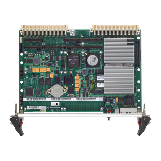
Chapter 1 Board Description and Memory Maps Figure 1-1. MVME3100 Block Diagram Front Panel RST/ABORT GigE COM1 PMC 1 Front IO PMC 2 Front IO RJ45 RJ45 sATA 166 MHz Memory Bus XCVR SODIMM - Up to RS232 1GB DDR Memory... -
Page 15: Table 1-1. Mvme3100 Features Summary
Chapter 1 Board Description and Memory Maps Table 1-1. MVME3100 Features Summary Feature Description Processor/Host – Single 667/833 MHz MPC8540 PowerQUICC III™ integrated Controller/Memory processor (e500 core) Controller – Integrated 256KB L2 cache/SRAM – Integrated four-channel DMA controller – Integrated PCI/PCI-X controller –... - Page 16 Chapter 1 Board Description and Memory Maps Table 1-1. MVME3100 Features Summary (continued) Feature Description Serial ATA – One four-channel sATA controller: one channel for front-panel I/O, one channel for planar I/O, one channel for future rear P0 I/O, and one channel is not used –...
-
Page 17: Memory Maps
Table 1-2. MVME712-101 RTM Features Summary Feature Description – One five-row P2 backplane connector for serial and Ethernet I/O passed from the MVME3100 – Four RJ-45 connectors for rear-panel I/O: four asynchronous serial channels – Two RJ-45 connectors with integrated LEDs for rear panel I/O:... -
Page 18: Motload's Processor Memory Map
After RESET, the MPC8540 does not map any PCI memory space (inbound or outbound), and does not respond to Config cycles. VME Memory Map The MVME3100 is fully capable of supporting both the PReP and the CHRP VME Memory Map examples with RAM size limited to 2GB. MVME3100 Programmer’s Guide (V3100A/PG1) -
Page 19: System I/O Memory Map
System resources including System Control and Status registers, external timers, and the QUART are mapped into a 16MB address range from the MVME3100 via the MPC8540 local bus controller (LBC). The memory map is defined in the following table, including the LBC bank chip select used to decode the register: Table 1-5. - Page 20 External PLD Tick Timer 4 Compare Register E202 0048 External PLD Tick Timer 4 Counter Register E202 004C - Reserved E2FF FFFF Notes 1. Reserved for future implementation 2. 32-bit write only 3. Byte read/write capable MVME3100 Programmer’s Guide (V3100A/PG1)
-
Page 21: System Status Register
Chapter 1 Board Description and Memory Maps System Status Register The MVME3100 board System Status register is a read-only register used to provide board status information. Table 1-6. System Status Register System Status Register – 0xE2000000 FIELD OPER RESET BD_TYPE Board type. -
Page 22: System Control Register
Chapter 1 Board Description and Memory Maps System Control Register The MVME3100 board System Control register provides board control bits. Table 1-7. System Control Register System Control Register - 0xE2000001 FIELD OPER RESET TSTAT_MASK Thermostat mask. This bit masks the DS1621 temperature sensor thermostat output. If this bit is cleared, the thermostat output is enabled to generate an interrupt. -
Page 23: System Indicator Register
Chapter 1 Board Description and Memory Maps System Indicator Register The MVME3100 board provides a System Indicator register that may be read by the system software to determine the state of the on-board status indicator LEDs or written to by system software to illuminate the corresponding on-board LEDs. -
Page 24: Flash Control/Status Register
Chapter 1 Board Description and Memory Maps Flash Control/Status Register The MVME3100 provides software-controlled bank write protect and map select functions as well as boot block select, bank write protect, and activity status for the Flash. Table 1-9. Flash Control/Status Register... -
Page 25: Pci Bus Status Registers
PCI-X mode. A cleared condition indicates PCI mode. PCI_A_64B PCI bus A 64-bit. A set condition indicates that bus A is enabled to operate in 64-bit mode. A cleared condition indicates 32-bit mode. RSVD Reserved for future implementation. MVME3100 Programmer’s Guide (V3100A/PG1) -
Page 26: Table 1-11. Pci Bus B Status Register
5.0V VIO Enabled. This bit set indicates that the PMC bus (PCI bus B) is configured for 5.0V VIO. 3.3V_VIO 3.3V VIO enabled. This bit set indicates that the PMC bus (PCI bus B) is configured to 3.3V VIO. MVME3100 Programmer’s Guide (V3100A/PG1) -
Page 27: Table 1-12. Pci Bus C Status Register
PCI-X mode. A cleared condition indicates PCI mode. PCI_C_64B PCI bus C 64-bit. A set condition indicates that bus C is enabled to operate in 64-bit mode. A cleared condition indicates 32-bit mode. RSVD Reserved for future implementation. MVME3100 Programmer’s Guide (V3100A/PG1) -
Page 28: Interrupt Detect Register
Chapter 1 Board Description and Memory Maps Interrupt Detect Register The MVME3100 provides an Interrupt Detect register that may be read by the system software to determine which of the Ethernet PHYs originated their combined (OR’d) interrupt. Table 1-13. Interrupt Detect Register... -
Page 29: Presence Detect Register
Chapter 1 Board Description and Memory Maps Presence Detect Register The MVME3100 provides a Presence Detect register that may be read by the system software to determine the presence of optional devices. Table 1-14. Presence Detect Register Presence Detect Register - 0xE2000008... -
Page 30: Pld Revision Register
Chapter 1 Board Description and Memory Maps PLD Revision Register The MVME3100 provides a PLD Revision register that may be read by the system software to determine the current revision of the timers/registers PLD. Table 1-15. PLD Revision Register PLD Revision Register - 0xE2000009... -
Page 31: Test Register 1
0000 TEST1 General-purpose 32-bit read/write field. Test Register 2 The MVME3100 provides a second 32-bit test register that reads back the complement of the data in test register 1. Table 1-18. Test Register 2 Test Register 2 - 0xE2000014 31:0... -
Page 32: Prescalar Register
Tick Timer 3 Control Register - 0xE2020030 (32 bits) Tick Timer 4 Control Register - 0xE2020040 (32 bits) FIELD OPER RESET Enable counter. When this bit is high, the counter increments. When this bit is low, the counter does not increment. MVME3100 Programmer’s Guide (V3100A/PG1) -
Page 33: Compare Registers
If the clear-on-compare mode is enabled, the counter is also cleared. For periodic interrupts, this equation should be used to calculate the compare register value for a specific period (T): Compare register value = T (us) MVME3100 Programmer’s Guide (V3100A/PG1) -
Page 34: Counter Registers
Geographical Address Register The VMEbus Status register in the TSi148 provides the VMEbus geographical address of the MVME3100. This register reflects the inverted states of the geographical address pins at the 5-row, 160- pin P1 connector. MVME3100 Programmer’s Guide (V3100A/PG1) -
Page 35: Programming Details
Programming Details Introduction This chapter includes additional programming information for the MVME3100 single-board computer. Items discussed include: ■ MPC8540 Reset Configuration on page 24 ■ MPC8540 Interrupt Controller on page 28 ■ Local Bus Controller Chip Select Assignments on page 29 ■... -
Page 36: Mpc8540 Reset Configuration
Chapter 2 Programming Details MPC8540 Reset Configuration The MVME3100 supports the power-on reset (POR) pin sampling method for MPC8540 reset configuration. The states of the various configuration pins on the MPC8540 are sampled when reset is de-asserted to determine the desired operating modes. The following table describes the configuration options and the corresponding default setting. - Page 37 (0 added buffer delays for LALE) TSEC2_ Fixed RapidIO Device ID Unconnected Inputs TXD [2:4] (3 lower-order bits) LA27 Resistor CPU Boot CPU boot hold off Configuration mode e500 core boots without waiting for configuration by an external master MVME3100 Programmer’s Guide (V3100A/PG1)
- Page 38 Core : CCB Clock) LGPL0, LGPL1 Fixed RapidIO Transmit Reserved Clock Source RapidIO rcv clock is source of xmit clock RapidIO xmit clock inputs are source of xmit clock CCB clock is source of xmit clock MVME3100 Programmer’s Guide (V3100A/PG1)
- Page 39 6. Meets 0.7 ns hold time requirement. 7. Local bus LAD[0:31] is sampled during POR, but only LAD[28:31] are configurable by resistor option. Software can use this value to inform the firmware or operating system about initial board configuration. MVME3100 Programmer’s Guide (V3100A/PG1)
-
Page 40: Mpc8540 Interrupt Controller
8. ECC signals from memory devices must be disconnected. MPC8540 Interrupt Controller The MVME3100 uses the MPC8540 integrated programmable interrupt controller (PIC) to manage locally generated interrupts. Currently defined external interrupting devices and interrupt assignments, along with corresponding edge/levels and polarities, are shown in the following table. -
Page 41: Local Bus Controller Chip Select Assignments
3. 32-bit timer registers are byte readable, but must be written as 32 bits. Two-Wire Serial Interface A two-wire serial interface for the MVME3100 is provided by an I C compatible serial controller integrated into the MPC8540. The MPC8540 I... -
Page 42: User Configuration Eeprom
MVME3100 is $AA. User Configuration EEPROM The MVME3100 board provides two 64KB dual address serial EEPROMs for a total of 128KB user configuration storage. These EEPROMs are hardwired to have device IDs as shown in Table 2-4 on page 29, and each device ID will not be used for any other function. -
Page 43: Rtm Vpd Eeprom
MVME3100 RTM. Typical information that may be present in the EEPROM may include: manufacturer, board revision, build version, date of assembly, options present, etc. The RTM VPD EEPROM device ID is user selectable with the recommended value for MVME3100 as shown Table 2-4 on page 29. -
Page 44: Pci Idsel Definition
F_WP_SW bit supports both read and write operations. The MVME3100 provides a dual boot option for booting from one of two separate boot images in the boot Flash bank, which are referred to as boot block A and boot block B. Boot blocks A and B are each 1MB in size and are located at the top (highest address) 2 MB of the boot Flash memory space. -
Page 45: Table 2-8. Planar Pci Device Identification
Table 2-8. Planar PCI Device Identification Function Device Vendor ID Device ID System Controller MPC8540 0x1057 0x0008 PCI-X-to-PCI-X Bridge PCI6520CB 0x10B5 0x6520 VME Controller TSi148 0x10E3 0x0148 sATA Controller GD31244 0x8086 0x3200 USB Controller µPD720101 0x1033 0x0035 MVME3100 Programmer’s Guide (V3100A/PG1) -
Page 46: Pci Arbitration Assignments
PCI6520. One secondary arbiter provides arbitration for the PMC sites on PCI bus B, and the other provides arbitration for the PMCspan and USB host controller on PCI bus C. The arbitration assignments on the MVME3100 are shown in the follow table so that software may set arbiter priority assignments if necessary. -
Page 47: Table 2-10. Clock Assignments
CLK25_33V_PHY Oscillator/ 3.3V Buffer Control and CLK25_33V_PLD Oscillator/ 3.3V Timers PLD Buffer CLK_LBC CCB_CLK/8 MPC8540 3.3V (333 MHz/8) QUART CLK_UART 1.8432 Oscillator 3.3V sATA CLK37 37.5 Oscillator 3.3V CLK48 Oscillator 3.3V CLK32 32.768 kHz Crystal 3.3V MVME3100 Programmer’s Guide (V3100A/PG1) -
Page 48: Mpc8540 Real-Time Clock Input
2, 4 or 8 ratio of the internal CCB (core complex bus) clock as determined by the clock ratio register (LCRR[CLKDIV]). For proper operation of the local bus, CLKDIV must be set for divide by 8, which is the default value. The software must leave this register configured for divide by 8 during initialization. MVME3100 Programmer’s Guide (V3100A/PG1) -
Page 49: Motorola Computer Group Documents
Related Documentation Motorola Computer Group Documents The Motorola publications listed below are referenced in this manual. You can obtain electronic copies of Motorola Computer Group publications by: ■ Contacting your local Motorola sales office ■ Visiting Motorola Computer Group’s World Wide Web literature site, http://www.motorola.com/computer/literature... -
Page 50: Manufacturers' Documents
Table A-2. Manufacturers’ Documents Document Title and Source Publication Number MPC8540 Microprocessor Hardware Specification MPC8540 Literature Distribution Center for Motorola Telephone: 1-800- 441-2447 FAX: (602) 994-6430 or (303) 675-2150 Web Site: http://e-www.motorola.com/webapp/sps/library/prod_lib.jsp E-mail: ldcformotorola@hibbertco.com MPC8540 PowerQUICC III™ Integrated Host Processor Reference MPC8540RMRev. - Page 51 Maxim DS1621Digital Thermometer and Thermostat DS1621 Maxim Integrated Products Web Site: http://www.maxim-ic.com Maxim DS1375 Serial Real-Time Clock REV: 121203 Maxim Integrated Products Web Site: http://www.maxim-ic.com TSOP Type I Shielded Metal Cover SMT Yamaichi Electronics USA Web Site: http://www.yeu.com MVME3100 Programmer’s Guide (V3100A/PG1)
-
Page 52: Related Specifications
P1386 Draft 2.0 Electrical and Electronics Engineers, Inc. IEEE - PCI Mezzanine Card Specification (PMC) P1386.1 Draft 2.0 Institute of Electrical and Electronics Engineers, Inc. USB http://www.usb.org/developers/docs/ Universal Serial Bus Specification Revision 2.0 April 27, 2000 MVME3100 Programmer’s Guide (V3100A/PG1)