Table of Contents
Advertisement
Advertisement
Table of Contents

Related Manuals for Zoom g9.2tt


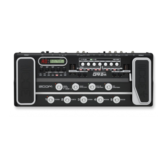
Summary of Contents for Zoom g9.2tt
-
Page 2: Table Of Contents
Circuit Diagram ............................28 Exploded view ............................43 Parts List ..............................44 Spare Parts Order List ..........................51 Spare Parts Order Sheet ..........................56 Supplement 1: G9.2tt optical sensor problem..................57 Supplement 2: G9.2tt PEDAL SW Adjustment specifications..............61 Importance: Harness Fixing........................63 - 2 -... -
Page 3: Specifications
Specifications 106 types Number of effect types 10 simultaneously usable modules Number of effect modules User area : 5 patches x 20 banks = 100 (read/write enabled) Patch memory Preset area : 5 patches x 20 banks = 100 (read only)Total: 200 patches 96 kHz Sampling frequency... - Page 4 Outputs Standard monaural phone jack x 2 Line output Rated output level: -10 dBm/+4 dBm (switchable) Maximum output level: +19 dBm (into load impedance of 10 kilohms or more) Output impedance: 1 kilohm or less Standard stereo phone jack Headphone output Rated output: 60 m W (into 32-ohm load), 20 m W (into 300-ohm load) Output impedance: 47 ohm...
-
Page 5: Function Test
Function Test After the G9.2tt is assembled, the following inspections and settings should be made. * Equipment required · AC voltage meter (audio analyzer would be better) · IHF-A filter (audio analyzer might include it) · Oscillator · AC adapter (AD-00012) ·... - Page 6 2. GAIN SW check Following the operation “1.”, input sin wave (440Hz/-20dBm) to [INPUT] jack and monitor the output from [OUTPUT] jack (L/MONO, R) with speakers and oscilloscope. Make sure that output level changes by switching [-10dBm] and [+4dBm]. Then, output from [Phones] jack doesn’t change.
- Page 7 6. SEND / RETURN check Input sin wave (440Hz/-20dBm) to [INPUT] jack and [RETURN] jack, and monitor the output from [OUTPUT] jack (L/MONO, R) with speakers and oscilloscope. Then, insert to [RETURN] jack and pull from [RETURN] jack, and make sure that the LCD display indicates [RETURN plugged].
- Page 8 10. ANALOG-MUTE check Press the [STORE/SWAP] key (SW16). Make sure that the [STORE/SWAP] key lights red, and LCD is displayed [STORE/SWAP ANALOG MUTE]. The 7segment LED turns [on] and [oF] by pressing the [STORE/SWAP] key. When the 7segment LED turns on, sound from [PHONE] jack, [L/MONO] jack, [R] jack, and [SEND] jack are extremely low.
- Page 9 14. MIDI LOOPBACK check Connect MIDI cable to [MIDI IN] and [MIDI OUT] (J401) PUSH [HOLD MANUAL BANK↓] FOOT SW (SW22). [HOLD MANUAL BANK↓] LED lights red. LCD displays [MIDI LOOPBACK]. Confirmation of data transmission will be done. If transmission is OK, LCD displays [MIDI LOOPBACK Success], 7 segment LED displays [ok]. Otherwise, LCD displays [MIDI LOOPBACK 00 timeouted], 7 segment LED displays [nG].
- Page 10 19. INPUT CIRCUIT NOISE check Push [PRE-AMP] FOOT SW (SW23) [PRE-AMP] key lights red. LCD displays [GAIN +60]. About this check, adjust [TUBE] of ACCELERATOR, [SOLID STATE] of ACCELERATOR, [TUBE] of ENERGIZER, and [BOOST] of ENERGIZER to 5. Make sure that noise level increases. When 7 segment LED displays [on], DSP has +60dB gain and increase white noise of [OUTPUT] jack (PHONE, L/MONO, R jack) and [SEND] jack sound.
- Page 11 23. EX PEDAL1 check The 7segment LED is displayed EX PEDAL’s AD value if the PEDAL is moved. Make sure that this EX PEDAL’s AD value is the same as below table and LCD displayed [PEDAL2-V]. *MIN : raise EX PEDAL this side. *MAX : lower EX PEDAL till that contacts gum lightly.
- Page 12 27. EX PEDAL2 / Z PEDAL check The 7segment LED is displayed vertical AD value of EX PEDAL2 if the PEDAL is moved vertically. Make sure that this AD value of EX PEDAL is the same as below table and LCD displayed [PEDAL1].
- Page 13 29. PEDAL setting Turn on the power holding the [PEDAL2 SETTING] key, and the indication [PDL Calibration PEDAL2-V…min] appears on the LCD. With the EX PEDAL2 fully raised, press the [STORE/SWAP] key, and the indication [PDL Calibration PEDAL2-V…MAX] appears on the LCD.
- Page 14 33. ACCELERATOR check Turn the [SOLOD STATE] knob and the [TUBE] knob counterclockwise extremely, and output sound from all [OUTPUT] jacks will be muted. Turn the [SOLID STATE] knob clockwise, and output sound from all [OUTPUT] jacks will be louder. Turn the [SOLID STATE] knob counterclockwise again, and turn the [TUBE] knob clockwise, and output sound from all [OUTPUT] jacks will be distorted and louder.
- Page 15 *Refer to “How to use USB inspection software” about the how to use inspection software. 41. Stability Put the G9.2tt on a surface plate, and push it diagonally. Make sure that there is no remarkable space (less than ±0.7 mm is acceptable).
- Page 16 42. Factory default setting Set the knobs and switch as follows: OUTPUT VOLUME Center All EFFECT VOLUME Turn anticlockwise till limit All ENERGIZER VOLUME Turn anticlockwise till limit TUBE VOLUME OF ACCELERATOR Adjust to 5 (center) SOLID STATE VOLUME OF ACCELERATOR Adjust to 5 (center) GAIN SW (both OUTPUT and EXT LOOP) -10 dBm...
-
Page 17: Tube Adjustment Specification
Tube Adjustment Specification 1. Overview This specification describes the method to adjust differences due to characteristics of tubes. 2. ACCELERATOR (Input side) adjustment There are two methods of adjustment. The first is the adjustment that only the ANALOG PCB is used for, and the second is the adjustment carried out after the unit is assembled. - Page 18 J200 CNB_ACC CN7B CN401 TP5 ACC CN402B CNA_ACC_TUBE CNA_ACC Figure 2 G9.2tt ANALOG PCB - 18 -...
- Page 19 TP5 ACC VR700 VR702 Figure 3 TP5 ACC (magnified picture near adjustment trimmer) 2.1.2. Measurement and adjustment Carry out measurement and adjustment according to below sequence. ● assemble a measurement system according to block diagram (figure 1). *CAUTION: There is no switch, and power is turned on when connect an AC adaptor and the power JACK.
- Page 20 2.2 In the case of adjust after assembling 2.2.1 Measurement Refer to below sequence. 1. Open the bottom cover of G9.2tt 2. Turn on G9.2tt in Test Mode. 3. Press any keys to carry out the DSP download test. 4. Set each analog knobs, switch and pedals as below table. Setting of other knobs and switch don’t affect.
- Page 21 It is the same as G7.1ut except input level and range of provided level. 3.1. Measurement system Below figure shows appearance of G9.2tt. Connect oscillator output of an audio analyzer to “INPUT” of the G9.2tt, and connect a USB cable between personal computer and “USB” of the G9.2tt. From Audio Analyzer...
- Page 22 2. Turn the power on the normal mode. 3. Press the”BYPASS/TUNER” Key or “HOLD/BYPASS/TUNER” for a while and the signal line of G9.2tt become state of “BYPASS”. 4. Turn the “TUBE” knob to 10(MAX) position and the “BOOST” knob to 0(MIN) position.
- Page 23 VR204 VR203 Figure 6 The location of adjuster on the analog PCB - 23 -...
-
Page 24: Back Up User's Data
If necessary, back up the user’s effect patch data to avoid an accidental erasing. * Equipment required · User’s G9.2tt as a transmitter (hereinafter referred to as “the transmitter”) · Another G9.2tt as a receiver (hereinafter referred to as “the receiver”) ·... - Page 25 2). Transmission of FlashSys (TX) master side In the state that “LCD displays [System Update All: SYS Patch: STO]”, push [AMP SELECT/SYSTEM] key. Then LCD displays [Sending all… FullChip erase..] and [Sending all…] in a row. And transmission of FlashSys starts. After transmission completes, LCD displays [Sending all…...
-
Page 26: Recovering The Factory Default
Recovering the Factory Default In the factory default condition, the patches of the user area (A0-d9) contain the same settings as the patches of the preset area (00-39). Even after overwriting the user patches, their original content can be restored in a single operation (“All Initialize” function). If necessary, back up the user’s patch data. -
Page 27: Circuit Check Specifications
Circuit Check Specifications Note : After power on in a testmode, press any key only once before measurement. Items Specifications Inputs Conditions/notes 7seg display Keys pressed in "Test mode" Current consumption 1000mA±75mA (FLASH) Short Immediately after Test mode starts All LEDs are lit. All lit None (Start up) Power supply voltage... -
Page 28: Circuit Diagram
PORT_C2D DSP Hand-shake 20MHz PORT_C2D /ASTB /ASTB /CPU_RD /CPU_RD /CPU_WRH /CPU_WRL /CPU_WRL DSP_RDY D166_dsp.sch D166_uif.sch D166_midi.Sch DSP_RDY R190 R191 +3.3VD D166_dsp.sch D166_uif.sch D166_midi.sch ENG_CTL_H ENG_CTL_H CLK20M ENG_CTL_L G9.2tt CIRCUIT DIAGRAM ENG_CTL_L TUBE_ACC TUBE_ACC MAIN PCB(PCB-0151) CPU Circuit - 28 -... - Page 29 /CPU_WRL /DSP_RAS /CPU_WRL /CPU_RD /CPU_RD DSP_RDY /DSP_WE DSP_RDY +3.3VD VDD_PLL DSP_TX /DSP_CE2 CPUA[1..4] BLM18AG102S CPUA[1..4] DSP_SDCLK + C82 10u/16V DSP_BE0 Near IC5 pin60 open-r DSP_BE1 DSP_SDCKE CLK20M open open-c open-c G9.2tt CIRCUIT DIAGRAM MAIN PCB(PCB-0151) DSP Circuit - 29 -...
- Page 30 RTN_DTC 0.1u RTN_DTC 2.0T-1-10A(2mmP) 256FS need GND guard pattern to ANALOG PCB IC12E IC12A IC12B IC19 64FS 64FS SN74LVU04ANS SN74L VU04ANS SN74LVU04ANS IC12C +3.3VD SN74LVU04ANS IC12D 0.1u 24.576MHz SN74LVU04ANS SN74LV4040ANS G9.2tt CIRCUIT DIAGRAM MAIN PCB(PCB-0151) CODEC Circuit - 30 -...
- Page 31 To FOOT2-PCB SW_STC[1..7] CNA_FT2M SW_STC7 SN74LV541ANS SW_STC6 0.1u SW_STC5 SW_STC4 SW_STC3 SW_STC2 SW_STC1 /CPU_RD /CPU_RD 2.0T-1-8A(2mmP) IC23B /EX_PORT /EX_PORT /CPU_WRL /CPU_WRL SN74LV32ANS CPUD[0..15] CPUD[0..15] +3.3VD 0.1u IC23C IC23D SN74LV32ANS SN74LV32ANS G9.2tt CIRCUIT DIAGRAM MAIN PCB(PCB-0151) UIF Circuit - 31 -...
- Page 32 3.96T-3-3A (3.96mmP) CN400 +3.3VD IC26 +1.26VD 3.96T-3-2A (3.96mmP) 1.25V to ANALOG PCB + C120 C119 47u/6.3V CN402A XC6209F12AP J400 L407 C118 BL02RN2-R62 3.96T-3-2A (3.96mmP) L408 BL02RN2-R62 TDC-040H-2 C418 C419 1000p 1000p G9.2tt CIRCUIT DIAGRAM MAIN PCB(PCB-0151) MIDI/POWER Circuit - 32 -...
- Page 33 IC205B C251 Q212 USB_VBUS USB_VBUS R273 open-r BC807-40 47 1/4W R264 470u/16V R274 C252 NJM4556M C249 0.01u + C326 R265 R266 R268 Q207 100u/6.3V open-r 2SC3326 R271 open-c -12VA R270 G9.2tt CIRCUIT DIAGRAM ANALOG PCB(PCB-0165) ANALOG Circuit - 33 -...
- Page 34 R292 R293 USB_INR VCOM VOUTR VCOM open-c 10u/16V NJM2100M NJM2100M 3.9k PCM2904DBR 10u/16V open-c R290 C278 C267 C281 R287 3300p C268 C269 X200 0.1u 47u/16V 12MHz 330p R294 C274 C275 G9.2tt CIRCUIT DIAGRAM ANALOG PCB(PCB-0165) USB Circuit - 34 -...
- Page 35 CNA_TONE-B R346 R326 2.0T-1-6A(2mmP) -12VA 220k + C303 R317 IC209B open-c open-r + C313 VR204 NJM4558M 0.47u/50V TC-655MH103 -12TUBEV CNA_TUBE-B 10k -B 2.0T-1-6A(2mmP) R324 R344 4.7k R337 R338 G9.2tt CIRCUIT DIAGRAM 7.5k 7.5k ANALOG PCB(PCB-0165) TUBE Circuit - 35 -...
- Page 36 1N4003 + C407 3.96T-3-2A(3.96mmP) 4700u/35V Board In D411 C416 + C417 IC401 1N4003 0.1u 47u/16V TA79012S -12VA JP402 + C413 -12V Jumper 4700u/35V C415 D409 0.1u L400 1N4003 D410 1N4003 G9.2tt CIRCUIT DIAGRAM ANALOG PCB(PCB-0165) POWER Circuit - 36 -...
- Page 37 SEND+ R725 IC701A C708 R721 open-r NJM4558M R728 C715 10u/16V NJM4558M C713 1500p 1500p SJ6335 R723 C709 open-c C711 -12VA 0.1u SEND R724 8.2k R726 SW700B SK22H09-G9 R730 R731 2.4k G9.2tt CIRCUIT DIAGRAM ANALOG PCB(PCB-0165) SEND/RETURN Circuit - 37 -...
- Page 38 +12VA R732 2.2k 1/2W + C719 R736 R739 220u/16V 47k 1/4W 47k 1/4W R751 open-r C723 R750 open-r 10u/16V IC702B C733 C721 NJM4558M CNA_ACCB C738 C737 R761 R737 10u/16V 2.0T-1-8A(2mmP) 10u/16V 0.022u film 0.047u film R757 C739 R752 open-c CNA_ACCA R755 C736 C717...
- Page 39 PCB-0163A PEDAL.SCH PHOTO PCB PEDAL.SCH PCB-0158A CNB_PHL CNA_PHL CNB_FT1M CNA_PHR CNB_PHR CNA_FT21 D166_FOOT D166_FOOT.SCH TO MAIN-PCB TO MAIN-PCB CNB_FT21 CNB_FT2M PEDAL-L FOOT SW 2-PCB PEDAL-R PCB-0159A D166_FOOT SW 2 D166_FOOT SW 2.SCH G9.2tt CIRCUIT DIAGRAM PANEL BLOCK - 39 -...
- Page 40 PANEL1-PCB PANEL2-PCB NT-C1622E-YTSNSY-B0 VR701B F-095H5G A100K L15FC*7(M) VR201B VR202B F-095H5G A10K L15FC*7 (M) F-095H5G A5K L15FC*7 (M) PCB-0154A PCB-0155A VR703 F-095H5N A10K L15FC*7 (M) To FOOT SW1-PCB VR701A VR202A CNB_FT17 F-095H5G-100K-A VR201A F-095H5G A5K L15FC*7 (M) LED_COM0 F-095H5G A10K L15FC*7 (M) LED_COM1 7SEG_F 7SEG_A...
- Page 41 FSW3 FSW4 FSW 5 DGND CNB_FT2M SW21 SW23 SW25 SW27 SW629 SW_STC7 SW_STC6 SW_STC5 1104RTA-2 1104RTA-2 1104RTA-2 1104RTA-2 1104RTA-2 SW_STC4 SW_STC3 SW_STC2 SW_STC1 2.0T-1-8AW(2mmP) side type Board In G9.2tt CIRCUIT DIAGRAM FOOT SW1 PCB(PCB-0158A) FOOT SW1 Circuit - 41 -...
- Page 42 PEDAL SW_L PCB PCB-0160A PEDAL SW_R PCB PCB-0161A IC603 IC604 IC501 CNB_PHZ CNB_PHL CNB_PHR JP600 Jumper GP2S40J NJL5167KB NJL5167KB 2.0T-1-3A(2mmP) 2.0T-1-3A(2mmP) 2.0T-1-4A(2mmP) direct mounting PHOTO_L PCB PHOTO_R PCB PCB-0162A PCB-0163A PCB-0164A G9.2tt CIRCUIT DIAGRAM FOOT SW1 PCB(PCB-0158A) PEDAL Circuit - 42 -...
-
Page 43: Exploded View
84 G7.1ut LED SPACER SUPPORT 1 LED-16 85 G7.1ut FOOT SW BRACKET Z2A-0093 86 FOOT SW UNIT Z2A-0089 87 G9.2tt FOOT SW BRACKET 2 Z2A-0116 88 SCREW M2.6x4L,P-TIGHT,Black Chromate 89 TAPE SCREW M3x8L B-TIGHT , Black Chromate 90 G7.1ut SIDE COVER R Z2B-0204 91 G7.1ut SIDE BRACKET_RIGHT... -
Page 44: Parts List
Parts List ELECTRONIC PARTS LIST Main PCB : PCB-0151 No. NAME SPECIFICATIONS DESCRIPTION REFERENCE No. Q'ty UPD703015BGC-A32-8EU-A LQFP-100pin Mask ROM ZFX-3 QFP-176pin 0.5-26X26 Flash Memory M29W400DT55N6E TSOP-48pin 12x20mm ES29LV400DT-70RTG TSOP-48pin 12x20mm SDRAM EM636165TS-7G TSOP-50pin IS42S16100C1-7TL TSOP-50pin AD/DA AK4552VT-E2 TSSOP-16pin IC15 IC601 Logic IC SN74LVU04ANS SOP-14pin... - Page 45 60 Chip Resister 75k-F 1608(0603) 61 Chip Resister(Unmounting) open-r 1608(0603) R38 R40 R27 R37 RA1 RA2 RA3 RA4 RA5 62 Resister Network 47k-J*4 RAC1608 4Element RA7 RA8 63 Resister Network(Unmounting) open-r RAC1608 4Element 64 POWER SW R9D2KKFT00F1-G Panel mounting (43) SW400 65 DC Power Jack TDC-040H-2 J400...
- Page 46 ENCODER 1 PCB : PCB-0156A No. NAME SPECIFICATIONS DESCRIPTION REFERENCE No. Q'ty Rotary Encoder RE160-40E3-15A-24P-017 16mm Vertical type with Nut/Washer SW30 SW31 SW32 SW33 SW34 REB161PVB15FHINA1-2-24PCE 16mm Vertical type with Nut/Washer SW30 SW31 SW32 SW33 SW34 CONNECTOR 2.0T-1-11A 2.0mm pitch 11pin CNB_ENC1 to MAIN PCB and ENCODER2 PCB(Two-way Harness) Harness...
- Page 47 ANALOG PCB : PCB-0165 No. NAME SPECIFICATIONS DESCRIPTION REFERENCE No. Q'ty USB CODEC PCM2904DBR SSOP-28pin IC210 OPAMP NJM4556M SOP-8pin IC205 IC200 IC201 IC202 IC203 IC204 OPAMP NJM4558M SOP-8pin IC208 IC209 IC212 IC213 IC214 IC700 IC701 IC702 IC703 OPAMP NJM2100M SOP-8pin IC206 IC207 Voltage Regulator XC6213B332MR...
- Page 48 66 Chip Resistor 2.4k-J 1608(0603) R224 R257 R731 R742 67 Chip Resistor 3.9k-J 1608(0603) R283 R293 R229 R230 R321 R322 R323 68 Chip Resistor 4.7k-J 1608(0603) R324 R276 R277 R316 R320 R729 R756 R763 69 Chip Resistor 5.1k-J 1608(0603) R714 R333 R334 R335 R336 R337 70 Chip Resistor 7.5k-J...
- Page 49 (97) silk print :3 colors G7.1ut FOOT SW BRACKET Z2A-0093 SECC, T=1.00MM (85) TO SURPORT THE TOP CASE (87) TO FIX THE PCB TO THE TOP CASE G9.2tt FOOT SW BRACKET 2 Z2A-0116 SECC, T=1.00MM under the shield plate (1/2) FOOT RUBBER B Z2D-0040-A4...
- Page 50 (package_spacer_01) Corrugated Spacer-5 corrugated cardboard. (package_spacer_02) Corrugated Spacer-6 corrugated cardboard. (package_top_card) G9.2tt MASTER Carton Box Z2F-0045 W corrugated cardboard. Poly Bag for Unit Poly Bag for Manual 200X300mm (for A5 size) Serial Label for Carton Box Z2E-0192 Serial Label for Unit Z2E-0193 2.00...
-
Page 51: Spare Parts Order List
Spare Parts Order List ELECTRONIC PARTS LIST The parts with ''*'' are available from G9.2tt. Main PCB : PCB-0151 CODE No. NAME SPECIFICATIONS COMMON USE Q'ty PRICE(Japanese yen ) MICRO PROCESSOR SP02146 MPU UPD703015BGC-A32-8EU-A G7.1ut SIGNAL PROCESSOR SP02033 DSP ZFX-3 G7.1ut, G2, G2.1u, B2, B2.1u, A2, A2.1u... - Page 52 ENCODER 1 PCB : PCB-0156A CODE No. NAME SPECIFICATIONS COMMON USE Q'ty PRICE(Japanese yen ) RE160-40E3-15A-24P-017 SP01435 Rotary Encoder G7.1ut, G2, G2.1u, B2, B2.1u, A2, A2.1u (same as REB161PVB15FHINA1-2-24PCE) SP02283 Harness ZH-0074-25: 2mm pitch 14pin L=250mm ENCODER 2 PCB : PCB-0157A CODE No.
- Page 53 FR-1 One side pattern 130x34mm SP40167 G9.2tt ENCODER PCB Assy (PCB-0156A, PCB-0157A with Harness) FR-1 One side pattern 379x44mm SP40168 G9.2tt FOOT SW PCB Assy (PCB-0158A, PCB-0159A, PCB-164A with Harness) FR-1 One side pattern 152x30mm SP40169 G9.2tt PEDAL SW PCB Assy...
- Page 54 * SP02319 G9.2tt TUBE BRACKET A Z2A-0111 * SP02320 G9.2tt TUBE SP BRACKET Z2A-0112 * SP02321 G9.2tt HEATSINK Z2A-0113 * SP02322 G9.2tt FOOT SW BRACKET 2 Z2A-0116 * SP02323 G9.2tt TUBE COVER A Z2A-0119 * SP02324 G9.2tt TUBE COVER B Z2A-0120 * SP02325 G9.2tt Shield plate...
- Page 55 Z2B-0222 PACKING PARTS LIST CODE No. NAME SPECIFICATIONS COMMON USE Q'ty PRICE(Japanese yen ) CARTON BOX KS00169 G9.2tt MASTER Carton Box Z2F-0045 KS00170 G9.2tt Gift Box Z2F-0044 SPACER KS00166 G9.2tt Corrugated Spacer-1 package_sub_card_R (Same as G7.1ut Corrugated Spacer-3) G7.1ut KS00167 G9.2tt Corrugated Spacer-2 package_adaptor_card (Same as G7.1ut Corrugated Spacer-4) G7.1ut...
- Page 56 To: ZOOM Corp. Overseas Sales Group page of Parts Order Sheet Code No. Product name Parts name Specifications Unit price ¥ ¥ ¥ ¥ ¥ ¥ ¥ ¥ ¥ ¥ ¥ ¥ ¥ ¥ ¥ ¥ ¥ ¥ ¥ ¥...
-
Page 57: Supplement 1: G9.2Tt Optical Sensor Problem
1) The pitch of sound changes in spite of no touch to the pedal. 2) The sound might be disappeared in the setting of volume pedal. *G9.2tt has already performed the following measure. Measure direction to G9.2tt optical sensor problem 1. - Page 58 Fig.2 Under measure CUSHION EX-PEDAL (SP02121) 3. Fix CUSHION EX-PEDAL on the top of chassis. Refer Fig.3. Fig.3 After measure - 58 -...
- Page 59 2. Z-PEDAL 1. Get up Z-PEDAL (Bring a bit rear rubber foot of Z-PEDAL into contact with top of chassis) Refer Fig.4. Fig.4 Before measure 2. Peel off guard sheet from adhesive side of CUSHION Z-PEDAL (SP02347). Insert CUSHION Z-PEDAL and fit the cut part to projection under the pedal. Fig.5 Under measure CUSHION Z-PEDAL 1 (SP02347)
- Page 60 3. Peel off guard sheet from adhesive side of CUSHION Z-PEDAL (SP02348). Insert CUSHION Z-PEDAL and fit the cut part to projection under the pedal. Fig.6 Under measure CUSHION Z-PEDAL 2 (SP02348) 4. Fix CUSHION Z-PEDAL on the top of chassis. Refer Fig.6. Fig.7 After measure - 60 -...
- Page 61 Supplement 2: PEDAL SW Adjustment Specifications 1. G9.2tt EX PEDAL SW In case that it is difficult to put the SW when EX PEDAL is feet or the case easily EX PEDAL SW is put on when EX PEDAL is controlled, the adjustment below is needed.
- Page 62 2. G9.2tt Z PEDAL SW In case that it is difficult to put the SW when Z PEDAL is feet or the case easily Z PEDAL SW is put on when Z PEDAL is controlled, the adjustment below is needed.
- Page 63 Importance: G9.2tt Harness Fixing (Fig1) Overall - 63 -...
- Page 64 (Fig2) Left side (Fig3) Right side - 64 -...
- Page 65 (Fig4) Cautions Don’t be close to the Voltage regulators. Don’t be close to TUBE ACC PCB. Don’t be close to the harnesses in the red circle. The harnesses in the red circle tend to pick up noise. Don’t be close to the Voltage regulators.
- Page 66 G9.2tt Service Manual Change History Date Page Change Complete price list 1 Mar 2007 51-55 Correct spare parts items 19 Oct 2011 Added “SP02827”...
Need help?
Do you have a question about the g9.2tt and is the answer not in the manual?
Questions and answers