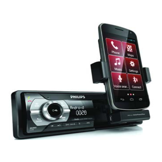
Summary of Contents for Philips CMD305A/05
- Page 1 CMD305A/05 USB/AUX PCB COMPONENT LAYOUT.........17-18 2012-9-6...
- Page 2 CMD305A Dismantlement Method 1. Remove the two screws on the top cover, remove top cover; Then remove the five screws on the heat sink, remove heat sink 2. Remove the six screws on the back cover, remove back cover; Remove the four screws at the left/right side of the unit 3.
-
Page 3: Block Diagram
BLOCK DIAGRAM... -
Page 4: Wiring Diagram
WIRING DIAGRAM... -
Page 5: Circuit Diagram -Main Board
CIRCUIT DIAGRAM -MAIN BOARD... -
Page 7: Circuit Diagram -Servo Board
CIRCUIT DIAGRAM -SERVO BOARD... -
Page 8: Circuit Diagram -Panel Board
CIRCUIT DIAGRAM -PANEL BOARD... - Page 9 CIRCUIT DIAGRAM -DC-DC BOARD...
-
Page 10: Circuit Diagram -Tuner Board
CIRCUIT DIAGRAM -TUNER BOARD XT001 R014 C009 32.768KHz C008 R001 270K C001 L001 C004 Q001 C006 C003 R003 220NH L003 RFGND L002 C002 SK255 2.7UH 220NH IC001 LOUT R002 C005 CTUNE SI474X ROUT RF-GND L006 C017 33UH Q102/Q003 L004 L005 C013 C025 C007... - Page 11 PCB LAYOUT -MAIN BOARD TOP SIDE VIEW...
- Page 12 PCB LAYOUT -MAIN BOARD BOTTOM SIDE VIEW...
- Page 13 PCB LAYOUT -SERVO BOARD TOP SIDE VIEW...
- Page 14 PCB LAYOUT -SERVO BOARD BOTTOM SIDE VIEW...
- Page 15 PCB LAYOUT -PANEL BOARD TOP SIDE VIEW...
- Page 16 PCB LAYOUT -PANEL BOARD BOTTOM SIDE VIEW...
- Page 17 PCB LAYOUT -USB/AUX BOARD TOP SIDE VIEW...
- Page 18 PCB LAYOUT -USB/AUX BOARD BOTTOM SIDE VIEW...
- Page 19 PCB LAYOUT -ANDROID CONNECT BOARD TOP SIDE VIEW...
- Page 20 PCB LAYOUT -ANDROID CONNECT BOARD BOTTOM SIDE VIEW...
- Page 21 PCB LAYOUT -INSPECT BOARD TOP SIDE VIEW...
- Page 22 PCB LAYOUT -DC-DC BOARD TOP SIDE VIEW...
- Page 23 PCB LAYOUT -DC-DC BOARD BOTTOM SIDE VIEW...
- Page 24 PCB LAYOUT -TUNER BOARD TOP SIDE VIEW...
- Page 25 PCB LAYOUT -TUNER BOARD BOTTOM SIDE VIEW...
-
Page 26: Exploded View Drawing
EXPLODED VIEW DRAWING... - Page 27 Product Model CED305A Date 2012-8-16 failure failure cause remark phenomena a To check whether the ISO301 16PIN connector is connected well, to check whether the 15A FUSE in the ISO FILTER BOX is loose. b To check whether the FFC like CON202 CON901( 24PIN socket) which were connected the panel and the unit are inserted in place, whether the lock catch is loose.
- Page 28 J The voltage of the control pin SDA SCL 27 28 of the audio processor IC402 PT7313E should be 3V. a To check whether the AM/FM external antenna is connected well. c To check whether the intensity of radio input signal is too weak. d To check the supply voltage of the 7th pin of the radio board, should be +3V3.


