Table of Contents
Advertisement
Quick Links
SERVICE MANUAL
Ver 1.1 2003. 08
US and foreign patents licensed from Dolby
Laboratories.
• OpenMG, ATRAC, ATRAC3, ATRAC3plus, SonicStage and their logos are trademarks of Sony
Corporation.
• Microsoft, Windows, Windows NT are trademarks or registered trademarks of Microsoft Corporation
in the United States and/or other countries.
• IBM and PC/AT are registered trademarks of International Business Machines Corporation.
• Macintosh is a trademark of Apple Computer, Inc. in the United States and/or other countries.
• Pentium is a trademark or a registered trademark of Intel Corporation.
• Adobe and Acrobat Reader are trademarks of Adobe Systems Incorporated.
• All other trademarks are trademarks of their respective owners.
manual.
MD recorder
Audio playing system
MiniDisc digital audio system
Laser diode properties
Material: GaAlAs
Wavelength: λ = 790 nm
Emission duration: continuous
Laser output: less than 44.6 µW
(This output is the value measured at a distance
of 200 mm from the objective lens surface on
the optical pick-up block with 7 mm aperture.)
Recording and playback time (when
using MDW-80)
Maximum 160 min. in monaural
Maximum 320 min. in LP4 stereo
Revolutions
Approx. 380 rpm to 2,700 rpm
Error correction
ACIRC (Advanced Cross Interleave Reed
Solomon Code)
Sampling frequency
44.1 kHz
Coding
ATRAC (Adaptive TRansform Acoustic
Coding)
ATRAC3 — LP2/LP4
Modulation system
EFM (Eight to Fourteen Modulation)
Number of channels
2 stereo channels
1 monaural channel
Sony Corporation
9-877-460-02
2003H05-1
Personal Audio Company
C 2003.08
Published by Sony Engineering Corporation
TM
and
R
marks are omitted in this
SPECIFICATIONS
Frequency response
20 to 20,000 Hz ± 3 dB
Outputs
i: stereo mini-jack, maximum output level
2 mW + 2 mW, load impedance 16 Ω
(European models)
5 mW + 5 mW, load impedance 16 Ω (other
models)
General
Power requirements
AC Power Adaptor connected at the DC IN 3V
jack:
120 V AC, 60 Hz (Model for Canada)
230 V AC, 50/60 Hz (Model for continental
Europe)
240 V AC, 50 Hz (Model for Australia)
230 V AC, 50 Hz (Model for U.K. and Hong
Kong)
220 V AC, 60 Hz (Model for Korea)
100 – 240 V AC, 50/60 Hz (Other models)
The recorder:
One LR6 (size AA) alkaline battery (not
supplied)
Recommended temperature for
check-in/check-out
+5 °C (+41°F) or higher
PORTABLE MINIDISC RECORDER
AM-NX9
Canadian Model
Australian Model
Model Name Using Similar Mechanism
Mechanism Type
Optical Pick-up Name
Battery operation time
The battery life may be shorter due to operating
conditions and the temperature of the location.
When
playing
1)
When using a new Sony LR6 (size AA)
"STAMINA" alkaline dry battery (produced
in Japan).
2)
Measured in accordance with the JEITA
(Japan Electronics and Information
Technology Industries Association) standard.
Note
The battery life may be shorter than that
specified, depending on the operating
conditions, the temperature of the location, and
varieties of a battery.
AEP Model
UK Model
E Model
MZ-N710
MT-MZN710-177
LCX-5R
Unit: approx.hours (JEITA
2)
)
SP
LP2
LP4
stereo
stereo
stereo
42
48
56
– Continued on next page –
Advertisement
Table of Contents

Related Manuals for Sony AM-NX9


Summary of Contents for Sony AM-NX9
- Page 1 Mechanism Type MT-MZN710-177 Optical Pick-up Name LCX-5R • OpenMG, ATRAC, ATRAC3, ATRAC3plus, SonicStage and their logos are trademarks of Sony Corporation. • Microsoft, Windows, Windows NT are trademarks or registered trademarks of Microsoft Corporation in the United States and/or other countries.
- Page 2 OPERATION. REPLACE THESE COMPONENTS WITH DE FONCTIONNEMENT. NE REMPLACER CES COM- SONY PARTS WHOSE PART NUMBERS APPEAR AS POSANTS QUE PAR DES PIÈCES SONY DONT LES SHOWN IN THIS MANUAL OR IN SUPPLEMENTS PUB- NUMÉROS SONT DONNÉS DANS CE MANUEL OU LISHED BY SONY.
-
Page 3: Table Of Contents
AM-NX9 TABLE OF CONTENTS SERVICING NOTES ..........4 GENERAL ..............5 DISASSEMBLY 3-1. Disassembly Flow ............6 3-2. Cabinet (Lower) .............. 7 3-3. Paper (Case Lower) Ground ........... 7 3-4. MAIN Board ..............8 3-5. Cabinet (Upper) Section ..........8 3-6. -
Page 4: Servicing Notes
AM-NX9 SECTION 1 SERVICING NOTES • The shipment data will be cleared when the NV is reset. There- NOTES ON HANDLING THE OPTICAL PICK-UP fore, change the NV adjusted values following the Change of BLOCK OR BASE UNIT NV Adjusted Values immediately after the NV was reset. (See... -
Page 5: General
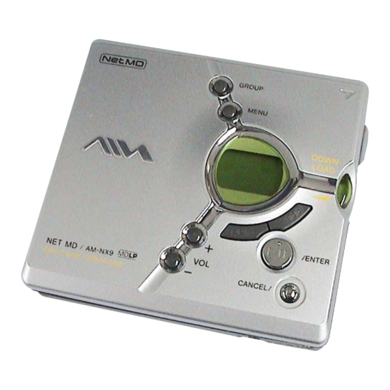
AM-NX9 SECTION 2 This section is extracted from instruction manual. GENERAL Looking at the controls Front of the recorder A GROUP button F xSTOP/CANCEL (stop/cancel) button B MENU button G Display window C VOL +* and – buttons H DOWNLOAD button ∗... -
Page 6: Disassembly
AM-NX9 SECTION 3 DISASSEMBLY • This set can be disassembled in the order shown below. 3-1. DISASSEMBLY FLOW Note 1: The process described in can be performed in any order. Note 2: Without completing the process described in , the next process can not be performed. -
Page 7: Cabinet (Lower)
AM-NX9 Note: Follow the disassembly procedure in the numerical order given. 3-2. CABINET (LOWER) 1 two screws (M1.4) 1 two screws (M1.4) 2 Remove the cabinet (lower) in the direction of the arrow. 3-3. PAPER (CASE LOWER) GROUND 1 paper (case lower) ground... -
Page 8: Main Board
AM-NX9 3-4. MAIN BOARD 1 Remove two solders of the flexible board (over write head). 8 main board 4 four screws (M1.4) 5 battery terminal board (+) 6 battery terminal (–) 3 flexible board (CN872) 7 flexible board (optical pick-up) -
Page 9: Lcd Module
AM-NX9 3-6. LCD MODULE 1 four screws 2 three claws 3 LCD module cabinet (upper) section 3-7. MECHANISM DECK (MT-MZN710-177) 1 two step screws (MD) 3 mechanism deck (MT-MZN710-177) The portion which projected is removed. -
Page 10: Set Chassis Assy
AM-NX9 3-8. SET CHASSIS ASSY 2 two screws (TP 1.7 × 2.5) 4 ground spring (USB) 5 set chassis assy 3 battery case 1 tension spring (lock) 3-9. OP SERVICE ASSY (LCX-5R) 2 gear (SA) 5 screw (M1.4) 1 washer (0.8-2.5) 6 thrust detent spring 3 screw (M1.4) -
Page 11: Holder Assy
AM-NX9 3-10. HOLDER ASSY 4 holder assy 2 Open the holder assy. 3 boss 1 convex portion 3 boss 3-11. DC MOTOR (SLED) (M702) 2 washer (0.8-2.5) 3 gear (SA) 4 two screws (M1.4) 1 Remove six solders of the motor flexible board. -
Page 12: Dc Motor (Over Write Head Up/Down) (M703), Dc Ssm18B Motor (Spindle) (M701)
AM-NX9 3-12. DC MOTOR (OVER WRITE HEAD UP/DOWN) (M703), DC SSM18B MOTOR (SPINDLE) (M701) 1 Remove six solders of the motor flexible board. 2 tapping screw 3 motor cover 7 DC motor (over write head up/down) (M703) Note: Press-fit the gear (HA) up to the position of the DC motor (over write head up/down) (M703) as shown below. -
Page 13: Test Mode
AM-NX9 SECTION 4 TEST MODE Outline Operation in Setting the Test Mode • This set provides the Overall adjustment mode that allows CD • When the test mode becomes active, first the display check mode and MO discs to be automatically adjusted when in the test mode. - Page 14 AM-NX9 Configuration of Test Mode [VOL +] key: 100th place of item number [Major item switching] increase. [Test Mode $Display Check Mode%] [VOL --] key: 100th place of item number decrease. [VOL +] > STOP/CANCEL x Press the > [Manual Mode]...
- Page 15 AM-NX9 5. The display changes a shown below each time the Overall Adjustment Mode [DOWN LOAD] key is pressed. Mode to adjust the servo automatically in all items. Normally, automatic adjustment is executed in this mode at the repair. • Address & Adjusted Value Display For further information, refer to “SECTION 5 ELECTRICAL...
- Page 16 AM-NX9 • Description of Error Indication Codes Problem Indication code Meaning of code Simple display Description No error No error No error Illegal access target Adrs Attempt to access an abnormal address address was specified Servo system error High temperature...
- Page 17 AM-NX9 Sound Skip Check Result Display Mode • Cause of Sound Skip Error This set can display the count of errors that occurred during the Cause of error Description of error recording/playing for checking. Sound error correction error • Setting Method of Sound Skip Check Result Display...
-
Page 18: Electrical Adjustments
2. Use the following tools and measuring instruments. • Test CD disc TDYS-1 R e s e t ! (Part No. : 4-963-646-01) • SONY MO disc available on the market • Digital voltmeter 4. Press the STOP/CANCELx key to quit the manual mode, and •... - Page 19 AM-NX9 • Adjustment Method of VC1_LOW (PB) • Adjustment Method of VC2_LOW (item number: 741) (item number: 743) Set LCD display Set LCD display V C 2 L o V C 1 L 1. Connect a digital voltmeter to the TP1905 (VCOUT) on the...
- Page 20 AM-NX9 • Adjustment Method of REG1 • Adjustment Method of REG3_LOW2 (item number: 745) (item number: 748) Set LCD display Set LCD display R E G 3 L 2 R E G 1 1. Connect a digital voltmeter to the TP1907 (REGO3) on the...
- Page 21 AM-NX9 • Adjustment Method of VREC_LOW (X2 speed) • Adjustment Method of VREC_HIGH (HEAD MOTOR) (item number: 751) (item number: 753) Set LCD display Set LCD display V R E C L V R E C H 1. Connect a digital voltmeter to the TP1620 (VREC) on the 1.
- Page 22 AM-NX9 Adjustment and Connection Location: – MAIN Board (Conductor Side) – BATT – (GND) TP1907 (REGO3) TP1905 (VCOUT) TP1928 TP1909 (VCO1) (REGO1) TP1620 (VREC)
- Page 23 AM-NX9 Power Supply Adjustment Auto Item Feed to the next item. 5. Connect a digital voltmeter to the measuring points on the [VOL +] Note: This mode is available to perform the temperature correction and MAIN board, and adjust the voltage with the power supply adjustment without entering the manual mode.
- Page 24 AM-NX9 Laser Power Check 9. Check that the laser power meter reading is 4.95 ± 0.59 mW. 10. Press the > key, and set the laser MO (X4 speed) write Note: If result of measurement of the laser power does not satisfy the specification, either replace the OP (optical pick-up unit) or check check mode (item number 014).
- Page 25 AM-NX9 • Adjustment Method of CD and MO Overall Adjustment 8. If OK through the MO overall adjustments, press the Mode STOP/CANCEL x key to return to the test mode and termi- 1. Set the test mode (see page 13).
- Page 26 AM-NX9 2. MO overall adjustment items Item No. Description Item No. Description Focus gain adjustment VC,VR power supply H/L selection Tracking gain adjustment R_GRV setting . servo OFF TWPP gain adjustment Low reflection electrical offset adjustment TWPP offset adjustment 1 Laser ON .
- Page 27 AM-NX9 Remuse Clear Perform the Resume clear when all adjustments completed. • Resume Clear Setting Method 1. Select the manual mode of the test mode, and set item number 043 (see page 14). Set LCD display R e s u m e 2.
- Page 28 AM-NX9 Rewriting the Patch Data and NV values at Replacement of Main Board This set requires the patch data in the nonvolatile memory (IC852) to be rewritten using the application, when the MAIN board was replaced. Caution: The application that meets the microcomputer version in this set must be used when rewriting the patch data. Rewriting the patch data using the application not suitable for the microcomputer version could cause the set to malfunction.
- Page 29 AM-NX9 5. Confirm that the model and version indicated on the title bar coincide with the codes displayed in the Device Name block and the Version block in the window. 6. Click the [Write + Read] button. The patch data and NV values writing and the verify processing will be executed automatically.
- Page 30 AM-NX9 MEMO...
-
Page 31: Diagrams
AM-NX9 SECTION 6 DIAGRAMS 6-1. BLOCK DIAGRAM – MAIN Section – OVER WRITE HEAD DRIVE IC601 (1/2) HR601 OVER WRITE OVER HEAD DRIVE OPTICAL PICK-UP BLOCK WRITE PRE DRIVER Q601, 602 (LCX-5R) HEAD (Page 32) OUTA VRECIN2 VRECO H-BRIDGE M703... -
Page 32: Block Diagram - Power Supply Section
AM-NX9 6-2. BLOCK DIAGRAM – POWER SUPPLY Section – POWER CONTROL IC901 (Page 31) SDO0 DATA SDO0 SCK0 SCK0 (Page 31) XWAKE2 XWAKE4 FFCLR FFCLR SLEEP SLEEP D902 XCS PWR IC STRB XRST XRST2 S801 VCIN HALF HALF LOCK SW... -
Page 33: Schematic Diagrams
AM-NX9 Ver 1.1 6-3. NOTE FOR PRINTED WIRING BOARDS AND SCHEMATIC DIAGRAMS • Waveforms 1 IC501 9 (RFO) 5 IC801 2 (OSCO) Note on Printed Wiring Board: Note on Schematic Diagram: • All capacitors are in µF unless otherwise noted. pF: µµF •... -
Page 34: Printed Wiring Board - Main Board (Component Side)
AM-NX9 6-4. PRINTED WIRING BOARD – MAIN Board (Component Side) – :Uses unleaded solder. • Semiconductor Location Ref. No. Location D603 D606 D607 D801 I-10 D802 I-10 D903 D958 S801 D961 (HALF LOCK) IC301 E-10 IC701 Q301 D-10 Q501 Q602... -
Page 35: Printed Wiring Board - Main Board (Conductor Side)
AM-NX9 Ver 1.1 6-5. PRINTED WIRING BOARD – MAIN Board (Conductor Side) – :Uses unleaded solder. • Semiconductor Location Ref. No. Location D171 MAIN BOARD (CONDUCTOR SIDE) D271 D371 D605 D652 M702 D653 (SLED) D654 D901 S806 D902 PROTECT M703... -
Page 36: Schematic Diagram - Main Board (1/4)
AM-NX9 6-6. SCHEMATIC DIAGRAM – MAIN Board (1/4) – • • See page 33 for Waveforms. See page 40 for IC Block Diagrams. (1/4) C513 C517 C524 0.022 0.01 R504 C720 R505 CN501 R511 TRK- C718 TRK- TRK+ TRK+ FCS-... - Page 37 AM-NX9 6-7. SCHEMATIC DIAGRAM – MAIN Board (2/4) – • See page 33 for Waveforms. (2/4) R835 4.7k X802 48MHz R826 R825 2.2k R858 R823 R834 FS256 C819 FB802 R828 4.7k R837 R839 R821 R822 R824 R843 220k 470k C841...
-
Page 38: Schematic Diagram - Main Board (3/4)
AM-NX9 6-8. SCHEMATIC DIAGRAM – MAIN Board (3/4) – • • See page 33 for Waveform. See page 40 for IC Block Diagrams. (Page 36) (3/4) TP1620 C631 (V_REC) C630 Q604 C615 C617 MCH6616-TL-E OVER WRITE HEAD DRIVE R612 R613... -
Page 39: Schematic Diagram - Main Board (4/4)
AM-NX9 Ver 1.1 6-9. SCHEMATIC DIAGRAM – MAIN Board (4/4) – • • See page 33 for Waveform. See page 40 for IC Block Diagrams. (Page 37) (4/4) C306 C305 6.3V R302 Q301 4.7k 2SC4738F-Y/GR R301 VOLTAGE 2.2k SWITCHING VREF_IN C304 6.3V... - Page 40 AM-NX9 • IC Block Diagrams IC301 TA2131FL (EL) IC601 XPC18A22AEPR2 BEEP V REF VREF LPF1 VC2 VG MT TC OUTPUT SW CHARGE CHARGE PUMP 2 PUMP 1 VCC1 OUTPUT SW VC VG DC IN BST NF1 BST1 CHARGE MONITOR HI-BRIDGE...
- Page 41 AM-NX9 IC701 SC111258EPR2 42 41 35 34 31 30 29 PWM2 3PHASE CONTROL 3PHASE H-BRIDGE H-BRIDGE PRE DRIVER PRE DRIVER CONTROL VC LOW VOLTAGE DETECTOR COM2 CPUI2 – CPUO2 CPVO2 – CPVI2 CPWO2 – CPWI2 BIAS GND2 VC VG GND1 –...
- Page 42 AM-NX9 IC901 SC901580EPR2 (HP AMP) AMP1 CONTROL BANDGAP FFCLR1 48 VREF REFERENCE XWK4 47 REGC3 REF1 XWK3 46 REGC2 REF2 REF3 XWK2 45 REGC1 REF4 REF5 XWK1 44 REGI1 SERIES PASS REGULATOR1 REF3 VRMC 43 REGO1 FFCLR 42 VC2 SERIES PASS...
-
Page 43: Ic Pin Function Description
AM-NX9 6-10. IC PIN FUNCTION DESCRIPTION • IC501 SN761058AZQLR (RF AMP, FOCUS/TRACKING ERROR AMP) Pin No. Pin Name Description I-V converted RF signal (IX) input from the optical pickup detector 2, 3 PS, EQ — Connected to the external capacitor for the RF and EQ AGND —... - Page 44 AM-NX9 Pin No. Pin Name Description PEAK Peak hold signal output of the light amount signal (RF/ABCD) to the system controller Signal (D) input from the optical pickup detector Signal (A) input from the optical pickup detector Signal (B) input from the optical pickup detector...
- Page 45 AM-NX9 • IC801 CXD2680-207GA (SYSTEM CONTROLLER, DIGITAL SIGNAL PROCESSOR, 16M BIT D-RAM) Pin No. Description Pin Name OSCI Resonator connection terminal for the system clock (22.5792MHz) OSCO Resonator connection terminal for the system clock (22.5792MHz) VREFL Reference voltage terminal connected to the capacitor (for the built-in D/A converter L-CH)
- Page 46 AM-NX9 Pin No. Pin Name Description SLCV Sled motor drive comparison signal input (V) from the motor driver SLCW Sled motor drive comparison signal input (W) from the motor driver SRDR Sled motor drive control signal output (U) to the motor driver Digital audio signal input (fixed at “L”...
- Page 47 AM-NX9 Pin No. Pin Name Description Serial data input from the nonvolatile memory Serial data output to the nonvolatile memory, liquid crystal display module and power control SCK0 Serial clock output to the nonvolatile memory, liquid crystal display module and power control Rechargeable battery detection switch input terminal “L”: rechargeable battery in detect...
- Page 48 AM-NX9 Pin No. Pin Name Description VREC_PWM PWM signal output for the power supply voltage control to the REC driver VL_PWM PWM signal output for the laser power supply voltage control to the power control Not used NJM_XMUTE Muting control signal terminal (NJM type made by JRC) Not used...
- Page 49 AM-NX9 Pin No. Pin Name Description SET_CODE2 Input terminal for the set (open in this set) SET_CODE3 Input terminal for the set (open in this set) 195, 196 Not used VBUS5V_DET Not used LG_DCR_CTL Not used MUTE Analog muting control signal output to the headphone amplifier “H”: muting ON Not used...
- Page 50 AM-NX9 Pin No. Pin Name Description IFVDD4 — Power supply terminal (for the microcomputer I/F block) IFVSS4 — Ground terminal (for the microcomputer I/F block) AVDD — Power supply terminal (for the microcomputer analog) AVSS — Ground terminal (for the microcomputer analog) VDIOSC —...
-
Page 51: Exploded Views
AM-NX9 Ver 1.1 SECTION 7 EXPLODED VIEWS NOTE: • -XX and -X mean standardized parts, so they • Items marked “*” are not stocked since they The components identified by mark may have some difference from the original are seldom required for routine service. Some 0 or dotted line with mark 0 are one. -
Page 52: Chassis Section
AM-NX9 7-2. CHASSIS SECTION mechanism deck section-1 (MT-MZN710-177) not supplied not supplied main board section Ref. No. Part No. Description Remark Ref. No. Part No. Description Remark 3-237-072-02 SCREW (MD), STEP 3-250-692-01 SPRING (USB), GROUND 3-238-876-07 SCREW (M1.4), TOOTHED LOCK 3-318-382-91 SCREW (1.7X2.5), TAPPING... -
Page 53: Main Board Section
AM-NX9 Ver 1.1 7-3. MAIN BOARD SECTION not supplied main board Ref. No. Part No. Description Remark Ref. No. Part No. Description Remark 3-246-247-03 CASE, BATTERY * 104 X-3383-984-1 MAIN BOARD, COMPLETE (AEP, UK, EE) 3-237-073-01 TERMINAL BOARD (+), BATTERY... -
Page 54: Mechanism Deck Section-1 (Mt-Mzn710-177)
AM-NX9 7-4. MECHANISM DECK SECTION-1 (MT-MZN710-177) mechanism deck section-2 (MT-MZN710-177) not supplied The components identified by Les composants identifiés par une mark 0 or dotted line with marque 0 sont critiques pour la mark 0 are critical for safety. sécurité. -
Page 55: Mechanism Deck Section-2 (Mt-Mzn710-177)
AM-NX9 7-5. MECHANISM DECK SECTION-2 (MT-MZN710-177) M702 M703 M701 Ref. No. Part No. Description Remark Ref. No. Part No. Description Remark 3-225-278-12 SCREW, TAPPING 3-225-996-07 SCREW (M1.4) (EG), PRECISION PAN 3-235-838-02 COVER, MOTOR 3-235-839-02 LEVER (RACK) 3-235-836-01 GEAR (HB) 3-338-645-31 WASHER (0.8-2.5) -
Page 56: Electrical Parts List
AM-NX9 Ver 1.1 SECTION 8 MAIN ELECTRICAL PARTS LIST NOTE: The components identified by • Due to standardization, replacements in the • Items marked “*” are not stocked since they mark 0 or dotted line with mark 0 are critical for safety. - Page 57 AM-NX9 Ver 1.1 MAIN Ref. No. Part No. Description Remark Ref. No. Part No. Description Remark C932 1-125-838-11 CERAMIC CHIP 2.2uF 6.3V C718 1-107-820-11 CERAMIC CHIP 0.1uF C933 1-164-943-11 CERAMIC CHIP 0.01uF C719 1-107-820-11 CERAMIC CHIP 0.1uF C957 1-107-820-11 CERAMIC CHIP 0.1uF...
- Page 58 AM-NX9 Ver 1.1 MAIN Ref. No. Part No. Description Remark Ref. No. Part No. Description Remark FB901 1-400-050-11 FERRITE R110 1-218-937-11 RES-CHIP 1/16W (AEP, UK, EE) < IC > R175 1-208-635-11 RES-CHIP 1/16W R176 1-218-961-11 RES-CHIP 4.7K 1/16W IC301 8-759-598-15 IC TA2131FL (EL)
- Page 59 AM-NX9 Ver 1.1 MAIN Ref. No. Part No. Description Remark Ref. No. Part No. Description Remark R706 1-218-965-11 RES-CHIP 1/16W R905 1-208-707-11 METAL CHIP 0.5% 1/16W R803 1-208-635-11 RES-CHIP 1/16W R907 1-218-985-11 RES-CHIP 470K 1/16W R804 1-208-635-11 RES-CHIP 1/16W R805...
- Page 60 AM-NX9 Ver 1.1 Ref. No. Part No. Description Remark Ref. No. Part No. Description Remark ACCESSORIES ************ 1-477-563-41 ADAPTOR, AC (AC-ES305K) (KR) 1-477-565-41 ADAPTOR, AC (AC-ES305K) (AEP, EE) 1-477-566-41 ADAPTOR, AC (AC-ES305K) (UK, HK) 1-477-568-31 ADAPTOR, AC (AC-ES305K) (AUS) 1-477-570-31 ADAPTOR, AC (AC-ES305K) (E)
- Page 61 AM-NX9 MEMO...
- Page 62 AM-NX9 REVISION HISTORY Clicking the version allows you to jump to the revised page. Also, clicking the version at the upper right on the revised page allows you to jump to the next revised page. Ver. Date Description of Revision 2003.06...