Table of Contents
Advertisement
Quick Links
Advertisement
Table of Contents

Related Manuals for Asus AAEON PICO-APL4


Summary of Contents for Asus AAEON PICO-APL4
- Page 1 PICO-APL4 PICO-ITX Board User’s Manual 7 Last Updated: May 7, 2021...
- Page 2 Copyright Notice This document is copyrighted, 2021. All rights are reserved. The original manufacturer reserves the right to make improvements to the products described in this manual at any time without notice. No part of this manual may be reproduced, copied, translated, or transmitted in any form or by any means without the prior written permission of the original manufacturer.
- Page 3 Acknowledgement All other product name or trademarks are properties of their respective owners. Microsoft Windows® is a registered trademark of Microsoft Corp. ⚫ Intel®, Pentium® and Celeron® are registered trademarks of Intel Corp. ⚫ Intel Atom™ is a trademark of Intel Corp. ⚫...
- Page 4 Packing List Before setting up your product, please make sure the following items have been shipped: Item Quantity PICO-APL4 If any of these items are missing or damaged, please contact your distributor or sales representative immediately. Preface...
- Page 5 About this Document This User’s Manual contains all the essential information, such as detailed descriptions and explanations on the product’s hardware and software features (if any), its specifications, dimensions, jumper/connector settings/definitions, and driver installation instructions (if any), to facilitate users in setting up their product. Users may refer to the product page at AAEON.com for the latest version of this document.
- Page 6 Safety Precautions Please read the following safety instructions carefully. It is advised that you keep this manual for future references All cautions and warnings on the device should be noted. Make sure the power source matches the power rating of the device. Position the power cord so that people cannot step on it.
- Page 7 If any of the following situations arises, please the contact our service personnel: Damaged power cord or plug Liquid intrusion to the device iii. Exposure to moisture Device is not working as expected or in a manner as described in this manual The device is dropped or damaged Any obvious signs of damage displayed on the device...
- Page 8 FCC Statement This device complies with Part 15 FCC Rules. Operation is subject to the following two conditions: (1) this device may not cause harmful interference, and (2) this device must accept any interference received including interference that may cause undesired operation.
- Page 9 China RoHS Requirements (CN) 产品中有毒有害物质或元素名称及含量 AAEON Main Board/ Daughter Board/ Backplane 有毒有害物质或元素 部件名称 铅 汞 镉 六价铬 多溴联苯 多溴二苯醚 (Pb) (Hg) (Cd) (Cr(VI)) (PBB) (PBDE) 印刷电路板 ○ ○ ○ ○ ○ ○ 及其电子组件 外部信号 ○ ○ ○ ○ ○ ○ 连接器及线材...
- Page 10 China RoHS Requirement (EN) Poisonous or Hazardous Substances or Elements in Products AAEON Main Board/ Daughter Board/ Backplane Poisonous or Hazardous Substances or Elements Hexavalent Polybrominated Polybrominated Component Lead Mercury Cadmium Chromium Biphenyls Diphenyl Ethers (Pb) (Hg) (Cd) (Cr(VI)) (PBB) (PBDE) PCB &...
-
Page 11: Table Of Contents
Table of Contents Chapter 1 - Product Specifications..................1 Specifications ......................2 Chapter 2 – Hardware Information ..................5 Dimensions ....................... 6 Jumpers and Connectors ..................9 List of Jumpers ......................11 2.3.1 Auto Power Button Enable/Disable Selection (JP1) ......11 2.3.2 Clear CMOS Jumper (JP2) .............. - Page 12 2.4.18 Embedded DisplayPort (Optional) (CN19) ........32 2.4.19 USB 2.0 Port 2 (CN20) ................34 2.4.20 USB 2.0 Port 1 (CN21) ................34 2.4.21 LPC Port (CN22) ..................35 Electrical Specifications for I/O Ports ..............36 Function Block ......................37 Assembly Options ....................
- Page 13 3.6.1 Secure Boot ..................... 61 3.6.1.1 Key Management ..............62 Setup Submenu: Boot ..................64 3.7.1 BBS Priorities................... 65 Setup Submenu: Save & Exit ................66 Chapter 4 – Drivers Installation .................... 67 Driver Download/Installation ................68 Appendix A - I/O Information ....................70 I/O Address Map ....................
-
Page 14: Chapter 1 - Product Specifications
Chapter 1 Chapter 1 - Product Specifications... -
Page 15: Specifications
Specifications System Form Factor PICO-ITX Intel® Pentium® N4200 (4-core, 1.1 GHz, up to 2.5 GHz, TDP 6W) Intel® Celeron® N3350 (2-core, 1.1 GHz, up to 2.4 GHz, TDP 6W) Intel® Atom™ x7-Series (4-core 1.6GHz, up to 2.00 GHz, TDP 12W) CPU Frequency Up to 2.4GHz Chipset... - Page 16 System Operating Temperature 32°F ~ 140°F (0°C ~ 60°C) Storage Temperature -40°F ~ 176°F (-40°C ~ 80°C) Operating Humidity 0% ~ 90% relative humidity, non-condensing MTBF (Hours) 191,895 Certification CE, FCC Display Chipset Intel SoC Resolution HDMI 1.4b: 3840 x 2160, 30Hz Internal eDP 1.4: 3840 x 2160, 60Hz (Optional) DDI (Optional from BIO) LCD Interface...
- Page 17 Expansion Slot M.2 2230 x 1 (E-Key) BIO x 1 (optional) Smbus — — Touch — Chapter 1 – Product Specifications...
-
Page 18: Chapter 2 - Hardware Information
Chapter 2 Chapter 2 – Hardware Information... -
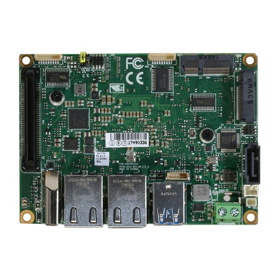
Page 19: Dimensions
Dimensions Component Side Component Side Chapter 2 – Hardware Information... - Page 20 Solder Side Solder Side Chapter 2 – Hardware Information...
- Page 21 Rear I/O Configuration Phoenix DC Jack Chapter 2 – Hardware Information...
-
Page 22: Jumpers And Connectors
Jumpers and Connectors Component Side Component Side Chapter 2 – Hardware Information... - Page 23 Solder Side Solder Side Chapter 2 – Hardware Information...
-
Page 24: List Of Jumpers
List of Jumpers Please refer to the table below for all of the board’s jumpers that you can configure for your application Label Function Auto Power Button Enable/Disable Selection Clear CMOS Jumper 2.3.1 Auto Power Button Enable/Disable Selection (JP1) 1 2 3 Enable/AT (Default) Disable/ATX Note: When disabled, the power button of CN3 (1-2) is used to power on the system... -
Page 25: List Of Connectors
List of Connectors Please refer to the table below for all of the board’s connectors that you can configure for your application Label Function COM Port 2 COM Port 1 Front Panel Connector M.2 Key-E Slot (2230) M.2 Key-B Slot (2280) BIO Port (Optional) Digital I/O SATA Port... -
Page 26: Com Port 2 (Cn1)
2.4.1 COM Port 2 (CN1) RS232 Pin Name Signal Type Signal Level DCD2 DSR2 RTS2 ±5V ±5V CTS2 DTR2 ±5V RI2/+5V/+12V +5V/+12V Chapter 2 – Hardware Information... - Page 27 RS485 Pin Name Signal Type Signal Level RS485_ D2- ±5V RS485_D2+ ±5V NC/+5V/+12V +5V/+12V RS422 Pin Name Signal Type Signal Level RS422_TX2- ±5V RS422_TX2+ ±5V RS422_RX2+ RS422_RX2- NC/+5V/+12V +5V/+12V Note: COM2 RS-232/422/485 can be set by BIOS setting. Default is RS-232. Note: Pin 8 function can be changed by BOM.
-
Page 28: Com Port 1 (Cn2)
2.4.2 COM Port 1 (CN2) RS232 Pin Name Signal Type Signal Level DCD1 DSR1 RTS1 ±9V ±9V CTS1 DTR1 ±9V Chapter 2 – Hardware Information... -
Page 29: Front Panel Connector (Cn3)
2.4.3 Front Panel Connector (CN3) Pin Name Pin Name PWR_BTN- PWR_BTN+ HDD_LED- HDD_LED+ SPEAKER- SPEAKER+ PWR_LED- PWR_LED+ H/W RESET- H/W RESET+ 2.4.4 M.2 Key-E Slot (2230) (CN4) Pin Name Signal Type Signal Level +3.3VSB +3.3V USB_D+ DIFF +3.3VSB +3.3V USB_D- DIFF Chapter 2 –... - Page 30 Pin Name Signal Type Signal Level PCIE_TX+ DIFF PCIE_TX- DIFF PCIE_RX+ DIFF PCIE_RX- DIFF Chapter 2 – Hardware Information...
- Page 31 Pin Name Signal Type Signal Level PCIE_REF_CLK+ DIFF PCIE_REF_CLK- DIFF PCIE_RST# +3.3V PCIE_CLK_REQ# +3.3V W_DISABLE2# +3.3V PCIE_WAKE# +3.3V W_DISABLE1# +3.3V Chapter 2 – Hardware Information...
-
Page 32: Key-B Slot (2280) (Cn5)
Pin Name Signal Type Signal Level +3.3VSB +3.3V +3.3VSB +3.3V 2.4.5 M.2 Key-B Slot (2280) (CN5) Pin Name Signal Type Signal Level +3.3V +3.3V +3.3V +3.3V USB_D+ DIFF USB_D- DIFF SSD_DAS# +3.3V Chapter 2 – Hardware Information... - Page 33 Pin Name Signal Type Signal Level DEVSLP +1.8V SATA_RX+ DIFF SATA_RX- DIFF SATA_TX- DIFF SATA_TX+ DIFF Chapter 2 – Hardware Information...
- Page 34 Pin Name Signal Type Signal Level +3.3V +3.3V +3.3V +3.3V +3.3V +3.3V Chapter 2 – Hardware Information...
-
Page 35: Bio Port (Optional) (Cn6)
2.4.6 BIO Port (Optional) (CN6) Pin Name Signal Type Signal Level +12VSB +12V PCIE_TXN0 DIFF PCIE_RXN0 DIFF PCIE_TXP0 DIFF PCIE_RXP0 DIFF PCIE_TXN1 DIFF PCIE_RXN1 DIFF PCIE_TXP1 DIFF PCIE_RXP1 DIFF Chapter 2 – Hardware Information... - Page 36 Pin Name Signal Type Signal Level PS_ON# DDI_DDCCLK +3.3V DDI_DDCDATA +3.3V +5VSB +5VSB +5VSB +5VSB PCIE_REF_CLK0 DIFF RESET# PCIE_REF_CLK0# DIFF DDI_TX1N DIFF DDI_TX0N DIFF DDI_TX1P DIFF DDI_TX0P DIFF DDI_TX3N DIFF DDI_TX2N DIFF DDI_TX3P DIFF DDI_TX2P DIFF Chapter 2 – Hardware Information...
- Page 37 Pin Name Signal Type Signal Level DDI_HPD DDI_AUXN DIFF DDI0_AUXP DIFF USB3_TX_N DIFF USB3_TX_P DIFF USB_D0- DIFF USB_D0+ DIFF USB3_RX_N DIFF USB3_RX_P DIFF SMB_CLK +3.3V SMB_DATA +3.3V WAKE# +3.3V USB_OC# +3.3V USB_OC# +3.3V LPC_AD0 +3.3V Chapter 2 – Hardware Information...
-
Page 38: Digital I/O (Cn7)
Pin Name Signal Type Signal Level LPC_FRAME# +3.3V LPC_AD1 +3.3V SERIRQ +3.3V LPC_AD2 +3.3V LPC_AD3 +3.3V BIO_PWOK +3.3V LPC_CLK +3.3V 2.4.7 Digital I/O (CN7) Pin Name Signal Type Signal Level DIO0 DIO1 Chapter 2 – Hardware Information... -
Page 39: Sata Port (Cn8)
Pin Name Signal Type Signal Level DIO2 DIO3 2.4.8 SATA Port (CN8) Pin Name Signal Type Signal Level SATA_TX+ DIFF SATA_TX- DIFF SATA_RX- DIFF SATA_RX+ DIFF Chapter 2 – Hardware Information... -
Page 40: Spi Flash Programming Port (Cn9)
2.4.9 SPI Flash Programming Port (CN9) Pin Name Signal Type Signal Level SPI_MISO SPI_CLK +3.3VSB +3.3V SPI_MOSI SPI_CS 2.4.10 +5V Output for SATA HDD (CN12) Pin Name Signal Type Signal Level Chapter 2 – Hardware Information... -
Page 41: Hdmi Port (Cn11)
2.4.11 HDMI Port (CN11) Pin Name Signal Type Signal level TMDS_DAT2+ DIFF TMDS_DAT2- DIFF TMDS_DAT1+ DIFF TMDS_DAT1- DIFF TMDS_DAT0+ DIFF TMDS_DAT0- DIFF TMDS_CLK+ DIFF TMDS_CLK- DIFF DDC_CLK DDC_DATA HPLG_DETECT Chapter 2 – Hardware Information... -
Page 42: Battery (Cn12)
2.4.12 Battery (CN12) Pin Name Signal Type Signal Level +3.3V 3.3V 2.4.13 LAN (RJ-45) Port1 (CN13) Pin Name Signal Type Signal level MDI0+ DIFF MDI0- DIFF MDI1+ DIFF MDI2+ DIFF MDI2- DIFF MDI1- DIFF MDI3+ DIFF MDI3- DIFF Chapter 2 – Hardware Information... -
Page 43: Lan (Rj-45) Port2 (Cn14)
2.4.14 LAN (RJ-45) Port2 (CN14) Pin Name Signal Type Signal Level MDI0+ DIFF MDI0- DIFF MDI1+ DIFF MDI2+ DIFF MDI2- DIFF MDI1- DIFF MDI3+ DIFF MDI3- DIFF Chapter 2 – Hardware Information... -
Page 44: Usb 3.0 Ports 0 And 1 (Cn15)
2.4.15 USB 3.0 Ports 0 and 1 (CN15) Pin Name Signal Type Signal Level +5VSB USB0_D- DIFF USB0_D+ DIFF USB0_SSRX− DIFF USB0_SSRX+ DIFF USB0_SSTX− DIFF USB0_SSTX+ DIFF +5VSB USB1_D- DIFF USB1_D+ DIFF USB1_SSRX− DIFF USB1_SSRX+ DIFF USB1_SSTX− DIFF USB1_SSTX+ DIFF Chapter 2 –... -
Page 45: External Power Input (Cn17)
2.4.16 External Power Input (CN17) Pin Name Signal Type Signal Level +VIN +12V 2.4.17 +12V DC Power Jack (Optional) (CN18) Pin Name Signal Type Signal Level +12V +12V 2.4.18 Embedded DisplayPort (Optional) (CN19) Pin Name Signal Type Signal Level VCC_PWR 3.3V VCC_PWR 3.3V... - Page 46 Pin Name Signal Type Signal Level EDP_TX1_N DIFF EDP_TX1_P DIFF EDP_TX0_N DIFF EDP_TX0_P DIFF EDP_TX3_N DIFF EDP_TX3_P DIFF EDP_AUXN DIFF EDP_AUXP DIFF EDP_BKLTNESS +3.3V EDP_BKLTEN +3.3V EDP_HPD +12V +12V +12V +12V +12V +12V +12V +12V Chapter 2 – Hardware Information...
-
Page 47: Usb 2.0 Port 2 (Cn20)
2.4.19 USB 2.0 Port 2 (CN20) Pin Name Signal Type Signal Level +5VSB USB_D- DIFF USB_D+ DIFF 2.4.20 USB 2.0 Port 1 (CN21) Pin Name Signal Type Signal Level +5VSB USB_D- DIFF USB_D+ DIFF Chapter 2 – Hardware Information... -
Page 48: Lpc Port (Cn22)
2.4.21 LPC Port (CN22) Pin Name Signal Type Signal Level LAD0 +3.3V LAD1 +3.3V LAD2 +3.3V LAD3 +3.3V +3.3V +3.3V LFRAME# LRESET# +3.3V LCLK SMB_DATA/I2C_SDA +3.3V SMB_CLK/I2C_SCL +3.3V SMB_ALERT/INT_SERIRQ I/O +3.3V Note: I2C/SMBus (pins 10, 11, 12) can be set by Bios Option Menu (BOM) R406/R403/R414: I2C (default) R405/R408/R411: SMBus Chapter 2 –... -
Page 49: Electrical Specifications For I/O Ports
Electrical Specifications for I/O Ports Reference Signal Level Rate Output COM Port 2 +5V/+12V +5V/0.5A or +12V/0.5A M.2 Key-E Slot (2230) +3.3VSB +3.3V/2A M.2 Key-B Slot (2280) +3.3V +3.3V/2.5A Digital IO Port +5V/1A +5V Output for SATA HDD CN10 +5V/1A USB Ports 0 and 1 CN15 +5VSB... -
Page 50: Function Block
Function Block Chapter 2 – Hardware Information... -
Page 51: Assembly Options
Assembly Options 2.7.1 PICO-APL4-HSK01 AAEON provides a heat spreader and a heatsink with both studs and screws included as options. AAEON suggests using both for assembly. Note: For best performance and reliability, AAEON advises enabling a power limit in BIOS setup when using a passive cooling solution. Chapter 2 –... -
Page 52: Pico-Apl4-Hsp01
2.7.2 PICO-APL4-HSP01 If installing the PICO-APL4 onto a chassis with only the heat spreader provided by AAEON, make sure to apply thermal grease between the heat spreader and chassis. Chapter 2 – Hardware Information... -
Page 53: Pico-Apl4-Fan01
2.7.3 PICO-APL4-FAN01 Note: The active cooling solution can be operated via +5V USB power from CN20 or CN21 without fan speed control. Chapter 2 – Hardware Information... -
Page 54: Chapter 3 - Ami Bios Setup
Chapter 3 Chapter 3 - AMI BIOS Setup... -
Page 55: System Test And Initialization
System Test and Initialization These routines test and initialize board hardware. If the routines encounter an error during the tests, you will either hear a few short beeps or see an error message on the screen. There are two kinds of errors: fatal and non-fatal. The system can usually continue the boot up sequence with non-fatal errors. -
Page 56: Ami Bios Setup
AMI BIOS Setup AMI BIOS ROM has a built-in Setup program that allows users to modify the basic system configuration. This type of information is stored in battery-backed CMOS RAM and BIOS NVRAM so that it retains the Setup information when the power is turned off. Entering Setup Power on the computer and press <Del>or <ESC>... -
Page 57: Setup Submenu: Main
Setup Submenu: Main Chapter 3 – AMI BIOS Setup... -
Page 58: Setup Submenu: Advanced
Setup Submenu: Advanced Chapter 3 – AMI BIOS Setup... -
Page 59: Trusted Computing
3.4.1 Trusted Computing Options Summary Security Device Support Disable Enable Optimal Default, Failsafe Default Enables or Disables BIOS support for security device. O.S. will not show Security Device. TCG EFI protocol and INT1A interface will not be available. SHA-1 PCR Bank Disable Enable Optimal Default, Failsafe Default... - Page 60 Options Summary Storage Hierarchy Disabled Enabled Optimal Default, Failsafe Default Enable or Disable Storage Hierarchy Endorsement Hierarchy Disabled Enabled Optimal Default, Failsafe Default Enable or Disable Endorsement Hierarchy TPM2.0 UEFI Spec Version TCG_1_2 TCG_2 Optimal Default, Failsafe Default Select the TCG2 Spec Version Support, TCG_1_2: the Compatible mode for Win8/Win10 TCG_2: Support new TCG2 protocol and event format for Win10 or later Physical Presence Spec...
-
Page 61: Cpu Configuration
3.4.2 CPU Configuration Options Summary C-States Disabled Enabled Optimal Default, Failsafe Default Enable/Disable C States. EIST™ Disabled Enabled Optimal Default, Failsafe Default Enable/Disable Intel SpeedStep. Turbo Mode Disabled Enabled Optimal Default, Failsafe Default Turbo Mode Intel Virtualization Disabled Technology Enabled Optimal Default, Failsafe Default When enabled, a VMM can utilize the additional hardware capabilities provided by Vanderpool Technology. - Page 62 Options Summary Power Limit 1 Enable Disabled Optimal Default, Failsafe Default Enabled Enable/Disable Power Limit 1 Chapter 3 – AMI BIOS Setup...
-
Page 63: Sata Configuration
3.4.3 SATA Configuration Options Summary SATA GEN SPEED AUTO Optimal Default, Failsafe Default GEN1 GEN2 GEN3 SATA GEN SPEED SELECTION Port0 / M.2 port Disabled Enabled Optimal Default, Failsafe Default Enable/Disable SATA port SATA Port 0 Hot Plug Disabled Optimal Default, Failsafe Default Capability Enabled Enable/Disable SATA port hot plug... -
Page 64: Hardware Monitor
3.4.4 Hardware Monitor Chapter 3 – AMI BIOS Setup... -
Page 65: Sio Configuration
3.4.5 SIO Configuration Chapter 3 – AMI BIOS Setup... -
Page 66: Serial Port 1 Configuration
3.4.5.1 Serial Port 1 Configuration Options Summary Use This Device Disable Enable Optimal Default, Failsafe Default Enable or Disable this Logical Device. Possible: Use Automatic Settings Optimal Default, Failsafe Default IO=3F8h; IRQ=4 IO=2F8h; IRQ=3 Allows user to change Device's Resource settings. New settings will be reflected on This Setup Page after System restarts. -
Page 67: Serial Port 2 Configuration
3.4.5.2 Serial Port 2 Configuration Options Summary Use This Device Disable Enable Optimal Default, Failsafe Default Enable or Disable this Logical Device. Possible: Use Automatic Settings Optimal Default, Failsafe Default IO=2F8h; IRQ=3 IO=3F8h; IRQ=4 Allows user to change Device's Resource settings. New settings will be reflected on This Setup Page after System restarts. -
Page 68: Digital Io Port Configuration
3.4.5 Digital IO Port Configuration Options Summary DIO Port* Output Input Set DIO as Input or Output Output Level High Optimal Default, Failsafe Default Set output level when DIO pin is output Chapter 3 – AMI BIOS Setup... -
Page 69: Power Management
3.4.6 Power Management Options Summary Power Mode ATX Type Optimal Default, Failsafe Default AT Type Select system power mode Restore AC Power Loss Last State Optimal Default, Failsafe Default Always On Always Off Determine the system turn on or off after AC resume from G3 to S5 state RTC wake system from S5 Disable Optimal Default, Failsafe Default... -
Page 70: Setup Submenu: Chipset
Setup Submenu: Chipset Chapter 3 – AMI BIOS Setup... -
Page 71: North Bridge
3.5.1 North Bridge Chapter 3 – AMI BIOS Setup... -
Page 72: South Bridge
3.5.2 South Bridge Options Summary M.2 PCI Express Root Port Disable Enable Optimal Default, Failsafe Default Auto Control the PCI Express Root Port. AUTO: To disable unused root port automatically for the most optimum power savings. Enable: Enable PCIe root port Disable: Disable PCIe root port M.2 PCIe Speed Auto... -
Page 73: Setup Submenu: Security
Setup Submenu: Security Change User/Administrator Password You can set an Administrator Password or User Password. An Administrator Password must be set before you can set a User Password. The password will be required during boot up, or when the user enters the Setup utility. A User Password does not provide access to many of the features in the Setup utility. -
Page 74: Secure Boot
3.6.1 Secure Boot Options Summary Secure Boot Disabled Optimal Default, Failsafe Default Enabled Secure Boot feature is Active if Secure Boot is Enabled, Platform Key(PK) is enrolled and the System is in User mode. The mode change requires platform reset Secure Boot Mode Custom Optimal Default, Failsafe Default... -
Page 75: Key Management
3.6.1.1 Key Management Options Summary Factory Key Provision Disabled Optimal Default, Failsafe Default Enabled Secure Boot feature is Active if Secure Boot is Enabled, Platform Key(PK) is enrolled and the System is in User mode. The mode change requires platform reset Restore Factory Keys Force System to User Mode. - Page 76 Options Summary Restore DB defaults Restore DB variable to factory defaults Platform Key (PK) Details Export Update Delete Key Exchange Keys Details Export Update Append Delete Authorized Signatures Details Export Update Append Delete Forbidden Signatures Details Export Update Append Delete Authorized Time Stamps Update Append...
-
Page 77: Setup Submenu: Boot
Setup Submenu: Boot Options Summary Quiet Boot Disabled Enabled Optimal Default, Failsafe Default Enables or Disables showing boot logo. Monitor Mwait Disable Enabled Auto Optimal Default, Failsafe Default Enable/Disable Monitor Mwait. To install Linux OS, please set this item to disable. Ipv4 PXE Support Disabled Optimal Default, Failsafe Default... -
Page 78: Bbs Priorities
3.7.1 BBS Priorities Chapter 3 – AMI BIOS Setup... -
Page 79: Setup Submenu: Save & Exit
Setup Submenu: Save & Exit Chapter 3 – AMI BIOS Setup... -
Page 80: Chapter 4 - Drivers Installation
Chapter 4 Chapter 4 – Drivers Installation... -
Page 81: Driver Download/Installation
Driver Download/Installation Drivers for the PICO-APL4 can be downloaded from the product page on the AAEON website by following this link: https://www.aaeon.com/en/p/pico-itx-boards-pico-apl4#downloads Download the driver(s) you need and follow the steps below to install them. Step 1 – Install Chipset Driver Open the STEP1 - CHIPSET folder and open the SetupChipset.exe file Follow the instructions Drivers will be installed automatically... - Page 82 Step 4 – Install Audio Driver Open the STEP4 - AUDIO folder and open the 0006-64bit_Win7_Win8_Win81_Win10_R279.exe file Follow the instructions Driver will be installed automatically Step 5 – Install TXE Driver Open the STEP5 - TXE folder and open the SetupTXE.exe file Follow the instructions Driver will be installed automatically Chapter 4 –...
-
Page 83: Appendix A - I/O Information
Appendix A Appendix A - I/O Information... -
Page 84: I/O Address Map
I/O Address Map Appendix A – I/O Information... -
Page 85: A.2 Memory Address Map
A.2 Memory Address Map Appendix A – I/O Information... -
Page 86: A.3 Irq Mapping Chart
A.3 IRQ Mapping Chart Appendix A – I/O Information... - Page 87 Appendix A – I/O Information...
- Page 88 Appendix A – I/O Information...
-
Page 89: Appendix B - Mating Connectors
Appendix B Appendix B – Mating Connectors... -
Page 90: List Of Mating Connectors And Cables
List of Mating Connectors and Cables The table notes mating connectors and available cables. Mating Connector Connector Available Function Cable P/N Label Cable Vendor Model no COM Port #2 Serial Port SHR-09V-S-B 1701090122 Connector Cable COM Port #1 Serial Port SHR-09V-S-B 1701090122 Connector...