Table of Contents
Advertisement
Quick Links
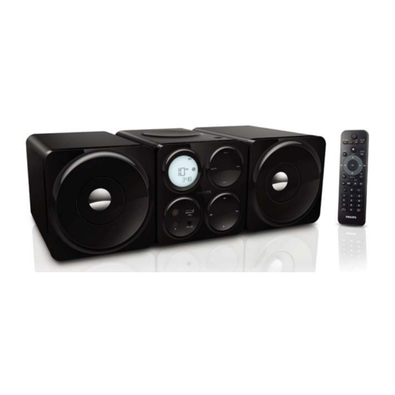
Micro Audio System
Contents
.................................................1-1 to 1-10
2 Laser Beam Safety Precautions......................................... 2-1
3 Important Safety Precautions .................................. 3-1 to 3-2
4 Safety Check After Servicing ............................................. 4-1
5 Safety Information General Notes & Lead Free
Requirements .................................................................... 5-1
7 Direction of Use ....................................................... 7-1 to 7-2
8 Cabinet Disassembly Instructions ........................... 8-1 to 8-2
9 Troubleshooting ....................................................... 9-1 to 9-2
10 Block Diagram .................................................................10-1
11 Wiring Diagram ...............................................................11-1
Circuit Diagram .......................................12-1 to 12-2
Layout Diagram ...................................................12-3
13 Display Board
Circuit Diagram ................................................12-4
Layout Diagram ...............................................12-5
14 Power Board
Circuit Diagram .................................................12-6
Layout Diagram.................................................12-7
© Copyright 2012 Philips Consumer Electronics B.V. Eindhoven, The Netherlands.
All rights reserved. No part of this publication may be reproduced, stored in a
retrieval system or transmitted, in any form or by any means, electronic,
mechanical, photocopying, or otherwise without the prior permission of Philips.
Published by LX-KM 1210 AVM
Version 1.0
Page
Printed in the Netherlands
Contents
14 Decoder Board
Circuit Diagram ......................................... 12-8 to 12-13
Layout Diagram ............................................... 12-14
15 Exploded View....................................................................13-1
16 Revision List .......................................................................14-1
Features
RDS
Voltage Selector
ECO Standby
DTS
Subject to modi cation
MCD1065/51/98
Page
Feature
Different /51
/98
EN
3141 785 37610
Advertisement
Table of Contents

Related Manuals for Philips MCD1065/51/98


Summary of Contents for Philips MCD1065/51/98
-
Page 1: Table Of Contents
Feature Different /51 Features © Copyright 2012 Philips Consumer Electronics B.V. Eindhoven, The Netherlands. All rights reserved. No part of this publication may be reproduced, stored in a Voltage Selector retrieval system or transmitted, in any form or by any means, electronic, ECO Standby mechanical, photocopying, or otherwise without the prior permission of Philips. -
Page 2: Technical Specification And Connection Facilities
Technical Specification and Connection Facilities 1.Location of PC Boards Display Board DVD Loader Decoder Board Power Board AMP Board Version Variations Type /Versions: MCD1065 Service policy Board in used: AMP Board Decoder Board Display Board Power Board Type /Versions MCD1065 Feature diffrence Features VOLTAGE SELECTOR... - Page 3 Technical Specification and Connection Facilities 2. General Information and Requirement Product Family Features 2.1.1 Identity and Key Features MCD1065 series are Micro DVD Audio System, DVD/CD/MP3 play, USB, Tuner FM(20presets), Elements to include as generic requirements: 1. Detachable mains cord 2.
- Page 4 Technical Specification and Connection Facilities Model MCD1065 iPod dock with Authentication chip √ MP3 Link √ (3.5mm audio jack) Composite CVBS √ (Yellow) Component Y Pb Pr √ Aux In √ (RCA cinch) Aux Out √ (RCA cinch) Tuner Socket √...
- Page 5 Technical Specification and Connection Facilities Quickly guide Mechanical General Information The product appearances and functions are defined in their respective MUS. Product management approves the MUS and it is a leading document where product appearance is applicable. Please refer to Sh560 for mechanical information. Safety Standards Where applicable: For /12 (EU), /05 (UK), /51 (Russia)
- Page 6 Technical Specification and Connection Facilities For air discharge: Level General (kV) USA (kV) Requirement No deviations allowed. >4-8 >6-8 Short perceptible deviations allowed. >15-18 No loss of stored data allowed. General requirement: 1. 10 arcs for positive and negative polarity for unit “on” and “off” for 1kV incremental steps. 2.
- Page 7 Technical Specification and Connection Facilities 3. Technical Specifications Power Supply 3.1.1 Type and versions Build-inSMPS will be used for all models and stroke versions. All using figure built in power cord: Versions Region/Country SMPS Detachable mains cords 12 / 05 EUROPE / UK EU (/12) round 2-pin &...
- Page 8 Technical Specification and Connection Facilities Common mode: 6kV/2 ohm criteria C for Europe. 6kV/12 ohm criteria C for Nafta. Parameters: Ring-wave (100kHz) From +/3kV to +/-6kV in steps of 1 kV. 10 shots per combination. One shot per minute. Serial impedance: 2 Ohm for Europe, 12Ohm for Nafta Polarity and phase: Positive (phase 90º) &...
- Page 9 Technical Specification and Connection Facilities Technical Description 3.2.1 Audio Performance Output Stage Protection: Temperature : Short Circuit: v i t Electrical Data Limit Normal DSC: Channel Difference: ± 3dB DBB: Hum (Vol --- Vol -20dB) 150nW Bass: Residual Noise(Volume Minimum) 40nW Treble: Channel Seperation:...
- Page 10 Technical Specification and Connection Facilities 3.2.2 Video Performance 3.2.2.1 CVBS Description Test Signal Specification NTSC Amplitude output 100% White 1Vpp ± 10% 1Vpp ± 10% ± ± i l p ± ± 75% Color bar 286mV, +1dB / - 300mV, +1dB / - Burst Amplitude Burst / chroma ratio 100% Color bar...
- Page 11 Technical Specification and Connection Facilities TUNER FM use Silicon Lab Si4704/4705(w/RDS) GENARAL PART WAVE RANGE VERSION TOLERANCE TUNING GRID FM 87.5 – 108.00 MHz QUARTZ PRECISION 50kHz AERIAL : PIG TAIL ANT WIRE 75Ω ELECTRICAL DATA i t i t i v Search time digital tuning system.
-
Page 12: Laser Beam Safety Precautions
Laser Beam Safety Precautions This Blu-Ray player uses a pickup that emits a laser beam. Do not look directly at the laser beam coming from the pickup or allow it to strike against your skin. The laser beam is emitted from the location shown in the figure. When checking the laser diode, be sure to keep your eyes at least 30 cm away from the pickup lens when the diode is turned on. -
Page 13: Important Safety Precautions
Do not insert warped or cracked discs into the disc compartment. the combined weight of the product and the wall mount. Koninklijke Philips Remove discs from the disc compartment if you are not using the product for an Electronics N.V. bears no responsibility extended period of time. - Page 14 Important Safety Precautions Disposal of your old product and batteries Your product is designed and manufactured with high quality materials and components, which can be recycled and reused. When this crossed-out wheeled bin symbol is attached to a product it means that the product is covered by the European Directive 2002/96/EC.
- Page 15 Safety Check after Servicing Examine the area surrounding the repaired location for damage or deterioration. Observe that screws, parts, and wires have been returned to their original positions. Afterwards, do the following tests and confirm the specified values to verify compliance with safety standards. 1.
-
Page 16: Requirements
Safety Information, General Notes & Lead Free Requirements Safety Instructions Warnings General Safety General Safety regulations require that during a repair: All ICs and many other semiconductors are susceptible to Connect the unit to the mains via an isolation transformer. electrostatic discharges (ESD, ). -
Page 17: Standard Notes For Servicing,Lead Free Requirements & Handling Flat Pack Ic
When soldering, be sure to use the Pb free solder. indicated as shown. Information about lead-free soldering Top View Bottom View Philips CE is producing lead-free sets from 1.1.2005 onwards. Input IDENTIFICATION Regardless of special logo (not always 2. For other ICs, pin 1 and every fifth pin are indicated) indicated as shown. - Page 18 2004), containing leaded solder-alloy and components, all needed spare-parts will be available till the end of the service-period. For repair of such sets nothing changes. On our website www.atyourservice.ce.Philips.com you find more Fig. S-1-1 information to: BGA-de-/soldering (+ baking instructions) 2.
- Page 19 Standard Notes for Servicing, Lead Free Requirements & Handling Flat Pack IC 3. The flat pack-IC on the CBA is affixed with glue, so 4. Release the flat pack-IC from the CBA using be careful not to break or damage the foil of each tweezers.
- Page 20 Standard Notes for Servicing, Lead Free Requirements & Handling Flat Pack IC Instructions for Handling Semi- 2. Installation conductors 1. Using desoldering braid, remove the solder from the foil of each pin of the flat pack-IC on the CBA Electrostatic breakdown of the semi-conductors may so you can install a replacement flat pack-IC more occur due to a potential difference caused by easily.
-
Page 21: Direction Of Use
The following excerpt of the DFU/QSG serves as an introduction to the set. The Complete Direction for Use can be download in different languages from the internet site of Philips Customer care Center : www.support.philips.com Overview of the main unit... - Page 22 Direction of Use Connect TV • Search in a track or disc. • Fast backward or forward. Connect through composite video • For menus, navigate left/right. Connect the supplied composite video cable to: • Rotate a picture. • the VIDEO OUT socket on this unit. •...
-
Page 23: Cabinet Disassembly Instructions
Cabinet Disassembly Instructions Note: 1. Disassembly Flowchart (1) Identification (location) No. of parts in the figures This flowchart indicates the disassembly steps to gain (2) Name of the part access to item(s) to be serviced. When reassembling, (3) Figure Number for reference follow the steps in reverse order. - Page 24 Cabinet Disassembly Instructions Fig. D6 Fig. D3 Fig. D4 Fig. D5...
-
Page 25: Troubleshooting
Troubleshooting FLOW CHART NO.1 No sound from whole unit check if speaker is ok check and change speaker and output wire check if public circuit of whole unit check radio tube and periphery circuit AMP circuit is ok check and change transormer of power supply and check if power supply circuit of whole unit is ok power commutate circuit... - Page 26 Troubleshooting no search from DVD check if supply +12V of Decoding board is normal check steady circuit check if laser head ass'y can light normally Decoding board is broken check if tie wires of laser head ass'y check and change good laser head ass'y is loosen and broken laser head ass'y broken FLOW CHART NO.4...
-
Page 27: Block Diagram
Block Diagram 89S_3V3 V1.8V CVBS CVBS_OUT S3 3V S3.3V SDRAM CMS-S76 M3.3V K4S641632H-UC60 DVD_5V RFS3 MAIN CHIPSET F3.3V MT1389DXE-J si4702 LOADER MOTOR DRIVER FLASH CD5954CB EN29LV160AB-70TCP E3.3V WXD-8829E WXD 8829E MP3 Link SERIAL EEPROM 24C16 DVD_5V DVD/CD_RL D-/D+ HP_OUT MP3_LR_IN (host 2.0) LCD DISPLAY MCU3.3V... -
Page 28: Wiring Diagram
Wiring Diagram AMP Board DVD Loader Decoder Board Display Board 11-1 11-1... - Page 29 AMP Board -- Circuit Diagram 1 R113 R120 MP3_L SI4702/03 A18V MP3_R 9.1V CB34 CB35 CB36 CB37 CB38 330R/1W SI4704/05 120nH 33PF 33PF NC/33PF 33PF 33PF 9.1V MP3_L 4.7uF CB39 CB40 CB41 CB42 CB43 BD3491 MP3_R 4.7uF BD3491FS 9.1V 33PF 33PF NC/33PF 33PF...
- Page 30 AMP Board -- Circuit Diagram 2 MCU3.3V/IP5V R229 0R NC/HT7333 R246 470 1/2W 8V_IN MCU3.3V OUT1 SOT89 C134 CE41 100u/16V 0.1uF EJS89J2010 AP1538/SOP-8 8V_IN SOP8/SMD CES2307 L71 47UH-3A L66 DCR 33R SOT23A L70 FB_0349 R233 + CE40 C138 C139 R255 R254 4.7K 24.9k-1%...
- Page 31 AMP Board -- Layout Diagram 12-3 12-3...
- Page 32 Display Board -- Circuit Diagram SMARK SMARK SMARK SMARK 120K COM[00:07] MP3_R 3.3V AUTO-OFF AGND SEG[00:23] MP3_R 47uF/6.3V 100P MP3_L AGND TE-03575 MP3_L CON1 2.0-3P 100R SEG11 DATA SG12 100R SEG12 SG13 100R SEG13 SG14 3.3V SEG14 SG15 SEG15 SG16 560R SEG16 I-PT6533...
- Page 33 Display Board -- Layout Diagram 12-5 12-5...
- Page 34 Power Board -- Circuit Diagram T2AL250V JUMPER UU9.8-30MH CON1A 1N4007 1N4007 2PIN MOV1 103P,1KV 103/1KV 47uF,400V CON2 XH2.54-3PIN 1N4007 1N4007 HGND 9V 4A SB3100 2.2uH,3*15mm SB3100 EE22 22R,1206 103P,630V 1nF,50V,0805 2200uF,10V 1000uF,10V 0R,0805 22R,1206 FR107 3.3V 5.1R,0805 FR107 HGND DRV2 DRV1 68R,0805 4N60...
- Page 35 Power Board -- Layout Diagram 12-7 12-7...
- Page 36 Decoder Board -- Circuit Diagram 1 MT1389J General GPIO List Name Features COMMON1389J_HD850_AM5888_STBY OFF-PAGE CONNECTION GPO5 TRCLOSE MT1389J DVD Board w/ Sanyo HD6x Series PUHs MDI1 VR_CD GPO_B VR_DVD GPIO2 TRIN 1 INDEX & POWER / RESET UP1_6 VSCK UP1_7 VSDA 2 MT1389J LQFP128 GPIO11...
- Page 37 Decoder Board -- Circuit Diagram 2 SERVO RF DeCAP. OFF-PAGE CONNECTION 89J_3V3 RFV12-2 RFV12-1 89J_3V3 DQ[0..15] Crystal DQ[0..15] RFVDD3 MA[0..11] MA[0..11] DV33 ADACVDD 100k FB/200 0.1uF 0.1uF 4.7uF 10u/10V 0.1uF DQM[0..1] DQM[0..1] BAT54C AADVDD DACVDD3 27MHz BA[0..1] BA[0..1] 0.1uF SP-A close to 89J IC DCLK DCLK...
- Page 38 Decoder Board -- Circuit Diagram 3 OFF-PAGE CONNECTION ESMT M12L64164A DV33 SR_3V3 DQ[0..15] DQ[0..15] MA[0..11] MA[0..11] CB20 DQM[0..1] DQM[0..1] 0.1uF SR_3V3 BA[0..1] BA[0..1] SDCKE DCLK DCLK DCS# MA10 DQ10 RAS# RAS# A10/AP DQ10 MA11 DQ11 CAS# CAS# DQ11 SR_3V3 10pF/NC DBA0 DQ12 BA0/A13...
- Page 39 Decoder Board -- Circuit Diagram 4 OFF-PAGE CONNECTION +5VV +5VV default: Low Impedance Mode CVBS_OUT CVBS_OUT CB28 CB29 +5VV 0.1uF 0.1uF 3.3K 3.3K CD11X/100uF16V CD11X/22UF16V L16 1.8uH/SMD L17 1.8uH/SMD CVBS_OUT CE16 CE17 2N3904 2N3904 L73 FB L67 FB VIDEO_DVD G/Y/DVD R237 R244 CE18...
- Page 40 Decoder Board -- Circuit Diagram 5 R113 R120 SI4702/03 CON1 IPOD_DET SI4704/05 120nH IPOD_RX IPOD_TX IPOD_ACCDET ECO_POWER NC/0R ECO_POWER R_IPOD_BT NC/FB1K IPOD_R AV2-8.4-13D L_IPOD_BT NC/FB1K IPOD_L 4.7uF DVD_ON DVD_ON AUX_L DIP1.0MM-8 AUX_R 4.7uF NC/1.0A-8PL 0.01uF 0.01uF 100pf 100pf DOUT NC/0R 680pF 680pF A18V...
- Page 41 Decoder Board -- Circuit Diagram 6 MCU3.3V/IP5V R229 0R NC/HT7333 18V_IN MCU3.3V OUT1 R246 470 1/2W SOT89 C134 CE41 100u/16V 0.1uF C142 10uF EJS89J2010 AP1538/SOP-8 SOT23A 18V_IN SOP8/SMD CES2307 L70 FB_0349 L71 47UH-3A L66 DCR 33R + CE40 C138 C139 R233 R255 R254...
- Page 42 Decoder Board -- Layout Diagram 12-14 12-14...
- Page 43 Exploded View S106 S111 S101 S105 Light-Guide Ringe(PMMA) S104 S108 S110 S107 Screw S109 Gear Bracket CD Door Gear PCB2 Screw PCB4 IR Receiver Bracket PCB1 Screw Screw Screw PCB3 S100 Bottom Cover Rubber Foot 13-1 13-1...
- Page 44 Revision List Revision List Version 1.0 * Initial Release 14-1...