Table of Contents
Advertisement
Quick Links
SERVICE MANUAL
Ver 1.0 2002. 03
This set is the tuner, CD and amplifier
section in CMT-L1.
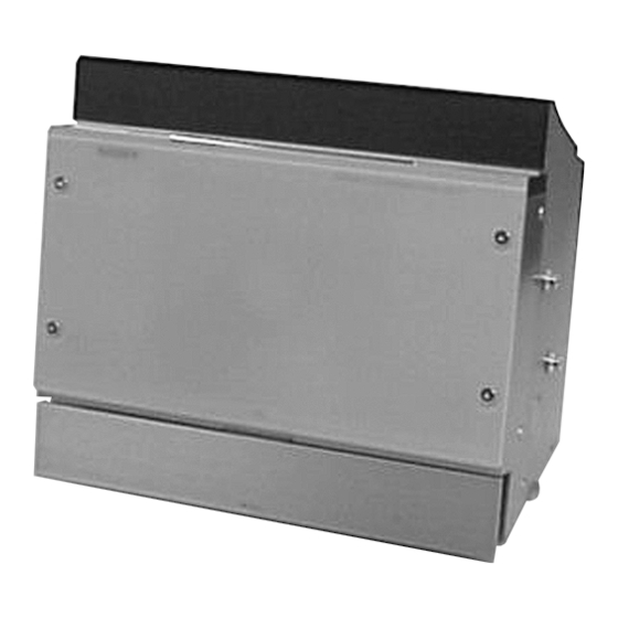
Main unit (HCD-L1)
Amplifier section
For the U.S. model
AUDIO POWER SPECIFICATIONS
POWER OUTPUT AND TOTAL
HARMONIC DISTORTION:
With 4-ohm loads, both channels driven, from
120 - 10,000 Hz; rated 25 watts per channel
minimum RMS power, with no more than 10%
total harmonic distortion from 250 milliwatts to
rated output.
North American model:
Continuous RMS power output (reference):
European model:
DIN power output (rated): 20 + 20 W
Continuous RMS power output (reference):
Music power output (reference):
Other models:
The following measured at 220 V AC, 60 Hz
DIN power output (rated): 20 + 20 W
Continuous RMS power output (reference):
Sony Corporation
9-873-561-01
2002C1600-1
Home Audio Company
© 2002.03
Published by Sony Engineering Corporation
Model Name Using Similar Mechanism
CD
CD Mechanism Type
SECTION
Base Unit Type
SPECIFICATIONS
Inputs
MD/TAPE IN (stereo minijack):
Outputs
MD/TAPE OUT (stereo minijack):
PHONES (stereo minijack):
DIGITAL CD OPTICAL OUT (Supported sampling
frequency: 44.1 kHz)
CD player section
System
25 + 25 W
(4 ohms at 1 kHz, 10%
Laser
THD)
(4 ohms at 1 kHz, DIN)
Frequency response
25 + 25 W
Tuner section
(4 ohms at 1 kHz, 10%
THD)
FM stereo, FM/AM superheterodyne tuner
FM tuner section
25 + 25 W
Tuning range
North American model:
Other models:
(4 ohms at 1 kHz, DIN,
110 V - 240 V AC)
Antenna
Antenna terminals
25 + 25 W
Intermediate frequency
(4 ohms at 1 kHz, 10%
THD, 110 V - 240 V AC)
MICRO Hi-Fi COMPONENT SYSTEM
HCD-L1
US Model
Canadian Model
AEP Model
UK Model
E Model
NEW
CDM71A
BU-31BD63A
Sensitivity 450 mV (MD)/
250 mV (Tape),
impedance 47 kilohms
Sensitivity 250 mV,
impedance 1 kilohmes
Accepts headphones with
an impedance of 8 ohms
or more
Compact disc and digital
audio system
Semiconductor laser
(λ = 795 nm)
Emission
duration: continuous
2 Hz – 20 kHz
87.5 - 108.0 MHz
(100-kHz step)
87.5 - 108.0 MHz
(50-kHz step)
FM wire antenna
75 ohm unbalanced
10.7 MHz
— Continued on next page —
Advertisement
Table of Contents

Related Manuals for Sony HCD-L1


Summary of Contents for Sony HCD-L1
- Page 1 Intermediate frequency 10.7 MHz (4 ohms at 1 kHz, 10% THD, 110 V - 240 V AC) — Continued on next page — MICRO Hi-Fi COMPONENT SYSTEM Sony Corporation 9-873-561-01 2002C1600-1 Home Audio Company © 2002.03 Published by Sony Engineering Corporation...
- Page 2 HCD-L1 SAFETY CHECK-OUT AM tuner section Tuning range North American model: 530 - 1,710 kHz After correcting the original service problem, perform the (with the tuning interval set at 10 kHz) following safety checks before releasing the set to the customer: 531 - 1,710 kHz Check the antenna terminals, metal trim, “metallized”...
-
Page 3: Table Of Contents
HCD-L1 TABLE OF CONTENTS 1. SERVICING NOTES 6. DIAGRAMS ······················································· 4 6-1. Block Diagrams CD Section ····································· 23 2. GENERAL MAIN Section ···························································· 24 ·········································································· 5 6-2. Circuit Boards Location ············································· 25 6-3. Printed Wiring Board BD Section (Side A) ·············· 26 3. -
Page 4: Servicing Notes
30 cm away from the objective lens. DIAGRAMMES SCHÉMATIQUES ET LA LISTE DES PIÈCES SONT CRITIQUES POUR LA SÉCURITÉ DE FONCTIONNEMENT. NE REMPLACER CES COMPOSANTS QUE PAR DES PIÈSES SONY Laser component in this product is capable DONT LES NUMÉROS SONT DONNÉS DANS CE MANUEL OU DANS LES SUPPÉMENTS PUBLIÉS PAR SONY. -
Page 5: General
HCD-L1 SECTION 2 This section is extracted GENERAL from instruction manual. List of Button Locations and Reference Pages Illustration number How to use this page Use this page to find the location of buttons and other PLAY MODE qg (9, 13, 14) parts of the system that are mentioned in the text. - Page 6 HCD-L1 Remote control ALPHABETICAL ORDER BUTTON DESCRIPTIONS @/1 (power) 4 (8, 19) L – Z A – F ./> qa (10 - 14, 19) CD N wd (11 - 13) Letter/Numeric buttons wg (12, m/M wf (11) 13, 16) CD X ws (11) Z 1 (11) MENU/NO q;...
- Page 7 HCD-L1 Replacing the battery in Setting the clock the remote Turn on the system. Slide out and remove the battery case. Press CLOCK/TIMER SET on the remote. Press . or > on the remote repeatedly to set the day, and then press ENTER/YES or CURSORt on the remote.
-
Page 8: Disassembly
HCD-L1 SECTION 3 DISASSEMBLY • The equipment can be removed using the following procedure. BOTTOM PLATE,CASE FRONT PANEL SECTION SET (HCD-L1) (Page 9) (Page 9) AMP BOARD, POWER BOARD, MAIN BOARD REGURATOR AM/FM Tuner (Page 10) (Page 11) (Page 10) -
Page 9: Bottom Plate,Case
HCD-L1 Note : Follow the disassembly procedure in the numerical order given. 3-1. Bottom Plate,Case qg case qd three claws 6 t wo screws (SS) 5 f our screws (SS) 7 s crew (+PTT 3 × 6 ) qf c onnector... -
Page 10: Power Board, Am/Fm Tuner
HCD-L1 3-3. POWER Board, AM/FM Tuner 2 two screws (+BVTP 3 × 8) 4 POWER board 1 connector (CN800) 3 connector (CN500) 7 AM/FM t uner 6 flat type wire (11core or 15core) 5 two screws (+BVTP 3 × 8) 3-4. -
Page 11: Amp Board, Regurator
HCD-L1 3-5. AMP Board, Regurator q; four screws (+BVTP 3 × 8) qa connector 6 two claws qf screw (+BVTP 3 × 8) 1 connector (CN300) qg screw (+BVTP 3 × 8) qh regurator 2 two screws (+BVTP 3 × 8) qd two screws (+BVTP 3 ×... -
Page 12: Led Board (L)
HCD-L1 3-7. LED Board (L) 4 t wo screws (+BVTP 2.6 × 8) 1 connector (CN1302) 5 LED board (L) 3 holder (LED-L) 2 screw (+BTP 2.6 × 6) 3-8. FL (L1) Board 2 FL(L1) board 1 t wo screws (+BVTP 2.6 × 8) -
Page 13: Switch Board, Touch Switch Board
HCD-L1 3-9. SWITCH Board, TOUCH SWITCH Board 3 TOUCH SWITCH board 2 t wo screws (+BVTP 2.6 × 8) 1 c onnector (CN1302) 6 SWITCH board 4 c onnector (CN1303) 5 f ive screws (+BVTP 2.6 × 8) 3-10. CD Board 6 bracket (CD-MT) 5 two screws (+BVTP 3 ×... -
Page 14: Cd-Mechanism (Cdm71A)
HCD-L1 3-11. CD-Mechanism (CDM71A) 5 CD mechanism (CDM71A) 1 t wo screws (+BVTP 2.6 × 8) 4 blacket 2 t wo screws (+BVTP 2.6 × 8) 3 six screws (+BVTP 2.6 × 8) 3-12. L.MOTOR Board Remove solder (two portions ). -
Page 15: Encoder Board, D.sensor Board
HCD-L1 3-13. ENCODER Board, D.SENSOR Board 3 screw 4 D.SENSOR board (+BTP M 2.6 × 6) 1 screw (+PWH,2X6) 2 ENCODER board 3-14. RTL Pulley Assy Disengage the claw and rotate the RTL pulley assy in the direction of , and remove your hands at the position where the shaft agrees with the hole shape on the chassis. -
Page 16: Bd Board
HCD-L1 3-15. BD Board Remove solder (two portions ). (BLK) 6 BD board (RED) 3 screw 5 h ook 4 flxible board Remove solder (two portions ). 3-16. C MOTOR Board, L.SENSOR Board 4 Connector (CN711) 7 Connector Remove solder (CN754) (two portions ). -
Page 17: Base Unit
HCD-L1 3-17. Base Unit (BU-31BD63A) Rotate the SPT pulley assy in the direction of to move the Base unit shaft forward. 2 screw (+PTPWH M2.6) 5 base unit (BU-31BD) SPT pulley assy shaft shaft 8 screw 3-18. Holder Assy, Sled Motor Assy (+PTPWH M2.6) -
Page 18: Rtr Pulley Assy
HCD-L1 3-19. RTR Pulley Assy Disengage the claw and rotate the RTR pulley assy in the direction of , and remove your hands at the position where the shaft agrees with the hole shape on the chassis. RTR pulley assy... -
Page 19: Test Mode
HCD-L1 SECTION 4 TEST MODE [Key Check Mode] [Amp Test Mode] * Keyboard check. * Combinatin of preset equalizer and volume is changed for the Procedure: amplifier test. Press the ?/1 button to turn the set ON. Procedure: To enter the test mode, press three buttons DISPLAY , NX Press the ?/1 button to turn the set ON. - Page 20 HCD-L1 [Error History Display Mode] DISPLAY : “ E**M##%%0000 “ Procedure: : order of mechanism error happens (hexadecimal) Setting Method of Test Mode 00 : the newest error Press the ?/1 button to turn the set ON. 09 : the error ten times before Select the FUNCTION to CD.
- Page 21 HCD-L1 Reset of No Disc Error History Select the operation in the menu by pressing the . or > button to display “dvt ECONT0 BU”. Press the CD PLAY button. No disc error history is reset. Reset of Error History Select the operation in the menu by pressing the .
-
Page 22: Electrical Adjustments
HCD-L1 SECTION 5 ELECTRICAL ADJUSTMENTS Adjustment Location : CD SECTION Note : [ BD (CD) BOARD ] — SIDE A — 1. CD Block is basically designed to operate without adjustment. Therefore, check each item in order given. 2. Use YEDS-18 disc (3-702-101-01) unless otherwise indicated. -
Page 23: Diagrams
HCD-L1 SECTION 6 DIAGRAMS 6-1. Block Diagrams CD Section Q103,D101 Q601 Q1411 +3.3V • R-CH is omitted due to same as L-CH. BD+3.3V SWITCH D+5V D+3.3V SWITCH • Signal Path BD+5V : CD (DIGITAL) IC1410 384Fs OSC Q602 : CD (ANALOG) -
Page 24: Main Section
HCD-L1 MAIN Section IC711 SOUND PROCESSOR J700 MD/TAPE INEX1 R-CH IC731 IC301 MUTING Q701 J701 S-MASTER MD/TAPE IC370 INA1 OUT1 L-IN DOUT DATA R-CH POWER AMP PDWN LRCK LRCK J301 SCKI OUTR2+ OUTA IC745 CLOCK DRIVER OUTR1+ OUTB SPEAKER DAOUT-L... -
Page 25: Circuit Boards Location
HCD-L1 6-2. Circuit Boards Location THIS NOTE IS COMMON FOR PRINTED WIRING • Indication of transistor BOARDS AND SCHEMATIC DIAGRAMS. (In addition to this, the necessary note is printed in each block.) These are omitted. For schematic diagrams. POWER board Note: •... -
Page 26: Printed Wiring Board Bd Section (Side A)
HCD-L1 6-3. Printed Wiring Board BD Section (Side A) • See page 25 for Circuit Boards Location. (Page 31) IC106 IC101 (BLK) TP(DVC) (RED) TP(TE) IC103 IC102 TP(RFAC) • Semiconductor Location Ref. No. Location IC101 IC102 IC103 IC106 Q101... -
Page 27: Printed Wiring Board Bd Section (Side B)
HCD-L1 6-4. Printed Wiring Board BD Section (Side B) • See page 25 for Circuit Boards Location. • Semiconductor Location Ref. No. Location D101 D201 Q103... -
Page 28: Schematic Diagram Bd Section
HCD-L1 6-5. Schematic Diagram BD Section • See page 41 for Wavefoms. • See page 41 for IC Block Diagrams. IC B/D IC B/D (Page 29) -
Page 29: Schematic Diagram Cd Section
HCD-L1 6-6. Schematic Diagram CD Section • See page 41 for Wavefoms. • See page 41 for IC Block Diagrams. • See page 49 for IC Pin Function Description. IC B/D (Page 37) (Page 28) D1412 1SS355TE D1413 1SS355TE R609... -
Page 30: Printed Wiring Board Cd Section (Side A)
HCD-L1 6-7. Printed Wiring Board CD Section (Side A) • See page 25 for Circuit Boards Location. (Page 32) (Page 34) (Page 32) IC1431 (Page 34) • Semiconductor Location Ref. No. Location D1411 IC1431 Q1411... -
Page 31: Printed Wiring Board Cd Section (Side B)
HCD-L1 6-8. Printed Wiring Board CD Section (Side B) • See page 25 for Circuit Boards Location. IC600 • Semiconductor Location Ref. No. Location IC1400 D635 IC1410 IC600 IC1400 IC1410 Q600 Q601 Q602 Q651 (Page 26) -
Page 32: Printed Wiring Board Motor Section
HCD-L1 6-9. Printed Wiring Board MOTOR Section • See page 25 for Circuit Boards Location. IC721 IC701 (CK) IC731 (Page 30) (Page 30) (LO) IC711... -
Page 33: Schematic Diagram Motor Section
HCD-L1 6-10. Schematic Diagram MOTOR Section (Page 29) (Page 29) -
Page 34: Printed Wiring Board Main Section (Side A)
HCD-L1 6-11. Printed Wiring Board MAIN Section (Side A) • See page 25 for Circuit Boards Location. • Semiconductor Location IC791 Ref. No. Location D501 D502 DIGITAL CD D709 OPTICAL OUT (Page 38) D771 IC500 IC580 IC711 IC791 Q571 Q572... -
Page 35: Printed Wiring Board Main Section (Side B)
HCD-L1 6-12. Printed Wiring Board MAIN Section (Side B) • See page 25 for Circuit Boards Location. IC731 IC745 • Semiconductor Location Ref. No. Location D535 D593 D731 D732 IC731 IC745 Q500 Q525 Q526 Q527 Q761 Q789... -
Page 36: Schematic Diagram Main Section (1/2)
HCD-L1 6-13. Schematic Diagram MAIN Section (1/2) • See page 41 for Wavefoms. (Page 40) D792 1SS355TE 1SS355TE D793... -
Page 37: Schematic Diagram Main Section (2/2)
HCD-L1 6-14. Schematic Diagram MAIN Section (2/2) • See page 41 for Wavefoms. • See page 48 for IC Pin Function Description. (Page 47) (Page 29) C700 0.001 EP700 C750 (Page 29) (Page 45) (Page 43) -
Page 38: Printed Wiring Board Amp Section (Side A)
HCD-L1 6-15. Printed Wiring Board AMP Section (Side A) • See page 25 for Circuit Boards Location. (Page 44) • Semiconductor Location Ref. No. Location D360 D380 IC305 IC333 IC350 IC370 Q396 (Page 34) Q400 Q401 Q450 Q451 Q470 Q471... -
Page 39: Printed Wiring Board Amp Section (Side B)
HCD-L1 6-16. Printed Wiring Board AMP Section (Side B) • See page 25 for Circuit Boards Location. IC301 IC401 • Semiconductor Location Ref. No. Location D350 D351 D352 D361 IC300 D362 D370 D371 D372 D381 D382 IC300 IC301 IC401 Q391... -
Page 40: Schematic Diagram Amp Section
HCD-L1 6-17. Schematic Diagram AMP Section • See page 41 for Wavefoms. (Page 36) (Page 45) 0.001 0.001 0.001 0.001 C390 0.01... -
Page 41: Ic Block Diagrams
HCD-L1 6-18. IC Block Diagrams – BD BOARD – • WAVEFORMS IC101 CXD3068Q IC103 CXA2581N-T4 IC101 us (XTAO) IC500 ek (X2) RW/ROM DC OFST RFDCI – – 5.8 Vp-p RFDCO 59 ns 3.9 Vp-p 50 ns 1V/DIV,20ns/DIV 1V/DIV,20ns/DIV IC600 ek (X2) IC745 2 –... -
Page 42: Printed Wiring Board Display Section
HCD-L1 6-19. Printed Wiring Board DISPLAY Section • See page 25 for Circuit Boards Location. IC1201 (Page 34) • Semiconductor Location Ref. No. Location D1281 D1282 D1283 D1284 D1285 IC1201 Q1201 Q1281 Q1282... -
Page 43: Schematic Diagram Display Section
HCD-L1 6-20. Schematic Diagram DISPLAY Section • See page 41 for Wavefoms. (Page 37) -
Page 44: Printed Wiring Board Swtich Section
HCD-L1 6-21. Printed Wiring Board SWITCH Section • See page 25 for Circuit Boards Location. • Semiconductor Location Ref. No. Location D1311 D1321 D1322 D1323 D1326 IC1361 IC1362 D1361 IC1351 D1362 D1363 D1364 D1381 D1382 D1391 D1392 IC1351 IC1361 IC1362... -
Page 45: Schematic Diagram Swtich Section
HCD-L1 6-22. Schematic Diagram SWTICH Section • See page 41 for IC Block Diagrams. (Page 37) IC B/D (Page 40) -
Page 46: Printed Wiring Board Power Section
HCD-L1 6-23. Printed Wiring Board POWER Section • See page 25 for Circuit Boards Location. IC803 • Semiconductor IC802 IC801 Location Ref. No. Location IC800 IC 800 IC 801 IC 802 IC 803 IC 804 D801 IC804 D802 D803 D804... -
Page 47: Schematic Diagram Power Section
HCD-L1 6-24. Schematic Diagram POWER Section 4.7k 2.2k 1/2W (Page 37) -
Page 48: Ic Pin Function Description
HCD-L1 6-25. IC PIN FUNCTION DESCRIPTION • IC500 uPD703033AYGF-M34-3BA (MASTER CONTROL) (MAIN BOARD) Pin No. Pin Name Description Pin No. Pin Name Description FL-DATA Data output for display SOFT CHECK1 Main operation check terminal FL-CLK Clock output for display SOFT CHECK2... - Page 49 HCD-L1 • IC600 uPD703033AYGF-M34-3BA (CD CONTROL) (CD Board) Pin No. Pin Name Description DACDAT DAC data output DACCLK DAC clock output IICDATA 12C bus data input/output — Not used IICCLK 12C bus clock input/output — Not used DATA Data output for CXD30689...
- Page 50 HCD-L1 Pin No. Pin Name Description D.SENS.OUT D sensor output LOD1POS Loading motor output (+) LOD1NEG Loading motor output (-) LOD2POS Chucking motor output (+) LOD2NEG Chucking motor output (-) 56,57 — Not used BVDD — +5 V power terminal BVSS —...
-
Page 51: Exploded Views
HCD-L1 SECTION 7 EXPLODED VIEWS NOTE: • -XX, -X mean standardized parts, so they may • The mechanical parts with no reference number The components identified by mark 0 or have some differences from the original one. in the exploded views are not supplied. -
Page 52: Chassis Section
HCD-L1 7-2. Chassis Section not supplied F901 not supplied not supplied not supplied not supplied not supplied front panel section Ref. No. Part No. Description Remarks Ref. No. Part No. Description Remarks A-4728-100-A MAIN BOARD, COMPLETE (AEP,UK) A-4728-117-A POWER BOARD, COMPLETE... -
Page 53: Front Panel Section
HCD-L1 7-3. Frot Panel Section not supplied not supplied not supplied CD mechanism section (CDM71A) not supplied Ref. No. Part No. Description Remarks Ref. No. Part No. Description Remarks 4-238-506-01 INDICATOR (BS) A-4728-112-A FL (L1) BOARD, COMPLETE 4-951-620-01 SCREW (2.6X8), +BVTP... -
Page 54: Mechanism Section(Cdm71A)-1
HCD-L1 7-4. Mechanism Section(CDM71A)-1 mechanism section M711 supplied (CDM71A)-2 M701 not supplied not supplied not supplied not supplied not supplied not supplied Ref. No. Part No. Description Remarks Ref. No. Part No. Description Remarks 4-951-620-01 SCREW (2.6X8), +BVTP 1-683-915-12 L.MOTOR BOARD... -
Page 55: Mechanism Section(Cdm71A)-2
HCD-L1 7-5. Mechanism Section(CDM71A)-2 supplied supplied base unit (BU-31BD63A) Ref. No. Part No. Description Remarks Ref. No. Part No. Description Remarks X-4954-292-1 PULLEY (SPT) ASSY 4-218-252-51 SCREW (+PTPWH M2.6), FLOATING 4-237-417-02 CAM (A) X-4954-644-1 GEAR (RT) ASSY 4-238-841-01 BUSHING (GEAR) -
Page 56: Base Unit Section (Bu-31Bd63A)
HCD-L1 7-6. Base Unit (BU-31BD63A) not supplied not supplied not supplied M102 Ref. No. Part No. Description Remarks Ref. No. Part No. Description Remarks 4-218-252-51 SCREW (+PTPWH M2.6), FLOATING 3-729-076-11 SCREW (+B) (2X4) 4-238-914-01 INSULATOR 4-238-865-01 LEVER (SHUTTER) 4-238-661-01 SPRING (HOLDER), TENSION COIL... -
Page 57: Electrical Parts List
HCD-L1 SECTION 8 ELECTRICAL PARTS LIST NOTE: • Due to standardization, replacements in the • RESISTORS When indicating parts by reference number, parts list may be different from the parts All resistors are in ohms. please include the board name. - Page 58 HCD-L1 Ref. No. Part No. Description Remarks Ref. No. Part No. Description Remarks D362 6-500-055-01 DIODE P6SMB33AT3 Q471 8-729-046-97 TRANSISTOR 2SD1938(F)-T(TX).SO D370 6-500-131-01 DIODE LI116 D371 6-500-248-11 DIODE SFPL-62V < RESISTOR > D372 6-500-055-01 DIODE P6SMB33AT3 D380 6-500-131-01 DIODE LI116...
- Page 59 HCD-L1 Ref. No. Part No. Description Remarks Ref. No. Part No. Description Remarks R470 1-216-864-11 METAL CHIP 1/16W C224 1-164-360-11 CERAMIC CHIP 0.1uF R471 1-216-825-11 METAL CHIP 2.2K 1/16W C226 1-164-360-11 CERAMIC CHIP 0.1uF R472 1-216-827-11 METAL CHIP 3.3K 1/16W...
- Page 60 HCD-L1 Ref. No. Part No. Description Remarks Ref. No. Part No. Description Remarks R202 1-216-833-11 METAL CHIP 1/16W C646 1-162-971-11 CERAMIC CHIP 0.001uF 10.00% 50V R203 1-216-845-11 METAL CHIP 100K 1/16W C658 1-164-156-11 CERAMIC CHIP 0.1uF R204 1-216-827-11 METAL CHIP 3.3K...
- Page 61 HCD-L1 C MOTOR D.SENSOR Ref. No. Part No. Description Remarks Ref. No. Part No. Description Remarks < RESISTOR > < COMPOSITION CIRCUIT BLOCK > R601 1-216-809-11 METAL CHIP 1/16W RB614 1-233-576-11 RES, CHIP NETWORK 100 R602 1-216-025-11 METAL CHIP 1/10W...
- Page 62 HCD-L1 ENCODER FL (L1) LED (L) LED (R) Ref. No. Part No. Description Remarks Ref. No. Part No. Description Remarks 1-683-914-11 ENCODER BOARD < COIL > ************** L1281 1-408-080-00 INDUCTOR 100uH S741 1-477-161-11 ENCODER L1282 1-408-072-00 INDUCTOR 47uH ************************************************************ < TRANSISTOR >...
- Page 63 HCD-L1 L. MOTOR L.SENSOR MAIN Ref. No. Part No. Description Remarks Ref. No. Part No. Description Remarks 1-683-915-12 L.MOTOR BOARD C537 1-126-960-11 ELECT 20.00% 50V C538 1-162-974-11 CERAMIC CHIP 0.01uF *************** C539 1-164-156-11 CERAMIC CHIP 0.1uF < CAPACITOR > C540 1-164-156-11 CERAMIC CHIP 0.1uF...
- Page 64 HCD-L1 MAIN Ref. No. Part No. Description Remarks Ref. No. Part No. Description Remarks C755 1-126-964-11 ELECT 10uF 20.00% 50V < IC > C756 1-126-964-11 ELECT 10uF 20.00% 50V (AEP,UK) IC500 6-801-299-01 IC uPD703033AYGF-M34-3BA C757 1-164-156-11 CERAMIC CHIP 0.1uF IC580...
- Page 65 HCD-L1 MAIN Ref. No. Part No. Description Remarks Ref. No. Part No. Description Remarks R535 1-216-841-11 METAL CHIP 1/16W R590 1-216-821-11 METAL CHIP 1/16W R536 1-216-851-11 METAL CHIP 330K 1/16W R591 1-216-841-11 METAL CHIP 1/16W R537 1-216-833-11 METAL CHIP 1/16W...
- Page 66 HCD-L1 MAIN POWER SWITCH Ref. No. Part No. Description Remarks Ref. No. Part No. Description Remarks < COMPOSITION CIRCUIT BLOCK > < RESISTOR > RB515 1-233-576-11 RES, CHIP NETWORK 100 0 R801 1-219-591-11 FUSIBLE 1/2W R802 1-218-871-11 METAL CHIP 0.5% 1/10W <...
- Page 67 HCD-L1 SWITCH TOUCH SWITCH Ref. No. Part No. Description Remarks Ref. No. Part No. Description Remarks < SWITCH > < TRANSISTOR > S1311 1-762-875-21 SWITCH, KEYBOARD (POWER) Q1361 8-729-900-53 TRANSISTOR DTC114EKA-T146 S1313 1-762-875-21 SWITCH, KEYBOARD (DISPLAY) S1314 1-762-875-21 SWITCH, KEYBOARD <...
- Page 68 HCD-L1 REVISION HISTORY Clicking the version allows you to jump to the revised page. Also, clicking the version at the upper right on the revised page allows you to jump to the next revised page. Ver. Date Description of Revision...