Table of Contents
Advertisement
Quick Links
SERVICE MANUAL
• MHC-M500AV is composed of following models.
As for the service manual, it is issued for each component
model, then, please refer to them.
COMPONENT MODEL NAME
COMPACT DISC DECK RECEIVER SYSTEM
FRONT SPEAKER
SPEAKER
SPEAKER
SYSTEM
PACK
SUPER WOOFER
SPECIFICATIONS
General
Power requirements:
120 V AC, 60Hz
Power consumption:
210 watts
Dimensions (w/h/d):
Approx. 280 x 373 x 468 mm
Mass:
Approx. 11.0 kg
Supplied accessories:
AM loop antenna (1)
Remote commander (1)
Batteries (2)
FM lead antenna (1)
Speaker cords (2)
Center speaker pads (4)
Monaural connecting cord (1)
Design and specifications are subject to change without notice.
9-929-284-11
MHC-M500AV
CENTER SPEAKER
SS-RC175D
REAR SPEAKER
Sony Corporation
Audio Entertainment Group
HCD-M500AV
SS-M500AV
SS-CT175D
SS-RS175D
SA-W17
PARTS LIST
Part No.
Description
ACCESSORIES & PACKING MATERIALS
*******************************
1-476-193-11
COMMANDER, STANDARD (RM-SX5)
1-501-374-11
ANTENNA, LOOP
1-501-659-41
ANTENNA (FM)
1-769-433-11
CORD, SPEAKER (10m) (SS-RS175D)
1-751-598-11
MONAURAL CONNECTING CORD ( 2m) (SA-W17)
4-227-898-11
MANUAL, INSTRUCTION (ENGLISH)
4-210-254-01
CUSHION (FOOT)
4-981-643-21
BATTERY COVER (FOR RM-SX5)
COMPACT COMPONENT SYSTEM
US Model
Remark
2000E001613-1D
Printed in Japan ©2000.5
Published by HA Quality Assurance Dept.
Advertisement
Table of Contents

Related Manuals for Sony SS-M500AV


Summary of Contents for Sony SS-M500AV
- Page 1 • MHC-M500AV is composed of following models. As for the service manual, it is issued for each component model, then, please refer to them. COMPONENT MODEL NAME HCD-M500AV COMPACT DISC DECK RECEIVER SYSTEM SS-M500AV FRONT SPEAKER SPEAKER SS-CT175D CENTER SPEAKER SPEAKER...
- Page 2 1 V, impedance 1 kΩ Continuous RMS power output 35 + 35 W (6 Ω at 1 kHz, 10% THD) — Continued on next page — COMPACT COMPONENT SYSTEM 9-929-288-12 Sony Corporation Home Audio Company 2001G0200-1 Shinagawa Tec Service Manual Production Group © 2001.7...
- Page 3 4-track 2-channel stereo Remote commander (1) Frequency response 40 – 13,000 Hz (± 3 dB), Batteries (2) using Sony TYPE I cassette FM lead antenna (1) Speaker cords (2) Tuner section Center speaker pads (4) FM stereo, FM/AM superheterodyne tuner...
- Page 4 COMPONENTS IDENTIFIED BY MARK 0 OR DOTTED LINE WITH MARK 0 ON THE SCHEMATIC DIAGRAMS AND IN THE PARTS LIST ARE CRITICAL TO SAFE OPERATION. REPLACE THESE COMPONENTS WITH SONY PARTS WHOSE PART NUMBERS APPEAR AS SHOWN IN THIS MANUAL OR IN SUPPLEMENTS PUBLISHED BY SONY.
-
Page 5: Table Of Contents
SERVICING NOTES TABLE OF CONTENTS NOTES ON HANDLING THE OPTICAL PICK-UP 1. GENERAL BLOCK OR BASE UNIT Font Panel ··············································································· 5 The laser diode in the optical pick-up block may suffer electrostatic Rear Panel ·············································································· 6 break-down because of the potential difference generated by the charged electrostatic load, etc. -
Page 6: General
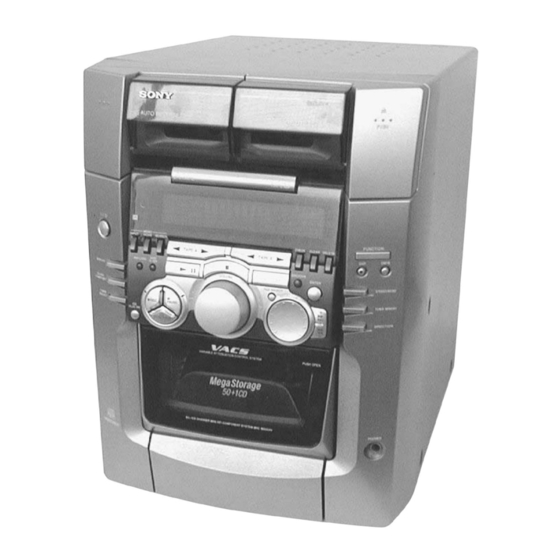
SECTION 1 GENERAL FRONT PANEL 678 90 qaqsqd qfqgqh @/1 button CONTINUE/STEREO/MONO button STANDBY indicator ENTER button MEMO INPUT button PROGRAM/TUNER MEMORY button MEMO SCAN button SHUFFLE/DIRECTION button MEMO SEARCH button + M > button TAPE A h button and indicator . -
Page 7: Rear Panel
REAR PANEL CD DIGITAL OUT connector SUPER WOOFER jack DVD INPUT jack MD/VIDEO INPUT (AUDIO) jack ANTENNA terminal CENTER SPEAKER terminal REAR SPEAKER terminal FRONT SPEAKER terminal AC power cord... - Page 8 This section is extracted from instruction manual.
-
Page 9: Disassembly
SECTION 2 DISASSEMBLY Note : Follow the disassembly procedure in the numerical order given. 2 Three screws (BVTP 3 × 8) 2-1. CASE 3 Case 1 Three screws (CASE3 TP2) 1 Three screws (CASE3 TP2) 2-2. FRONT PANEL SECTION 8 Lug 7 Screws 4 Connector(CN804) (BVTT 3 ×... - Page 10 2-3. DOOR ASSY 1 Two screws (PTPWH 2.6 × 8) 3 Remove the door assy to direction of the arrow A. 2 Open the door assy 2-4. BACK PANEL 7 Eight screws (BVTP 3 × 8) 3 Five screws (BVTP 3 × 8) 2 Connector(CN751) 1 Connector (CN802)
- Page 11 2-5. MAIN BOARD 9 Connector(CN454) 5 Connector(CN454) qa Remove the MAIN board to direction of the arrow. 4 Connector(CN801B) 8 Connector(CN403) 6 Connector(CN461) 3 Connector(CN902) 7 Connector(CN451) 2 Wire (flat type) (9 core) 1 Wire (flat type) (16 core) 0 Two screws (BVTP 3 ×...
- Page 12 2-7. SUB CHASSIS 1 Two screws (BVTT 3 × 8) 3 Sub chassis 2 Three screws (BVTP 3 × 8) 2 Two screws (BVTP 3 × 8) 2-8. CD MECHANISM DECK SECTION 8 Three screws 5 Two screws (BVTT 3 × 10) (BVTT 3 ×...
- Page 13 2-9. CD BASE UNIT 1 Two screws (BTVP 3 × 8) 2 Bracket 3 Two tention springs 5 Base unit 4 Four screws (PTPWH 2.6 × 8) 2-10. BD BOARD, SLED MOTOR (M102) 6 Gear (A) (S) 8 Gear cover 5 Claw 7 Three claws 0 Two screws (P 2 ×...
- Page 14 2-11. OPTICAL PICK-UP 3 Remove the optical pick-up to direction of the arrow A. 2 Sled shaft 1 Claw 2-12. TAPE MECHANISM DECK SECTION 2 Remove the cassette lid (L) assy to direction of the arrow B. 4 Remove the tape mechanism deck section.
- Page 15 2-13. PANEL BOARD 4 Remove the spring (A deck) 3 Remove the cassette lid (L) assy 3 Remove the cassette lid (R) assy 4 Remove the spring (B deck) qa Nine screws qa Five screws (BVTP 2.6 × 8) (BVTP 2.6 × 8) qa Five screws (BVTP 2.6 ×...
- Page 16 2-14. CASSETTE BOARD 4 CASSETTE board 1 Four rivets 3 Two screws (BVTT 2 × 4 (S)) 2 Break the soldering of two flexible flat cables. 2-15. CAPSTAN MOTOR (M1) 4 Remove the capstan motor to direction of the arrow. 3 Remove the belt.
-
Page 17: Test Mode
SECTION 3 TEST MODE [MC Cold Reset] Procedure: The cold reset clears all data including preset data stored in the 1. Press the three buttons x , ENTER and DISPLAY at the RAM to initial conditions. Execute this mode when returning same time. - Page 18 2. The tape A is played back in the FWD mode. After two minutes of the FWD playback, the aging mode advances to the next step. The message: TAPE A AG-2 appears. 3. The tape A runs in fast forward. After two minutes of fast forward, or at the shut-off point, the tape is stopped and the aging mode advances to the next step.
-
Page 19: Mechanical Adjustments
SECTION 4 MECHANICAL ADJUSTMENTS • Torque Measurement • TAPE MECHANISM DECK SECTION Precaution Torque meter Meter reading Mode 1. Clean the following parts with a denatured alcohol-moistened 3.06 N • m to 6.96 N • m swab: CQ-102C 31 to 71 g • cm record/playback heads pinch rollers erase head... - Page 20 PLUS ONE 5. The disc table rotates in the clockwise direction. The disc table rotation time is displayed with “PLUS ONE” slit as a measuring point. 6. Measure the waveform of the oscilloscope when the disc table is rotating. 7. Move the holder (sensor) center so that the flat portion center at the top of the D.SENS (CH1) input waveform and the “H” center of HHOUT (CH2) coincide.
- Page 21 MAGNET ASSY ALIGNMENT 1. Check that there is no disc in the unit and then press the @/1 button to turn ON the power. Open the door, and set a disc in the PLUS ONE slit. 2. Close the door, and while pressing the button, ENTER button and CLOCK/TIMER SET button simultaneously.
-
Page 22: Electrical Adjustments
SECTION 5 ELECTRICAL ADJUSTMENTS 2. Turn the adjustment screw and check output peaks. If the peaks 0 dB = 0.775 V DECK SECTION do not match for L-CH and R-CH, turn the adjustment screw so that outputs match within 1 dB of peak. 1. - Page 23 DECK A/B [MAIN BOARD] (Component Side) Tape Speed Adjustment Note: Start the Tape Speed adjustment as below after setting to the test mode. IC501 Procedure: 1. Press the button to turn ON the power. CN301B 2. Press the button, ENTER button and TIMER SELECT button simultaneously.
-
Page 24: Cd Section
Note : A clear RF signal waveform means that the shape “◊” can be RF PLL Free-run Frequency Check CD SECTION clearly distinguished at the center of the waveform. Procedure : Connect the frequency counter to TP (PLCK) of the BD board. Note : RF signal waveform CD Block is basically designed to operate without adjustment. -
Page 25: Diagrams
HCD-M500AV SECTION 6 DIAGRAMS 6-1. BLOCK DIAGRAM – CD SECTION – OPTICAL PICK-UP BLOCK FOCUS/TRACKING/ (KSM-213BFN/C2NP) SLED/SPINDLE SERVO DIGITAL SIGNAL RF AMP PROCESSOR A+5V IC402 DETECTOR IC101 IC102 • SIGNAL PATH A+5V DIGITAL RF SM EFMI D OUT D IN :DIGITAL OUT FIN 1 EFMO... -
Page 26: Block Diagram - Main Section
HCD-M500AV – MAIN SECTION – IC101 SOUND PROCESSOR SECTION IC141 IC801 CD L RY731 (Page 24) JK801 Q801 FRONT Q141,143 Q145 SPEAKER R CH OVER LOAD MUTE MUTE DET. MAIN SWITCH Q732,733 PB L SECTION Q741-743 LATCH (Page 26) SPEANA POWER DRIVER REC IN L... -
Page 27: Block Diagram - Audio Section
HCD-M500AV – AUDIO SECTION – ANT1 FRONTEND AM/FM IF MPX FM IF TUNER L IF OUT 1 1 FM IF IN L OUT 75Ω CD51 8 FM DET. F OUT SECTION (Page 25) • R-CH is omitted • SIGNAL PATH : FM 16 FM IN ST/MONO... -
Page 28: Circuit Boards Location
6-2. CIRCUIT BOARDS LOCATION THIS NOTE IS COMMON FOR PRINTED WIRING BOARDS AND SCHEMATIC DIAGRAMS. (In addition to this necessary note is printed in each block.) FRONT SP TERM board For schematic diagrams. For printed wiring boards. REAR SP TERM board Note: Note: TRANS board... -
Page 29: Printed Wiring Board - Bd Section
HCD-M500AV 6-3. PRINTED WIRING BOARD – BD SECTION – • See page 27 for Circuit Boards Location. • Semiconductor Location Ref. No. Location BD BOARD D151 IC101 IC102 IC103 M101 IC104 SPINDLE MOTOR Q101 Q102 Q103 (LIMIT) (VC) M102 SLED MOTOR (TE) (RF) -
Page 30: Schematic Diagram - Bd Section
HCD-M500AV 6-4. SCHEMATIC DIAGRAM – BD SECTION – • See page 48 for Waveforms. • See page 48, 50 for IC Pin Functions. KSM-213BFN/C2NP 1SS133T FUNCTION FUNCTION Note: The components identified by mark 0 or dotted line with mark 0 are critical for safety. Replace only with part number specified. -
Page 31: Printed Wiring Board - Cd Motor Section
HCD-M500AV 6-5. PRINTED WIRING BOARD – CD MOTOR SECTION – • See page 27 for Circuit Boards Location. MAIN BOARD CN461 (Page 34) TABLE SENSOR BOARD CD MOTOR BOARD TABLE MOTOR LOADING MOTOR (11) 1-663-974- MAIN BOARD 1-663-971- (11) CN453 (Page 34) MAIN BOARD CN451... -
Page 32: Schematic Diagram - Cd Motor Section
HCD-M500AV 6-6. SCHEMATIC DIAGRAM – CD MOTOR SECTION –... -
Page 33: Printed Wiring Board - Audio Section
HCD-M500AV 6-7. PRINTED WIRING BOARD – AUDIO SECTION – • See page 27 for Circuit Boards Location. MAIN BOARD CN301B (Page34) • Semiconductor CASSETTE BOARD Location Ref. No. Location D361 CN301 D391 IC301 IC361 Q301 IC301 Q303 Q304 Q331 Q332 Q341 Q351 Q352... -
Page 34: Schematic Diagram - Audio Section
HCD-M500AV 6-8. SCHEMATIC DIAGRAM – AUDIO SECTION – • See page 56 for IC Block Diagrams. -
Page 35: Printed Wiring Board - Main Section
HCD-M500AV 6-9. PRINTED WIRING BOARD – MAIN SECTION – • See page 27 for Circuit Boards Location. CASSETTE BOARD REAR AMP BOARD CN301 CN841B (Page32) (Page47) MAIN BOARD • Semiconductor Location Ref. No. Location Ref. No. Location 11 12 Q131 FM75Ω... -
Page 36: Schematic Diagram - Main (1/6) Section
HCD-M500AV 6-10. SCHEMATIC DIAGRAM – MAIN (1/6) SECTION – • See page 48 for Waveforms. • See page 58 for IC Block Diagrams. -
Page 37: Schematic Diagram - Main (2/6) Section
HCD-M500AV 6-11. SCHEMATIC DIAGRAM – MAIN (2/6) SECTION – • See page 32 for Printed Wiring Board. • See page 48 for Waveforms. • See page 52 for IC Pin Functions. • See page 56 for IC Block Diagrams. FUNCTION... -
Page 38: Schematic Diagram - Main (3/6) Section
HCD-M500AV 6-12. SCHEMATIC DIAGRAM – MAIN (3/6) SECTION – • See page 32 for Printed Wiring Board. • See page 57 for IC Block Diagrams. -
Page 39: Schematic Diagram - Main (4/6) Section
HCD-M500AV 6-13. SCHEMATIC DIAGRAM – MAIN (4/6) SECTION – • See page 32 for Printed Wiring Board. • See page 57 for IC Block Diagrams. -
Page 40: Schematic Diagram - Main (5/6) Section
HCD-M500AV 6-14. SCHEMATIC DIAGRAM – MAIN (5/6) SECTION – • See page 32 for Printed Wiring Board. • See page 48 for Waveforms. • See page 53 for IC Pin Functions. FUNCTION... -
Page 41: Schematic Diagram - Main (6/6) Section
HCD-M500AV 6-15. SCHEMATIC DIAGRAM – MAIN (6/6) SECTION – • See page 32 for Printed Wiring Board. -
Page 42: Printed Wiring Board - Power Section
HCD-M500AV 6-16. PRINTED WIRING BOARD – POWER SECTION – • See page 27 for Circuit Boards Location. 6-17. SCHEMATIC DIAGRAM – POWER SECTION – TRANS BOARD T991 POWER TRANSFORMER 1-677-242- (11) REAR AMP FRONT AMP MAIN BOARD BOARD CN903B BOARD CN951 CN901 (Page47) (Page44) -
Page 43: Printed Wiring Board - Panel Section
HCD-M500AV 6-18. PRINTED WIRING BOARD – PANEL SECTION – • See page 27 for Circuit Boards Location. PANEL(R) BOARD PANEL BOARD PANEL(L) BOARD FUNCTION DBFB STEREO/MONO MEMO (CONTINUE) S640 R665 S641 S642 S631 S685 SEARCH SCAN INPUT n TAPE AN S632 S658 TUNER MEMORY... -
Page 44: Schematic Diagram - Panel Section
HCD-M500AV 6-19. SCHEMATIC DIAGRAM – PANEL SECTION – • See page 48 for Waveforms. • See page 56 for IC Block Diagrams. • See page 55 for IC Pin Functions. FUNCTION... -
Page 45: Printed Wiring Board - Front Amp Section
HCD-M500AV 6-20. PRINTED WIRING BOARD – FRONT AMP SECTION – • See page 27 for Circuit Boards Location. TRANS BOARD CN992 (Page41) FRONT AMP BOARD • Semiconductor Location PHONES BOARD Ref. No. Location D731 D732 HP803 D733 PHONES D751 D752 D801 D802 D803... -
Page 46: Schematic Diagram - Front Amp Section
HCD-M500AV 6-21. SCHEMATIC DIAGRAM – FRONT AMP SECTION –... -
Page 47: Schematic Diagram - Rear Amp Section
HCD-M500AV 6-22. SCHEMATIC DIAGRAM – REAR AMP SECTION –... -
Page 48: Printed Wiring Board - Rear Amp Section
HCD-M500AV 6-23. PRINTED WIRING BOARD – REAR AMP SECTION – • See page 27 for Circuit Boards Location. REAR SP TERM BOARD REAR AMP BOARD • Semiconductor Location Ref. No. Location CENTER SPEAKER D771 D841 D842 D881 D882 D883 REAR SPEAKER D961 MAIN BOARD IC831... -
Page 49: Waveforms
6-24. WAVEFORMS 6-25. IC PIN FUNCTION DESCRIPTION BD BOARD IC101 LA9240M (FOCUS/TRACKING/SLED SERVO, RF AMP) – MAIN Section – – PANEL Section – Pin No. Pin Name Function Connected to the pick-up photodiode FIN2 IC2 ws (XOUT) IC501 ea (EXTAL) IC601 8 (X-OUT) Added with FIN1 to create RF signal, subtracted with FIN1 to create FE signal FIN1... - Page 50 Pin No. Pin Name Function SLOF Sled servo off control input CV– CLV error signal is input from the digital signal processor CLV error signal is input from the digital signal processor RFSM RF output Works together with the RFSM pin to set the RF gain and the 3T compensation constant for RFS–...
- Page 51 BD BOARD IC102 LC78622E (DIGITAL SIGNAL PROCESSOR) Pin No. Pin Name Function DEFI Defect detection signal (DEF) input (Be sure to connect to 0 when not in use) PLL test input to incorporates a pull-down resistor (Be sure to connect to 0V) PLL phase comparison output for external VCO control VVSS —...
- Page 52 Pin No. Pin Name Function EMPH Deemphasis monitor The deemphasis disc is being played back when “H” C2 flag output DOUT Digital OUT output (EIAJ format) TEST3 Test input Incorporates a pull-down resistor Be sure to connect to 0V TEST4 Test input Incorporates a pull-down resistor Be sure to connect to 0V —...
- Page 53 MAIN BOARD IC401 CXP84632-158Q (CD CHANGER CONTROL) Pin No. Pin Name Function — — Not used ICSW IC reset signal output — — Not used HHOUT Plus one LED signal output — — Not used 6 to 13 D0 to D7 SRAM data I/O 14 to 28 A0 to A14...
- Page 54 MAIN BOARD IC501 CXP84632-159Q (MASTER CONTROL) Pin No. Pin Name Function TDA DATA Data signal output for IC101 — Not used — Not used — Not used NC (VSS) — Not used (Ground) PB MUTE TC PB mute control signal output REC MUTE TC REC mute control signal output PB A/B...
- Page 55 Pin No. Pin Name Function STEREO Stereo detection for tuner TUNED Tuned detection for tuner — Not used NC (VSS) — Not used (Connect to ground) NC (VSS) — Not used (Connect to ground) NC (VSS) — Not used (Connect to ground) Not used (Connect to ground) NC (VSS) —...
- Page 56 PANEL BOARD IC601 TMP87CM74AF-1G57 (DISPLAY CONTROL) Pin No. Pin Name Function 1 to 6 LED3 to LED8 LED driver output — Ground XOUT X’tal (8MHz) X’tal (8MHz) RESET Reset signal input 11, 12 LED9, LED10 LED driver output TEST — Not used 14 to 18 LED11 to LED15...
-
Page 57: Ic Block Diagrams
6-26. IC BLOCK DIAGRAMS IC603 (PANEL BOARD) BA3833F-E2 IC461 (MAIN BOARD) BA6780 RESET RESET 18 RESET VIN1 VIN2 REFFERENCE PREF 17 f01 CURRENT FIN1 FIN2 LINE 16 f02 LINE RIN1 RIN2 15 f03 IOUT BIAS 13 f Bias VREF 12 VCC FBIN- VREG 11 NC... - Page 58 IC101 (MAIN BOARD) TDA7440D 17 16 SUPPLY VREF SPKR ATT TREBLE VOLUME BASS LEFT 0/30dB I2CBUS DECODER LATCHES 2dB STEP SPKR ATT INPUT MULTIPLEXER TREBLE BASS VOLUME RIGHT GAIN 1 2 3 4 IC201 (MAIN BOARD) M62464FP 56 55 MODIFIED DUAL TIME CONSTANT FULL WAVE B-TYPE...
- Page 59 IC1 (MAIN BOARD) LA1833N RF.AM DECODER BUFF ANTI-BIRDIE PILOT CANCEL STEREO P-DET Ø LEVEL AM/FM COMP PILOT 19k<0 19k<π/2 304kHz S-CURVE TUNING DRIVE IC2 (MAIN BOARD) LC72136 14 13 REFERENCE DIVIDER DATA SHIFT REGISTER LATCH 10 11...
-
Page 60: Exploded Views
SECTION 7 EXPLODED VIEWS NOTE: • -XX, -X mean standardized parts, so they may • The mechanical parts with no reference number The components identified by mark 0 or have some differences from the original one. in the exploded views are not supplied. dotted line with mark 0 are critical for safety. - Page 61 1-677-243-11 CD DOOR BOARD 4-230-343-01 KNOB (VOLUME) 4-989-312-01 LATCH, NS 4-230-342-01 KNOB (SELECTOR) 3-354-963-01 DAMPER 4-962-708-52 EMBLEM (4-A), SONY 4-957-577-31 SCREW PTP WH (2.6X8) (DIA. 10) 4-230-341-01 DECORATION PANEL 1-677-245-11 PHONE BOARD A-4412-482-A WINDOW (L) ASSY, CASSET 4-230-348-01 SPRING (DOOR2) TORSION...
- Page 62 7-3. CHASSIS SECTION not supplied supplied T991 T992 CD MECHANISM DECK SECTION-1 not supplied CD MECHANISM DECK SECTION-2 not supplied not supplied The components identified by mark 0 or dotted line with mark 0 are critical for safety. Replace only with part number specified. Ref.
- Page 63 7-4. MECHANISM DECK SECTION-1 (CDM46B1) OPTICAL PICK-UP SECTION not supplied Ref. No. Part No. Description Remarks Ref. No. Part No. Description Remarks * 301 1-663-975-11 SW BOARD * 314 4-988-454-01 COVER (LEVER) * 302 4-988-427-01 COVER, CAM * 315 4-988-421-01 HOLDER (MAGNET) 4-988-420-01 SLIDER (LOADING) A-4672-522-A MAGNET ASSY 4-988-436-01 SPRING (LOADING), TORSION...
- Page 64 7-5. MECHANISM DECK SECTION-2 (CDM-46B1) Ref. No. Part No. Description Remarks Ref. No. Part No. Description Remarks * 351 1-663-971-11 TABLE SENSOR BOARD * 357 4-988-426-01 BASE (CDM) 4-988-414-01 BELT * 358 1-663-972-11 DISC SENSOR (R) BOARD 4-988-423-01 GEAR (A) (LOADING) * 359 1-663-974-11 CD MOTOR BOARD 4-988-425-01 PULLEY...
- Page 65 7-6. OPTICAL PICK UP SECTION (KSM-213BFN/C2NP) not supplied M102 M101 The components identified by mark 0 or dotted line with mark 0 are critical for safety. Replace only with part number specified. Ref. No. Part No. Description Remarks Ref. No. Part No.
- Page 66 7-7. TAPE MECHANISM DECK SECTION (TCM-230AWR21) not supplied not supplied not supplied not supplied not supplied not supplied Ref. No. Part No. Description Remarks Ref. No. Part No. Description Remarks X-3374-156-4 PINCH LEVER (REV) ASSY 4-227-239-01 BELT (CAPSTAN C) X-3374-155-4 PINCH LEVER (FWD) ASSY A-2100-912-A TODECK (TCM-230AWR21) 3-019-208-01 WASHER, STOPPER A-4475-079-A CASSETTE BOARD, COMPLETE...
-
Page 67: Electrical Parts List
SECTION 8 ELECTRICAL PARTS LIST NOTE: Ref. No. Part No. Description Remarks Ref. No. Part No. Description Remarks • Due to standardization, replacements in the • RESISTORS When indicating parts by reference number, parts list may be different from the parts All resistors are in ohms. - Page 68 CASSETTE Ref. No. Part No. Description Remarks Ref. No. Part No. Description Remarks 1-216-295-91 SHORT R162 1-216-037-00 METAL CHIP 1/10W JW10 1-216-295-91 SHORT R163 1-216-049-91 RES-CHIP 1/10W R164 1-216-065-91 RES-CHIP 4.7K 1/10W < TRANSISTOR > R165 1-216-025-91 RES-CHIP 1/10W R166 1-216-025-91 RES-CHIP 1/10W Q101...
- Page 69 CASSETTE CD DOOR CD LED Ref. No. Part No. Description Remarks Ref. No. Part No. Description Remarks C346 1-163-009-11 CERAMIC CHIP 0.001uF R327 1-216-077-91 RES-CHIP 1/10W C347 1-130-479-00 MYLAR 0.0047uF 5% R328 1-216-077-91 RES-CHIP 1/10W C348 1-136-293-11 MYLAR 0.0082uF 5.00% 50V R331 1-216-073-00 METAL CHIP 1/10W...
- Page 70 CD LED CD MOTOR DISC SENSOR (R) DISC SENSOR (S) DOOR LED FRONT AMP Ref. No. Part No. Description Remarks Ref. No. Part No. Description Remarks < RESISTOR > C801 1-128-582-11 ELECT 10uF 20.00% 100V C802 1-128-582-11 ELECT 10uF 20.00% 100V R691 1-249-402-11 CARBON 1/4W F...
- Page 71 FRONT AMP FRONT SP TERM MAIN Ref. No. Part No. Description Remarks Ref. No. Part No. Description Remarks R702 1-216-089-91 RES-CHIP 1/10W < RELAY > R704 1-216-089-91 RES-CHIP 1/10W R705 1-216-073-00 METAL CHIP 1/10W RY731 1-515-920-11 RELAY (24V) R706 1-216-089-91 RES-CHIP 1/10W R707 1-216-073-00 METAL CHIP...
- Page 72 MAIN Ref. No. Part No. Description Remarks Ref. No. Part No. Description Remarks 1-126-964-11 ELECT 10uF 20.00% 50V C150 1-126-961-11 ELECT 2.2uF 20.00% 50V 1-126-963-11 ELECT 4.7uF 20.00% 50V C156 1-126-934-11 ELECT 220uF 20.00% 10V 1-162-294-31 CERAMIC 0.001uF C157 1-126-933-11 ELECT 100uF 20.00% 16V 1-162-851-11 CERAMIC...
- Page 73 MAIN Ref. No. Part No. Description Remarks Ref. No. Part No. Description Remarks C251 1-126-964-11 ELECT 10uF 20.00% 50V C481 1-126-963-11 ELECT 4.7uF 20.00% 50V C252 1-162-282-31 CERAMIC 100PF C482 1-126-963-11 ELECT 4.7uF 20.00% 50V C253 1-126-964-11 ELECT 10uF 20.00% 50V C501 1-104-664-11 ELECT 47uF...
- Page 74 MAIN Ref. No. Part No. Description Remarks Ref. No. Part No. Description Remarks D141 8-719-921-40 DIODE MTZJ-T-72-4.7C < JACK > D142 8-719-911-19 DIODE 1SS133T-72 D143 8-719-911-19 DIODE 1SS133T-72 J101 1-794-634-11 JACK, PIN 2P D172 8-719-911-19 DIODE 1SS133T-72 J103 1-794-635-11 JACK, PIN 1P D176 8-719-911-19 DIODE 1SS133T-72 J201...
- Page 75 MAIN Ref. No. Part No. Description Remarks Ref. No. Part No. Description Remarks Q922 8-729-620-05 TRANSISTOR 2SC2603TP-EF R146 1-249-419-11 CARBON 1.5K 1/4W F Q931 8-729-993-43 TRANSISTOR 2SA934R R147 1-249-429-11 CARBON 1/4W Q971 8-729-209-15 TRANSISTOR 2SD2012 R148 1-249-429-11 CARBON 1/4W Q972 8-729-119-78 TRANSISTOR 2SC1740S-QRT R149 1-247-895-00 CARBON...
- Page 76 MAIN PANEL Ref. No. Part No. Description Remarks Ref. No. Part No. Description Remarks R222 1-247-883-00 CARBON 150K 1/4W R522 1-247-807-31 CARBON 1/4W R223 1-249-437-11 CARBON 1/4W R523 1-247-807-31 CARBON 1/4W R224 1-247-876-11 CARBON 1/4W R524 1-247-807-31 CARBON 1/4W R225 1-249-437-11 CARBON 1/4W R525...
- Page 77 PANEL Ref. No. Part No. Description Remarks Ref. No. Part No. Description Remarks < CAPACITOR > D665 8-719-080-73 DIODE L-1154GD(n TAPE A) C601 1-124-584-00 ELECT 100uF < FERRITE BEAD > C602 1-165-319-11 CERAMIC CHIP 0.1uF C603 1-126-157-11 ELECT 10uF FB601 1-500-242-22 FERRITE C604 1-165-319-11 CERAMIC CHIP...
- Page 78 PANEL PANEL L PANEL R PHONE REAR AMP Ref. No. Part No. Description Remarks Ref. No. Part No. Description Remarks R642 1-216-065-91 RES-CHIP 4.7K 1/10W 1-677-239-11 PANEL L BOARD R643 1-216-029-00 METAL CHIP 1/10W ************** R644 1-216-029-00 METAL CHIP 1/10W R645 1-216-033-00 METAL CHIP 1/10W...
- Page 79 REAR AMP Ref. No. Part No. Description Remarks Ref. No. Part No. Description Remarks C843 1-163-005-11 CERAMIC CHIP 470PF < RESISTOR > C844 1-163-005-11 CERAMIC CHIP 470PF C845 1-163-001-11 CERAMIC CHIP 220PF R257 1-216-049-91 RES-CHIP 1/10W C846 1-163-001-11 CERAMIC CHIP 220PF R258 1-216-049-91 RES-CHIP...
- Page 80 REAR AMP REAR SP TERM SUB TRANS TABLE SENSOR TRANS Ref. No. Part No. Description Remarks Ref. No. Part No. Description Remarks R897 1-220-755-11 METAL 0.22 1-663-975-11 SW BOARD ********** < RELAY > < CONNECTOR > RY771 1-515-920-11 RELAY (24V) RY772 1-515-920-11 RELAY (24V) * CN54...
- Page 81 HCD-M500AV Remarks Ref. No. Part No. Description Remarks Ref. No. Part No. Description MISCELLANEOUS *************** 1-757-074-11 WIRE (FLAT TYPE) (12 CORE) 1-773-055-11 WIRE (FLAT TYPE) (17 CORE) 1-757-073-11 WIRE (FLAT TYPE) (10 CORE) 1-783-531-11 CORD, POWER 1-782-558-21 WIRE (FLAT TYPE) (16 CORE) 1-769-920-11 WIRE (FLAT TYPE) (9 CORE) 1-777-874-11 WIRE (FLAT TYPE) (16 CORE) 8-820-026-03 OPTICAL PICK-UP KSM-213BFN/C2NP...
- Page 82 HCD-M500AV MEMO...
- Page 83 HCD-M500AV REVISION HISTORY Clicking the version allows you to jump to the revised page. Also, clicking the version at the upper right on the revised page allows you to jump to the next revised page. Ver. Date Description of Revision 2001.07 Correction of exploded views (66, 69, 70).
- Page 84 SS-M100/M500AV SERVICE MANUAL US Model This set is the speaker system in MHC-M100/M300AV/M500AV. Photo: SS-M500AV MHC-M100 MHC-M300/M500AV SPEAKER SYSTEM SS-M100 SS-M500AV SPECIFICATIONS SS-M100 SS-M500AV Speaker system 3-way, bass-reflex type Speaker system 3-way, bass-reflex type Speaker units magnetically shielded type Woofer:...
- Page 85 4-874-614-61 SCREW (4) (3.5X16) TAPPING 1-529-818-11 SPEAKER (16cm) (M100) 1-529-820-11 SPEAKER (16cm) (M500AV) A-4412-527-A CABINET ASSY, SPEAKER (M100) A-4412-529-A CABINET ASSY, SPEAKER (M500AV) Sony Corporation 9-929-280-11 2000E091613-1D Audio Entertainment Group Printed in Japan © 2000. 5 Published by HA Quality Assurance Dept.
- Page 86 SS-CT175/CT175D/RC175/ RC175D/RS175/RS175D SERVICE MANUAL US Model This set is the speaker system in MHC-M300AV/M500AV. Photo: SS-CT175D Photo: SS-RS175D SS-RC175/RC175D is composed for following model. COMPONENT MODEL NAME FOR SS-RC175/RC175D MHC-M300AV MHC-M500AV SS-RC175 SS-RC175D SPEAKER SYSTEM SS-CT175 CENTER SPEAKER SS-CT175D SS-RS175 REAR SPEAKER SS-RS175D SPECIFICATIONS...
- Page 87 4-230-780-01 CABINET 7-685-663-79 SCREW +BVTP 4X16 TYPE2 N-S ******************************** 1-769-433-12 CORD, SPEAKER (10m) 1-694-742-11 TERMINAL BOARD (2P) 1-529-821-11 SPEAKER (8cm) (SS-RS175) Sony Corporation 9-929-281-11 2000E091613-1D Audio Entertainment Group Printed in Japan © 2000. 5 Published by HA Quality Assurance Dept.
- Page 88 KNOB (A), PUSH 4-226-228-01 KNOB (VOL) 4-226-228-11 KNOB (VOL) A-4411-960-A CABINET ASSY, SPEAKER A-4412-288-A CABINET ASSY, SPEAKER 4-227-118-31 PANEL, REAR 4-229-176-01 PANEL, REAR SUBWOOFER SYSTEM 2000E001613-1D Sony Corporation Printed in Japan ©2000.5 Published by HA Quality Assurance Dept. Audio Entertainment Group 9-929-282-11...