Table of Contents
Advertisement
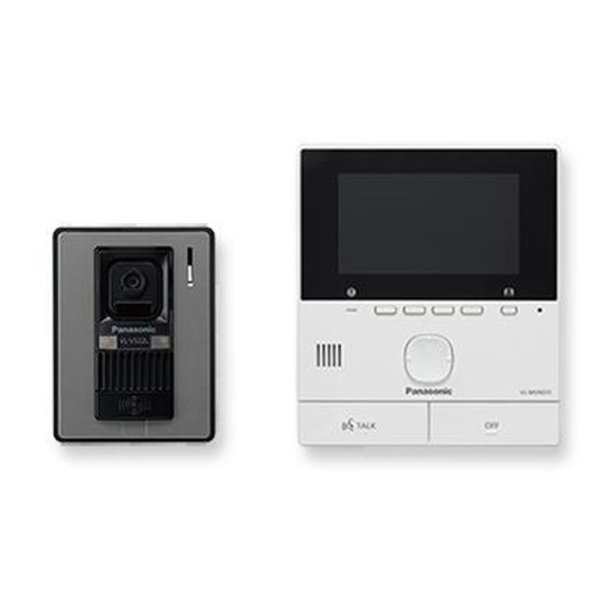
Video Intercom System
VL-SVN511BX
Model No.
VL-MVN511BX
VL-V522LCE
VL-RLY1
VL-PS241
VL-SVN511CX
Model No.
VL-SVN511CX1
Model No.
VL-MVN511BX
VL-V522LCE
VL-RLY1
VL-PS241
(BX: for Asia, Middle Near East and Africa)
(CX: for Middle East and Hong Kong)
(CX1: for UAE)
© Panasonic Corporation 2019
Unauthorized copying and distribution is a violation
of law.
ORDER NO. KMA1511067CE
[Version 2.0]
Advertisement
Table of Contents

Related Manuals for Panasonic VL-SVN511BX


Summary of Contents for Panasonic VL-SVN511BX
- Page 1 VL-SVN511CX1 Model No. VL-MVN511BX VL-V522LCE VL-RLY1 VL-PS241 (BX: for Asia, Middle Near East and Africa) (CX: for Middle East and Hong Kong) (CX1: for UAE) [Version 2.0] © Panasonic Corporation 2019 Unauthorized copying and distribution is a violation of law.
-
Page 2: Table Of Contents
VL-SVN511BX/VL-SVN511CX/VL-SVN511CX1 TABLE OF CONTENTS PAGE PAGE 1 Safety Precautions -----------------------------------------------4 6 Installation Instructions -------------------------------------- 18 1.1. Safety Precautions-----------------------------------------4 7 Operating Instructions---------------------------------------- 18 1.2. For Service Technicians ----------------------------------4 8 Troubleshooting Guide --------------------------------------- 19 1.3. Power Caution ----------------------------------------------4 8.1. Operation Check of the Door Station --------------- 19 2 Warning --------------------------------------------------------------5 8.2. - Page 3 VL-SVN511BX/VL-SVN511CX/VL-SVN511CX1 9.2.6. Item to be checked after completion of 16 Change Information -------------------------------------------- 88 assembly (camera lens angle adjustment) ----42 9.3. Power Supply Unit----------------------------------------43 9.4. Relay Box---------------------------------------------------44 10 Measurements and Adjustments---------------------------45 10.1. Main Monitor Station -------------------------------------45 10.1.1. Connections-------------------------------------------45 10.1.2. Things to do after replacing IC -------------------46 10.1.3.
-
Page 4: Safety Precautions
VL-SVN511BX/VL-SVN511CX/VL-SVN511CX1 1 Safety Precautions 1.1. Safety Precautions 1. Before servicing, unplug the power cord to prevent an electrical shock. 2. When replacing parts, use only manufacturer’s recommended components for safety. 3. Check the condition of power cord. Replace if wear or damage is evident. -
Page 5: Warning
VL-SVN511BX/VL-SVN511CX/VL-SVN511CX1 2 Warning 2.1. About Lead Free Solder (PbF: Pb free) Note: In the information below, Pb, the symbol for lead in the periodic table of elements, will refer to standard solder or solder that con- tains lead. We will use PbF solder when discussing the lead free solder used in our manufacturing process which is made from Tin, (Sn), Silver, (Ag), and Copper, (Cu). -
Page 6: Insulation Resistance Test
VL-SVN511BX/VL-SVN511CX/VL-SVN511CX1 2.2. Insulation Resistance Test 1. Unplug the AC power cord and short the two prongs of the plug with a jumper wire. 2. Measure the resistance value with ohmmeter between the jumpered AC plug and all the terminals as shown in following figures. -
Page 7: Specifications
VL-SVN511BX/VL-SVN511CX/VL-SVN511CX1 3 Specifications Design and specifications are subject to change without notice. 3.1. Main monitor station (VL-MVN511) Power source: Power supply unit (VL-PS241) 24 V DC, 0.5 A Power consumption: Standby: Approx. 1.8 W During operation: Approx. 10 W Dimensions (mm): Approx. -
Page 8: Door Station (Vl-V522Lce)
VL-SVN511BX/VL-SVN511CX/VL-SVN511CX1 3.4. Door station (VL-V522LCE) Power source: Power supplied by the main monitor Dimensions (mm): Approx. 131 x 99 x 36.5 (Excluding protruding sections) (height x width x depth) Mass (Weight): Approx. 200 g Operating environment: Ambient temperature: Approx. -15 °C to +55 °C... -
Page 9: Technical Descriptions
VL-SVN511BX/VL-SVN511CX/VL-SVN511CX1 4 Technical Descriptions 4.1. What is a Video Intercom? 4.2. Video Intercom 4.2.1. Block Diagram Here is the block diagram of Video intercom system in Fig 1.1. The image data is converted into NTSC signal by Camera Unit. The NTSC signal is modulated into FM, then transferred to the Monitor station through the interphone cable. -
Page 10: Cmos Image Sensor Unit Block
VL-SVN511BX/VL-SVN511CX/VL-SVN511CX1 4.2.2. Cmos Image Sensor Unit Block Cmos image sensor unit and DSP blocks are shown in Fig. 1.2. Basically the image through the lens is converted into the elec- tric signal by the optical filter and cmos image sensor. Then it is transferred to the DSP block. -
Page 11: Voice
VL-SVN511BX/VL-SVN511CX/VL-SVN511CX1 4.2.7. Voice The voice from the microphone of Door station is amplified and sent to the Monitor station through 2-4 wire conversion circuit, DC blocking capacitor, transformer and interphone cable. The visitor’s voice is passed through the separation transformer, DC blocking capacitor, 2-4 wire conversion circuit and amplifier, and the voice can be heard through the speaker of the Monitor station. -
Page 12: Ic Operation
VL-SVN511BX/VL-SVN511CX/VL-SVN511CX1 4.3. IC Operation 4.3.1. Monitor Station Section 4.3.1.1. Main Monitor station Diagram Analog image signal process Camera power supply IC670 Door Door Phone I/F Image station ×2 Digital signal process (Image Control) IC100 5"WQVGA LCD panel DPJP3 Key/LCD External Sensor... - Page 13 VL-SVN511BX/VL-SVN511CX/VL-SVN511CX1 4.3.1.2. Power Supply Unit (VL-PS241) Power control IC (IC1) Input voltage: AC 220V~240V Output voltage: DC 24V Package: 7pin DIP Outline of Operation: It generate from AC 220V~240V to DC 24V. 4.3.1.3. Power Board (VL-MVN511) Regulator for Power 12V (IC30)
- Page 14 VL-SVN511BX/VL-SVN511CX/VL-SVN511CX1 4.3.1.4.2. Audio Part Sub CPU (IC405) 8M FROM (IC402) Operating Power Supply: +3.3V Operating Power Supply: +1.8V Operating Power Supply: +4V (SP AMP) Package: 8pin SOIC Operating Power Supply: +3.2V (RF) Memory capacity: 8Mbit Operating Power Supply: +1.8V (Core) Outline of Operation: Storing the program of IC405.
-
Page 15: Door Station Section
VL-SVN511BX/VL-SVN511CX/VL-SVN511CX1 4.3.2. Door Station Section 4.3.2.1. Door station Diagram... - Page 16 VL-SVN511BX/VL-SVN511CX/VL-SVN511CX1 4.3.2.2. Main Board Call Button (SW301) Outline of Operation : When a visitor presses the Call Button, a chime tone will ring at the monitor station. FM Signal Modulator (IC200) Operating Power Supply : +5V (+5V : 2, 9pin) Package : 24pin SOP Outline of Operation : The frequency modulation of the video signal taken in from Camera Unit is carried out.
-
Page 17: Relay Box Section
VL-SVN511BX/VL-SVN511CX/VL-SVN511CX1 4.3.3. Relay box Section 4.3.3.1. Relay box Diagram Electric lock 1 Relay terminal terminal Electric lock 2 Relay terminal VL-SVN511 / VL-RLY1 : Relay box diagram... -
Page 18: Location Of Controls And Components
VL-SVN511BX/VL-SVN511CX/VL-SVN511CX1 5 Location of Controls and Components Refer to the Operating Instructions. Note: You can download and refer to the Operating Instructions (Instruction book) on TSN Server. 6 Installation Instructions Refer to the Operating Instructions. Note: You can download and refer to the Installation Guide on TSN Server. -
Page 19: Troubleshooting Guide
VL-SVN511BX/VL-SVN511CX/VL-SVN511CX1 8 Troubleshooting Guide 8.1. Operation Check of the Door Station Reference: • Refer to Calling Operation in Signal Route (P.32). • Refer to Talk Signal in Signal Route (P.32). - Page 20 VL-SVN511BX/VL-SVN511CX/VL-SVN511CX1 Reference: • Refer to Image Signal in Signal Route (P.32).
- Page 21 VL-SVN511BX/VL-SVN511CX/VL-SVN511CX1 Reference: • Refer to AM Signal in Signal Route (P.32).
-
Page 22: Operation Check Of The Main Monitor Station
VL-SVN511BX/VL-SVN511CX/VL-SVN511CX1 8.2. Operation Check of the Main Monitor Station Reference: (*1) Defect of the Main Monitor Station Power Supply(P.23). (*2) Defect of the WiFi Communication (P.26). (*3) Operation Check of the Door Station(P.19). (*4) Defect of the Communication between the Main Monitor Station and the Door Station(P.28). -
Page 23: Defect Of The Main Monitor Station Power Supply
VL-SVN511BX/VL-SVN511CX/VL-SVN511CX1 8.2.1. Defect of the Main Monitor Station Power Supply... - Page 24 VL-SVN511BX/VL-SVN511CX/VL-SVN511CX1 [Defect of the Main unit power supply]...
- Page 25 VL-SVN511BX/VL-SVN511CX/VL-SVN511CX1...
-
Page 26: Defect Of The Wifi Communication
VL-SVN511BX/VL-SVN511CX/VL-SVN511CX1 Reference: • Refer to LCD start up in Signal Route (P.32). 8.2.2. Defect of the WiFi Communication Reference: • Refer to [Defect of the Main unit power supply] (P.24). -
Page 27: Defect Of The Main Monitor Station Video Recording
VL-SVN511BX/VL-SVN511CX/VL-SVN511CX1 8.2.3. Defect of the Main Monitor Station Video Recording Reference: • Refer to Recording Image Operation in Signal Route (P.32). -
Page 28: Defect Of The Communication Between The Main Monitor Station And The Door Station
VL-SVN511BX/VL-SVN511CX/VL-SVN511CX1 8.2.4. Defect of the Communication between the Main Monitor Station and the Door Sta- tion Reference: • Refer to Talk Signal in Signal Route (P.32). • Refer to Image Signal in Signal Route (P.32). • (*1) How to Remove the Main Board, Mic Board, Speaker and LCD [No.3] (P.36). -
Page 29: Defect Of The Communication Between The Door Station And The Pbx
VL-SVN511BX/VL-SVN511CX/VL-SVN511CX1 8.2.5. Defect of the Communication between the Door Station and the PBX Reference: • (*1) How to Remove the Main Board, Mic Board, Speaker and LCD [No.3] (P.36). • (*3) Operation Check of the Door Station (P.19). • (*6) Operation Check of the Main Monitor Station (P.22). -
Page 30: Defect Of The Operation Of The Electric Lock
VL-SVN511BX/VL-SVN511CX/VL-SVN511CX1 8.2.6. Defect of the operation of the electric lock Reference: • Refer to [Defect of the Main unit power supply] (P.24). • (*1) How to Remove the Main Board, Mic Board, Speaker and LCD [No.3] (P.36). 8.2.7. Defect of the external input Reference: •... -
Page 31: Error Messages
VL-SVN511BX/VL-SVN511CX/VL-SVN511CX1 8.3. Error Messages Refer to Operating Instructions for the settings. Main monitor station Display Cause & Solution IP address is duplicated. • The same IP address of the main monitor is used by another device. Confirm the current IP address of the main monitor, and then reconfigure it so that is does not overlap with other IP addresses. -
Page 32: Signal Route
VL-SVN511BX/VL-SVN511CX/VL-SVN511CX1 8.4. Signal Route This chapter provides the testing procedures required for the P.C.B. parts. A signal route to be tested is determined depending upon purposes. The signal mainly flowing on this route is analog. You can trace the signal with an oscilloscope. The signal flow on each route is shown in the Check Sheet here. - Page 33 VL-SVN511BX/VL-SVN511CX/VL-SVN511CX1...
- Page 34 VL-SVN511BX/VL-SVN511CX/VL-SVN511CX1...
-
Page 35: Disassembly And Assembly Instructions
VL-SVN511BX/VL-SVN511CX/VL-SVN511CX1 9 Disassembly and Assembly Instructions 9.1. Main Monitor Station 9.1.1. How to Remove the DC cable [No.1] Procedure No.1 1. Remove a screw ① . 2. Remove the DC cord cover. 3. Loosen screws and pull out the wires of the DC cable from the terminal connectors. -
Page 36: How To Remove The Main Board, Mic Board, Speaker And Lcd [No.3]
VL-SVN511BX/VL-SVN511CX/VL-SVN511CX1 9.1.3. How to Remove the Main Board, Mic Board, Speaker and LCD [No.3] Procedure No.1No.2No.3 1. Remove 2 screws ① . 2. Remove the solder of the Mic Board lead wire (Fig.1). 3. Remove the solder of the Speaker lead wire (Fig.3). -
Page 37: Door Station
VL-SVN511BX/VL-SVN511CX/VL-SVN511CX1 9.2. Door Station 9.2.1. How to Remove the Mounting Base [No.1] Procedure No.1 1. Open the screw cover, as shown in Fig. F. 2. Loose 1 screw (D). 3. Remove the Mounting base, as shown in Fig. G. -
Page 38: How To Remove The Main Board And Camera Unit [No.2]
VL-SVN511BX/VL-SVN511CX/VL-SVN511CX1 9.2.2. How to Remove the Main Board and Camera Unit [No.2] Procedure No.1No.2 1. Remove 2 screws (E). 2. Please remove the cabinet cover from cabinet body with care to the tabs. 3. Remove the solder on the lead wire-A and lead wire-B. -
Page 39: How To Remove The Mic Board And Speaker [No.3]
VL-SVN511BX/VL-SVN511CX/VL-SVN511CX1 9.2.3. How to Remove the Mic Board and Speaker [No.3] Procedure No.1No.2No.3 1. Remove the Mic board. 2. Remove 2 screws (F). 3. Remove the Speaker. - Page 40 VL-SVN511BX/VL-SVN511CX/VL-SVN511CX1 9.2.3.1. Note for Microphone Assembly (for anti-feedback)
-
Page 41: How To Remove The Front Panel [No.4]
VL-SVN511BX/VL-SVN511CX/VL-SVN511CX1 9.2.4. How to Remove the Front Panel [No.4] Procedure No.4 1. After unhook the 6 tabs as shown in Fig. J, remove the Front panel. -
Page 42: Installation Of The Lead Wires
VL-SVN511BX/VL-SVN511CX/VL-SVN511CX1 9.2.5. Installation of the lead wires When assembling the door station, route the lead wires as shown in the figure below, and be careful that they do not get caught. 9.2.6. Item to be checked after completion of assembly (camera lens angle adjustment) After completing assembly work, move the angle adjustment lever on the rear surface in the left and right directions, and confirm that it moves all the way. -
Page 43: Power Supply Unit
VL-SVN511BX/VL-SVN511CX/VL-SVN511CX1 9.3. Power Supply Unit 1. Remove 4 screws ① . 2. Remove the Power Board by unhooking 2 tabs. -
Page 44: Relay Box
VL-SVN511BX/VL-SVN511CX/VL-SVN511CX1 9.4. Relay Box 1. Remove 4 screws ① . 2. Remove the Cabinet and Relay Board. -
Page 45: Measurements And Adjustments
VL-SVN511BX/VL-SVN511CX/VL-SVN511CX1 10 Measurements and Adjustments 10.1. Main Monitor Station 10.1.1. Connections When replacing the main board (Monitor Station), please refer to the following items for adjusting. -
Page 46: Things To Do After Replacing
VL-SVN511BX/VL-SVN511CX/VL-SVN511CX1 10.1.2. Things to do after replacing IC If repairing FLASH Memory, EEPROM, it is necessary to initialize and adjustment. The set doesn't operate if it is not executed. -
Page 47: When Replacing Bbic And X'tal
VL-SVN511BX/VL-SVN511CX/VL-SVN511CX1 10.1.3. When replacing BBIC and X'tal Preparation: 1. PC setting refer to “Things to do after replacing IC (P.46). 2. Supply AC 230V to Power supply unit (PS241). Note: Test points: Refer to Main Board (Bottom View) (P.63). -
Page 48: Factory Mode
VL-SVN511BX/VL-SVN511CX/VL-SVN511CX1 10.1.4. Factory Mode Entering Factory Mode: 1. Turn AC Power “ON”, while pressing [OFF] button, [TALK] button and [F4] at the same time, about 5 seconds or more. (FACTORY MODE screen is displayed.) In order to exit Factory Mode:... - Page 49 VL-SVN511BX/VL-SVN511CX/VL-SVN511CX1 10.1.4.1. Factory Setup Initialize the logs and the all parameters except for the factory adjusted value, and delete the recorded images. 1. Select “FACTORY SETUP” by Navigation key. 2. Press [F4 (DECIDE)]. 3. Press [F4 (RUN)]. • If “WiFi module starting ...” is displayed, wait until disap- pear.
- Page 50 VL-SVN511BX/VL-SVN511CX/VL-SVN511CX1 10.1.4.2. White Balance Adjustment The adjustment is done only when the color of the LCD display has changed after you have replaced the LCD. (Basically, adjustment is unnecessary.) 1. Select “TECHNICAL MODE 1” by Navigation key. 2. Select “WHITE BALANCE” by Navigation key.
- Page 51 VL-SVN511BX/VL-SVN511CX/VL-SVN511CX1 10.1.4.3. Advance settings Mode This setting is optional settings for e-mail transmission. Entering Advance settings Mode: 1. Turn AC Power “ON”, while pressing [OFF] button, [TALK] button and [F1] at the same time, about 5 seconds or more.
-
Page 52: Miscellaneous
VL-SVN511BX/VL-SVN511CX/VL-SVN511CX1 11 Miscellaneous 11.1. How to Replace the Flat Package IC Even if you do not have the special tools (for example, a spot heater) to remove the Flat IC, with some solder (large amount), a soldering iron and a cutter knife, you can easily remove the ICs that have more than 100 pins. -
Page 53: Schematic Diagram
VL-SVN511BX/VL-SVN511CX/VL-SVN511CX1 12 Schematic Diagram 12.1. Main Monitor Station 12.1.1. Main Board (1) -
Page 54: Main Board (2) / Mic Board
VL-SVN511BX/VL-SVN511CX/VL-SVN511CX1 12.1.2. Main Board (2) / MIC Board... -
Page 55: Main Board (3)
VL-SVN511BX/VL-SVN511CX/VL-SVN511CX1 12.1.3. Main Board (3) -
Page 56: Main Board (4)
VL-SVN511BX/VL-SVN511CX/VL-SVN511CX1 12.1.4. Main Board (4) -
Page 57: Power Board
VL-SVN511BX/VL-SVN511CX/VL-SVN511CX1 12.1.5. Power Board... -
Page 58: Door Station
VL-SVN511BX/VL-SVN511CX/VL-SVN511CX1 12.2. Door Station 12.2.1. Main Board / MIC Board... -
Page 59: Power Supply Unit
VL-SVN511BX/VL-SVN511CX/VL-SVN511CX1 12.3. Power Supply Unit 12.3.1. Power Board... -
Page 60: Relay Box
VL-SVN511BX/VL-SVN511CX/VL-SVN511CX1 12.4. Relay Box 12.4.1. Relay Board CL10 450V 24A CN10 CL11 RL10 CL20 450V 24A CN20 CL21 RL20 VL-RLY1 Relay Board... -
Page 61: Appendix Information Of Schematic Diagram
VL-SVN511BX/VL-SVN511CX/VL-SVN511CX1 13 Appendix Information of Schematic Diagram Note: 1. DC voltage measurements are taken with an oscilloscope or a tester with a ground. 2. The schematic diagrams and circuit board may be modified at any time with the development of new technology. -
Page 62: Printed Circuit Board
VL-SVN511BX/VL-SVN511CX/VL-SVN511CX1 14 Printed Circuit Board 14.1. Main Monitor Station 14.1.1. Main Board (Component View) PNLB2465Z -AP-a C460 R460 CL431 R147 CL433 IC401 R140 R408 CL400 WTF-IN C222 C113 C223 C149 C143 C121 C114 C202 C201 IC350 C117 C200 C120 C116... -
Page 63: Main Board (Bottom View)
VL-SVN511BX/VL-SVN511CX/VL-SVN511CX1 14.1.2. Main Board (Bottom View) for JIG CL437(BB1.8V) CL107(DP1) CL108(DP2) CL402(BCLK) CL438(BB3.3V) CL109(GND) AT461 C467 C553 C552 R555 R554 C555 C551 C554 CL436 L462 D551 D550 C125 CL438 AT490 C472 L461 C107 AT491 C951 C126 CL435 C464 CL491 CL950... -
Page 64: Power Board (Component View)
VL-SVN511BX/VL-SVN511CX/VL-SVN511CX1 14.1.3. Power Board (Component View) SW10 PNLB2466Z -AP SW11 VL-MVN511 Power Board (Component View) -
Page 65: Power Board (Bottom View)
VL-SVN511BX/VL-SVN511CX/VL-SVN511CX1 14.1.4. Power Board (Bottom View) REF2 315mA PNLB2466Z -AP IC30 VL-MVN511 Power Board (Bottom View) -
Page 66: Mic Board
VL-SVN511BX/VL-SVN511CX/VL-SVN511CX1 14.1.5. MIC Board (Component View) M I C 5 7 0 (Bottom View) P N L B 2 4 6 5 Z - A P - b P b F B L A C K P I N K... -
Page 67: Door Station Board
VL-SVN511BX/VL-SVN511CX/VL-SVN511CX1 14.2. Door Station Board 14.2.1. Main Board (Component View) LED200 LED201 R133 C115 D101 IC204 R128 C119 C130 C103 L103 C128 R122 R219 C122 IC100 C123 C220 C116 R120 C120 R212 R119 Q203 Q207 Q205 IC102 Q206 R215 C131... -
Page 68: Mic Board
VL-SVN511BX/VL-SVN511CX/VL-SVN511CX1 14.2.2. MIC Board (Component View) (Bottom View) C700 L701 V522LCE MIC Board... -
Page 69: Power Supply Unit Board
VL-SVN511BX/VL-SVN511CX/VL-SVN511CX1 14.3. Power Supply Unit Board 14.3.1. Power Board (Component View) PNLB2483Z -LV T2A 250V PRIMARY SECONDARY SECONDARY PRIMARY VL-PS241 (Component View) -
Page 70: Power Board (Bottom View)
VL-SVN511BX/VL-SVN511CX/VL-SVN511CX1 14.3.2. Power Board (Bottom View) PRIMARY SECONDARY PNLB2483Z -LV VL-PS241 (Bottom View) -
Page 71: Relay Box Board
VL-SVN511BX/VL-SVN511CX/VL-SVN511CX1 14.4. Relay Box Board 14.4.1. Relay Board (Component View) CN10 CN20 CL20 CL21 CL11 CL10 PNLB2484Z -AP VL-RLY1 (Component View) -
Page 72: Relay Board (Bottom View)
VL-SVN511BX/VL-SVN511CX/VL-SVN511CX1 14.4.2. Relay Board (Bottom View) PNLB2484Z -AP VL-RLY1 (Bottom View) -
Page 73: Exploded View And Replacement Parts List
VL-SVN511BX/VL-SVN511CX/VL-SVN511CX1 15 Exploded View and Replacement Parts List 15.1. Exploded View 15.1.1. Main Monitor Station... -
Page 74: Door Station
VL-SVN511BX/VL-SVN511CX/VL-SVN511CX1 15.1.2. Door Station... -
Page 75: Power Supply Unit
VL-SVN511BX/VL-SVN511CX/VL-SVN511CX1 15.1.3. Power Supply Unit... -
Page 76: Relay Box
VL-SVN511BX/VL-SVN511CX/VL-SVN511CX1 15.1.4. Relay Box... -
Page 77: Accessories And Packing Materials Location
VL-SVN511BX/VL-SVN511CX/VL-SVN511CX1 15.1.5. Accessories and Packing Materials Location 15.1.5.1. VL-SVN511BX... - Page 78 VL-SVN511BX/VL-SVN511CX/VL-SVN511CX1 15.1.5.2. VL-SVN511CX/VL-SVN511CX1...
-
Page 79: Replacement Parts List
VL-SVN511BX/VL-SVN511CX/VL-SVN511CX1 15.2. Replacement Parts List Note: Safety Ref. Part No. Part Name & Description Remarks 1. RTL (Retention Time Limited) PNBC1604Z1 NAVI BUTTON ABS-V0 The marking (RTL) indicates that the Retention Time is limited for this item. PNBC1603Z1 FUNCTION BUTTON... - Page 80 VL-SVN511BX/VL-SVN511CX/VL-SVN511CX1 Safety Ref. Part No. Part Name & Description Remarks Safety Ref. Part No. Part Name & Description Remarks Q702 B1ADGD000005 TRANSISTOR(SI) L644 G1C100MA0395 COIL Q703 B1GBCFJK0001 TRANSISTOR(SI) L645 J0JCC0000092 IC FILTER Q800 B1ADMJ000003 TRANSISTOR(SI) L646 J0JCC0000092 IC FILTER Q801...
- Page 81 VL-SVN511BX/VL-SVN511CX/VL-SVN511CX1 Safety Ref. Part No. Part Name & Description Remarks Safety Ref. Part No. Part Name & Description Remarks R171 D1H41012A014 100 R581 ERJ2GEJ272 2.7k R172 ERJ2GEJ101 R593 ERJ2GEJ472X 4.7k R173 D1H81014A042 100 R611 PQ4R10XJ331 R174 D1H41032A014 10k R612 D1H46822A014 6.8k...
- Page 82 VL-SVN511BX/VL-SVN511CX/VL-SVN511CX1 Safety Ref. Part No. Part Name & Description Remarks Safety Ref. Part No. Part Name & Description Remarks R933 ERJ2GEJ473 C210 ECUE1H330JCQ 33p R936 ERJ8GEY0R00 C211 ECUE1H330JCQ 33p R940 ERJ8RQJR47V 0.47 C212 ECUE1H330JCQ 33p R941 ERJ8GEY0R00 C213 ECUE1H330JCQ 33p...
- Page 83 VL-SVN511BX/VL-SVN511CX/VL-SVN511CX1 Safety Ref. Part No. Part Name & Description Remarks Safety Ref. Part No. Part Name & Description Remarks C516 ECUE1H100DCQ 10p C900 F1K1E1060001 10 C517 ECUE1H100DCQ 10p C902 ECUE1E103KBQ 0.01 C521 F1L1E1060021 10 C903 F1H1H104A913 0.1 C522 F1L1E1060021 10 C904 ECUV1E104KBV 0.1...
-
Page 84: Door Station
VL-SVN511BX/VL-SVN511CX/VL-SVN511CX1 Safety Ref. Part No. Part Name & Description Remarks Safe Ref. Part No. Part Name & Description Remar (SWITCHES) PNWLSW40KKXX SPEAKER LEAD WIRE (White) K0H1BA000361 SPECIAL SWITCH PNHX1199Z SHEET COVER for MIC PC+PS -V0, K0H1BA000594 PUSH SWITCH PMMA K0H1BA000594 PUSH SWITCH... - Page 85 VL-SVN511BX/VL-SVN511CX/VL-SVN511CX1 Safety Ref. Part No. Part Name & Description Remarks Safety Ref. Part No. Part Name & Description Remarks J0JYC0000101 IC FILTER R217 ERJ2GEJ472X 4.7k J0JYC0000101 IC FILTER R219 ERJ2GEJ273X L200 G1C331JA0036 COIL R220 ERJ2GEJ222 2.2k L301 J0JCC0000092 IC FILTER...
-
Page 86: Power Supply Unit
VL-SVN511BX/VL-SVN511CX/VL-SVN511CX1 Safety Ref. Part No. Part Name & Description Remarks Safety Ref. Part No. Part Name & Description Remarks C201 ECUE1H470JCQ 47p B0ECGT000002 DIODE(SI) C202 ECUE1C104KBQ 0.1 DZ2W20000L DIODE(SI) C203 ECUE1E103KBQ 0.01 B0ECKM000038 DIODE(SI) C204 ECUV1H102KBV 0.001 B0HCPM000009 DIODE(SI) C205... -
Page 87: Relay Box
(Instruction book)” and “Installation Guide (Leaflet)” on XZB05X08A04 PROTECTION COVER, SCREW PNPP1199Z PROTECTION COVER, SCREW TSN Server. 15.2.5.1. VL-SVN511BX 15.2.6. Fixtures and Tools (*6) This is used for adjustments. (Refer to Things to do after replacing IC (P.46). Safety Ref. -
Page 88: Item To Be Checked After Completion Of 16 Change Information
VL-SVN511BX/VL-SVN511CX/VL-SVN511CX1 16 Change Information Ver. No. Main Revision Contents Issue First version November, 2015 Add a destination model (VL-SVN511CX1). May, 2019...