Table of Contents
Advertisement
Wireless Video Intercom System
VL-SWD272BX
Model No.
VL-SWD272CX
VL-SWD272CX1
VL-SWD272AZ
VL-SVD272BX
Model No.
VL-SVD272CX
VL-SVD272AZ
VL-MWD272BX
Model No.
VL-MWD272CX
VL-MWD272CX1
VL-MWD272AZ
VL-V522LCE
Model No.
VL-WD613BX
Model No.
VL-WD613CX
VL-WD613CX1
VL-WD613AZ
(BX: for Asia, Middle Near East and Africa)
(CX: for Middle East and Africa, Hong Kong, Singapore)
(CX1: for UAE)
(AZ: for Australia and New Zealand)
© Panasonic Corporation 2019
Unauthorized copying and distribution is a violation
of law.
ORDER NO. KMA1611091CE
[Version 2.0]
Advertisement
Table of Contents

Related Manuals for Panasonic VL-SWD272BX


Summary of Contents for Panasonic VL-SWD272BX
- Page 1 (BX: for Asia, Middle Near East and Africa) (CX: for Middle East and Africa, Hong Kong, Singapore) (CX1: for UAE) (AZ: for Australia and New Zealand) [Version 2.0] © Panasonic Corporation 2019 Unauthorized copying and distribution is a violation of law.
- Page 2 VL-SWD272BX/SWD272CX/SWD272CX1/SWD272AZ/VL-WD613CX/VL-WD613CX1...
-
Page 3: Table Of Contents
VL-SWD272BX/SWD272CX/SWD272CX1/SWD272AZ/VL-WD613CX/VL-WD613CX1 TABLE OF CONTENTS PAGE PAGE 1 Safety Precautions----------------------------------------------- 5 9.3.3. Defect of the Wireless Monitor Station 1.1. For Service Technicians --------------------------------- 5 Radio Communication ----------------------------- 43 1.2. Insulation Resistance Test ------------------------------ 5 9.3.4. Defect of the Wireless Monitor Station 1.3. - Page 4 VL-SWD272BX/SWD272CX/SWD272CX1/SWD272AZ/VL-WD613CX/VL-WD613CX1 13.1.5. Main Board (5) / External I/F_Electric lock---- 86 13.1.6. Main Board (6) / LED_KEY ----------------------- 87 13.1.7. Main Board (7) / DCDC ---------------------------- 88 13.1.8. Main Board (8) / PBX_I/F-------------------------- 89 13.1.9. Main Board (9) / AM communication_base unit ------------------------------------------------------ 90 13.1.10.
-
Page 5: Safety Precautions
VL-SWD272BX/SWD272CX/SWD272CX1/SWD272AZ/VL-WD613CX/VL-WD613CX1 1 Safety Precautions 1. Before servicing, unplug the power cord to prevent an electrical shock. 2. When replacing parts, use only manufacturer’s recommended components for safety. 3. Check the condition of power cord. Replace if wear or damage is evident. -
Page 6: Warning
VL-SWD272BX/SWD272CX/SWD272CX1/SWD272AZ/VL-WD613CX/VL-WD613CX1 2 Warning 2.1. Battery Caution Risk of explosion if battery is replace by an incorrect type. Dispose of used batteries according to the instructions. 2.2. About Lead Free Solder (PbF: Pb free) Note: In the information below, Pb, the symbol for lead in the periodic table of elements, will refer to standard solder or solder that con- tains lead. -
Page 7: Note For Repairing
VL-SWD272BX/SWD272CX/SWD272CX1/SWD272AZ/VL-WD613CX/VL-WD613CX1 2.4. Note For Repairing 1. Before carrying out repair, inform the user that there is a possibility of the user data inside the equipment becoming lost. 2. There is a possibility that the equipment to be repaired contains personal data or set data, so take adequate care. -
Page 8: Specifications
VL-SWD272BX/SWD272CX/SWD272CX1/SWD272AZ/VL-WD613CX/VL-WD613CX1 3 Specifications Design and specifications are subject to change without notice. 3.1. Main monitor station (VL-MWD272) Power supply: 220 - 240 V AC, 50/60 Hz Power consumption: Standby: Approx. 2.5 W During operation: Approx. 10 W Dimensions: Approx. height 158 mm x width 243 mm x depth 29.5 mm (Excluding protruding sections) Mass (Weight): •... -
Page 9: Charger
VL-SWD272BX/SWD272CX/SWD272CX1/SWD272AZ/VL-WD613CX/VL-WD613CX1 3.4. Charger Power supply: AC adaptor (PNLV226) 5.5 V DC, 0.5 A Power consumption: Standby: Approx. 0.4 W (when the sub monitor is not placed in the charger) During charging: Approx. 1.4 W Dimensions: Approx. height 43 mm x width 81 mm x depth 76 mm (Excluding protruding sections) Mass (Weight): Approx. -
Page 10: Technical Descriptions
VL-SWD272BX/SWD272CX/SWD272CX1/SWD272AZ/VL-WD613CX/VL-WD613CX1 4 Technical Descriptions 4.1. Block Diagram The block diagram of Video intercom system is shown in Fig 4.1. Image signal root: The image data is converted into NTSC signal by Camera unit, and the NTSC signal is modulated into FM signal. - Page 11 VL-SWD272BX/SWD272CX/SWD272CX1/SWD272AZ/VL-WD613CX/VL-WD613CX1 Fig. 4.2. Call signal from Door station Communication to Extention monitor: When the call is detected by Monitor station. The Main CPU command of Monitor station is modulated to ASK signal and sent to Extention monitor. This ASK signal is demodulated by Extention monitor.
-
Page 12: Ic Operation
VL-SWD272BX/SWD272CX/SWD272CX1/SWD272AZ/VL-WD613CX/VL-WD613CX1 4.2. IC Operation 4.2.1. Monitor Station Section 4.2.1.1. Main Monitor station Diagram... - Page 13 VL-SWD272BX/SWD272CX/SWD272CX1/SWD272AZ/VL-WD613CX/VL-WD613CX1 4.2.1.2. Main Board 4.2.1.2.1. Power Supply Part Power control IC (IC1) Input voltage: AC 220V~240V Output voltage: DC 23V, DC 12V Package: 8pin DIP Outline of Operation: It generate from AC 220V~240V to DC 23V, DC 12V. 4.2.1.2.2. External Interface Part...
- Page 14 VL-SWD272BX/SWD272CX/SWD272CX1/SWD272AZ/VL-WD613CX/VL-WD613CX1 4.2.1.2.4. Video/Timer/LCDIF/TSP Part OP AMP for LCD_BL Circuit (IC270) Timer (IC390) Operating Power Supply : +3.3V Operating Power Supply : +3V Package: 8pin SSOP-8 Package: 8pin SNT-8A Outline of Operation: Control of LCD_BL current. Outline of Operation: timer of IC100.
-
Page 15: Door Station Section
VL-SWD272BX/SWD272CX/SWD272CX1/SWD272AZ/VL-WD613CX/VL-WD613CX1 4.2.2. Door Station Section 4.2.2.1. Door station Diagram... - Page 16 VL-SWD272BX/SWD272CX/SWD272CX1/SWD272AZ/VL-WD613CX/VL-WD613CX1 4.2.2.2. Main Board Call Button (SW301) Outline of Operation : When a visitor presses the Call Button, a chime tone will ring at the monitor station. FM Signal Modulator (IC200) Operating Power Supply : +5V (+5V : 2, 9pin) Package : 24pin SOP Outline of Operation : The frequency modulation of the video signal taken in from Camera Unit is carried out.
-
Page 17: Wireless Monitor Station Section
VL-SWD272BX/SWD272CX/SWD272CX1/SWD272AZ/VL-WD613CX/VL-WD613CX1 4.2.3. Wireless Monitor Station Section 4.2.3.1. Wireless Monitor Station Diagram CN600... - Page 18 VL-SWD272BX/SWD272CX/SWD272CX1/SWD272AZ/VL-WD613CX/VL-WD613CX1 4.2.3.2. Wireless Monitor Board BBIC (IC1) Global code: C1CB00003930 Maker part No.: SC14446A76R100LVPT Package: LLGA 206pin (0.8mm pitch) Operation power supply: DC1.8V(for Analog front end and Digital core), 3.0V(for I/O), 3.2V(for RF), 2.4V(for battery supply voltage) Operation outline: Radio transceivers including RF Power Amplifier and Baseband processors for DECT.
-
Page 19: Location Of Controls And Components
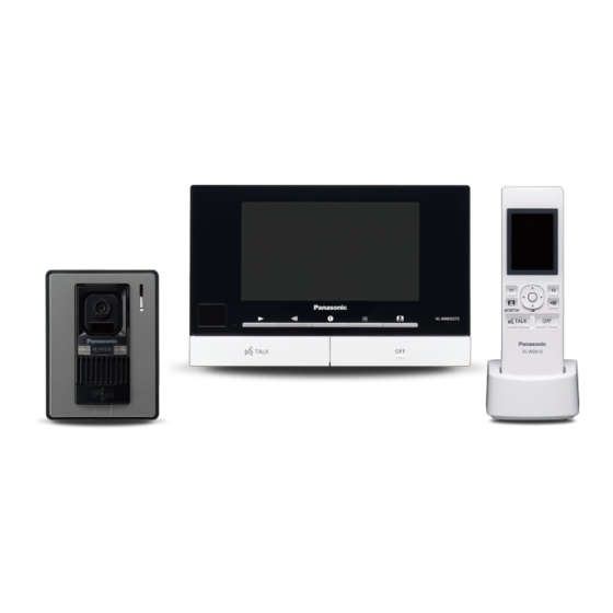
VL-SWD272BX/SWD272CX/SWD272CX1/SWD272AZ/VL-WD613CX/VL-WD613CX1 5 Location of Controls and Components Refer to the Operating Instructions. Note: You can download and refer to the Operating Instructions (Instruction book) on TSN Server. 6 Installation Instructions Refer to the Operating Instructions. Note: You can download and refer to the Operating Instructions (Instruction book) on TSN Server. -
Page 20: Service Mode
VL-SWD272BX/SWD272CX/SWD272CX1/SWD272AZ/VL-WD613CX/VL-WD613CX1 8 Service Mode 8.1. Things to do after replacing IC If repairing FLASH Memory, EEPROM, it is necessary to initialize and adjustment. The set doesn't operate if it is not executed. 8.1.1. Main Monitor Station... -
Page 21: Wireless Monitor Station
VL-SWD272BX/SWD272CX/SWD272CX1/SWD272AZ/VL-WD613CX/VL-WD613CX1 8.1.2. Wireless Monitor Station... -
Page 22: Troubleshooting Guide
VL-SWD272BX/SWD272CX/SWD272CX1/SWD272AZ/VL-WD613CX/VL-WD613CX1 9 Troubleshooting Guide 9.1. Operation Check of the Door Station Reference: • Refer to Calling Operation in Signal Route (P.49). • Refer to Talk Signal in Signal Route (P.49). - Page 23 VL-SWD272BX/SWD272CX/SWD272CX1/SWD272AZ/VL-WD613CX/VL-WD613CX1 Reference: • Refer to Image Signal in Signal Route (P.49).
- Page 24 VL-SWD272BX/SWD272CX/SWD272CX1/SWD272AZ/VL-WD613CX/VL-WD613CX1 Reference: ? Refer to AM Signal in Signal Route (P.49).
-
Page 25: Operation Check Of The Main Monitor Station
VL-SWD272BX/SWD272CX/SWD272CX1/SWD272AZ/VL-WD613CX/VL-WD613CX1 9.2. Operation Check of the Main Monitor Station... - Page 26 VL-SWD272BX/SWD272CX/SWD272CX1/SWD272AZ/VL-WD613CX/VL-WD613CX1 Reference: (*1) Defect of the Main Monitor Station Power Supply (P.29). (*5) Defect of the Main Monitor Station Video Record- (*2) Defect of the Main Monitor Station RF Communication ing(P.37). (P.33). (*6) Defect of the Communication Between the Main Moni- (*3) Defect of the Main Monitor Station Transmission(P.35).
-
Page 27: Defect Of Communication Between The Main Monitor Station And Extension Monitor
VL-SWD272BX/SWD272CX/SWD272CX1/SWD272AZ/VL-WD613CX/VL-WD613CX1 9.2.1. Defect of Communication Between the Main Monitor Station and Extension Monitor Reference: • Refer to Image Signal in Signal Route (P.49). • Refer to Talk Signal in Signal Route (P.49). • (*1) How to Remove the Main Board, Speaker and LCD [No.3] (P.56). -
Page 28: Defect Of The Extension Monitor Video Recording
VL-SWD272BX/SWD272CX/SWD272CX1/SWD272AZ/VL-WD613CX/VL-WD613CX1 9.2.2. Defect of the Extension Monitor Video Recording Reference: • Refer to Recording image Operation in Signal Route (P.49). -
Page 29: Defect Of The Main Monitor Station Power Supply
VL-SWD272BX/SWD272CX/SWD272CX1/SWD272AZ/VL-WD613CX/VL-WD613CX1 9.2.3. Defect of the Main Monitor Station Power Supply... - Page 30 VL-SWD272BX/SWD272CX/SWD272CX1/SWD272AZ/VL-WD613CX/VL-WD613CX1...
- Page 31 VL-SWD272BX/SWD272CX/SWD272CX1/SWD272AZ/VL-WD613CX/VL-WD613CX1...
- Page 32 VL-SWD272BX/SWD272CX/SWD272CX1/SWD272AZ/VL-WD613CX/VL-WD613CX1 Reference: • Refer to LCD start up in Signal Route (P.49).
-
Page 33: Defect Of The Main Monitor Station Rf Communication
VL-SWD272BX/SWD272CX/SWD272CX1/SWD272AZ/VL-WD613CX/VL-WD613CX1 9.2.4. Defect of the Main Monitor Station RF Communication Reference: • (*1) Location/avoiding noise (Main monitor station/wireless monitor station) (P.48). - Page 34 VL-SWD272BX/SWD272CX/SWD272CX1/SWD272AZ/VL-WD613CX/VL-WD613CX1 9.2.4.1. Check Point (Main monitor station) Items Check Point Procedure 1 1.8 V Supply Adjustment CL437(BB1.8V) 1.Confirm that the voltage between test point CL437 and CL109(GND) is 1.8 V ± 0.02 V. 2.Execute the command “VDD”, then check the current value.
-
Page 35: Defect Of The Main Monitor Station Transmission
VL-SWD272BX/SWD272CX/SWD272CX1/SWD272AZ/VL-WD613CX/VL-WD613CX1 9.2.5. Defect of the Main Monitor Station Transmission Reference: (*1) Defect of the Wireless Monitor Station Reception (P.46). -
Page 36: Defect Of The Main Monitor Station Reception
VL-SWD272BX/SWD272CX/SWD272CX1/SWD272AZ/VL-WD613CX/VL-WD613CX1 9.2.6. Defect of the Main Monitor Station Reception Reference: (*1) Defect of the Wireless Monitor Station Transmission(P.45). -
Page 37: Defect Of The Main Monitor Station Video Recording
VL-SWD272BX/SWD272CX/SWD272CX1/SWD272AZ/VL-WD613CX/VL-WD613CX1 9.2.7. Defect of the Main Monitor Station Video Recording Reference: • Refer to Recording Image Operation in Signal Route (P.49). -
Page 38: Defect Of The Communication Between The Main Monitor Station And The Door Station
VL-SWD272BX/SWD272CX/SWD272CX1/SWD272AZ/VL-WD613CX/VL-WD613CX1 9.2.8. Defect of the Communication Between the Main Monitor Station and the Door Sta- tion Reference: • Refer to Talk Signal in Signal Route (P.49). • Refer to Image Signal in Signal Route (P.49). • (*1) How to Remove the Main Board, Speaker and LCD [No.3] (P.56). -
Page 39: Defect Of The Communication Between The Extention Monitor Station And The Door Station
VL-SWD272BX/SWD272CX/SWD272CX1/SWD272AZ/VL-WD613CX/VL-WD613CX1 9.2.9. Defect of the Communication Between the Extention Monitor Station and the Door Station Reference: • Refer to Talk Signal in Signal Route (P.49). • Refer to Image Signal in Signal Route (P.49). • (*1) How to Remove the Main Board, Speaker and LCD [No.3] (P.56). -
Page 40: Operation Check Of The Wireless Monitor Station
VL-SWD272BX/SWD272CX/SWD272CX1/SWD272AZ/VL-WD613CX/VL-WD613CX1 9.3. Operation Check of the Wireless Monitor Station Reference: (*1) Defect of the Wireless Monitor Station Power Sup- (*4) Defect of the Wireless Monitor Station Transmis- ply(P.41). sion(P.45). (*2) Defect of the Wireless Monitor Station LCD(P.42). (*5) Defect of the Wireless Monitor Station Reception(P.46). -
Page 41: Defect Of The Wireless Monitor Station Power Supply
VL-SWD272BX/SWD272CX/SWD272CX1/SWD272AZ/VL-WD613CX/VL-WD613CX1 9.3.1. Defect of the Wireless Monitor Station Power Supply... -
Page 42: Defect Of The Wireless Monitor Station
VL-SWD272BX/SWD272CX/SWD272CX1/SWD272AZ/VL-WD613CX/VL-WD613CX1 9.3.2. Defect of the Wireless Monitor Station LCD Reference: (*1) How to Remove the Main Board and LCD [No.2] (P.66). -
Page 43: Defect Of The Wireless Monitor Station Radio Communication
VL-SWD272BX/SWD272CX/SWD272CX1/SWD272AZ/VL-WD613CX/VL-WD613CX1 9.3.3. Defect of the Wireless Monitor Station Radio Communication Reference: (*1) Location/avoiding noise (Main monitor station/wireless monitor station) (P.48). - Page 44 VL-SWD272BX/SWD272CX/SWD272CX1/SWD272AZ/VL-WD613CX/VL-WD613CX1 9.3.3.1. Check Point (Wireless monitor station) Items Check Point Procedure 1.8 V Supply Adjustment CL3 (BB1.8V) 1.Confirm that the voltage between test point CL3 and CL9(GND) is 1.8 V ± 0.02 V. 2.Execute the command “VDD”, then check the current value.
-
Page 45: Defect Of The Wireless Monitor Station Transmission
VL-SWD272BX/SWD272CX/SWD272CX1/SWD272AZ/VL-WD613CX/VL-WD613CX1 9.3.4. Defect of the Wireless Monitor Station Transmission Reference: (*1) Defect of the Main Monitor Station Reception (P.36). -
Page 46: Defect Of The Wireless Monitor Station Reception
VL-SWD272BX/SWD272CX/SWD272CX1/SWD272AZ/VL-WD613CX/VL-WD613CX1 9.3.5. Defect of the Wireless Monitor Station Reception Reference: (*1) Defect of the Main Monitor Station Transmission (P.35). -
Page 47: Defect Of The Wireless Monitor Station Charging
VL-SWD272BX/SWD272CX/SWD272CX1/SWD272AZ/VL-WD613CX/VL-WD613CX1 9.3.6. Defect of the Wireless Monitor Station Charging... -
Page 48: Before Using
Location/avoiding noise (Main monitor station/wireless monitor station) The main monitor, wireless monitor, and other compatible Panasonic units use radio waves to communicate with each other. (The product operates in the frequency range of 1.88 GHz to 1.90 GHz, and the RF transmission power is 250 mW (max.).) •... -
Page 49: Signal Route
VL-SWD272BX/SWD272CX/SWD272CX1/SWD272AZ/VL-WD613CX/VL-WD613CX1 9.5. Signal Route This chapter provides the testing procedures required for the P.C.B. parts. A signal route to be tested is determined depending upon purposes. The signal mainly flowing on this route is analog. You can trace the signal with an oscilloscope. The signal flow on each route is shown in the Check Sheet here. - Page 50 VL-SWD272BX/SWD272CX/SWD272CX1/SWD272AZ/VL-WD613CX/VL-WD613CX1...
- Page 51 VL-SWD272BX/SWD272CX/SWD272CX1/SWD272AZ/VL-WD613CX/VL-WD613CX1...
- Page 52 VL-SWD272BX/SWD272CX/SWD272CX1/SWD272AZ/VL-WD613CX/VL-WD613CX1...
- Page 53 VL-SWD272BX/SWD272CX/SWD272CX1/SWD272AZ/VL-WD613CX/VL-WD613CX1...
- Page 54 VL-SWD272BX/SWD272CX/SWD272CX1/SWD272AZ/VL-WD613CX/VL-WD613CX1...
-
Page 55: Disassembly And Assembly Instructions
VL-SWD272BX/SWD272CX/SWD272CX1/SWD272AZ/VL-WD613CX/VL-WD613CX1 10 Disassembly and Assembly Instructions 10.1. Main Monitor Station 10.1.1. How to Remove the AC Cord [No.1] n Procedure No.1 1. Remove a screw 2. Remove the Power cord cover. 3. Loosen screws and pull out the wires of the Power cord as shown in Fig. -
Page 56: How To Remove The Main Board, Speaker And Lcd [No.3]
VL-SWD272BX/SWD272CX/SWD272CX1/SWD272AZ/VL-WD613CX/VL-WD613CX1 10.1.3. How to Remove the Main Board, Speaker and LCD [No.3] n Procedure No.1No.2No.3 1. Remove 2 screws 2. Unhook the tab of the Push Button (Fig.1). 3. Remove the Main Board from Cabinet body. 4. Unhook the 4 tabs of the LCD holder. -
Page 57: Door Station
VL-SWD272BX/SWD272CX/SWD272CX1/SWD272AZ/VL-WD613CX/VL-WD613CX1 10.2. Door Station 10.2.1. How to Remove the Mounting Base [No.1] n Procedure No.1 1. Open the screw cover, as shown in Fig. F. 2. Loose 1 screw (D). 3. Remove the Mounting base, as shown in Fig. G. -
Page 58: How To Remove The Main Board And Camera Unit [No.2]
VL-SWD272BX/SWD272CX/SWD272CX1/SWD272AZ/VL-WD613CX/VL-WD613CX1 10.2.2. How to Remove the Main Board and Camera Unit [No.2] n Procedure No.1→No.2 1. Remove 2 screws (E). 2. Please remove the cabinet cover from cabinet body with care to the tabs. 3. Remove the solder on the lead wire-A and lead wire-B. -
Page 59: How To Remove The Mic Board And Speaker [No.3]
VL-SWD272BX/SWD272CX/SWD272CX1/SWD272AZ/VL-WD613CX/VL-WD613CX1 10.2.3. How to Remove the Mic Board and Speaker [No.3] n Procedure No.1→No.2→No.3 1. Remove the Mic board. 2. Remove 2 screws (F). 3. Remove the Speaker. - Page 60 VL-SWD272BX/SWD272CX/SWD272CX1/SWD272AZ/VL-WD613CX/VL-WD613CX1 10.2.3.1. Note for Microphone Assembly (for anti-feedback)
-
Page 61: How To Remove The Front Panel [No.4]
VL-SWD272BX/SWD272CX/SWD272CX1/SWD272AZ/VL-WD613CX/VL-WD613CX1 10.2.4. How to Remove the Front Panel [No.4] n Procedure No.4 1. After unhook the 6 tabs as shown in Fig. J, remove the Front panel. -
Page 62: Installation Of The Lead Wires
VL-SWD272BX/SWD272CX/SWD272CX1/SWD272AZ/VL-WD613CX/VL-WD613CX1 10.2.5. Installation of the lead wires When assembling the door station, route the lead wires as shown in the figure below, and be careful that they do not get caught. 10.2.6. Item to be checked after completion of assembly (camera lens angle adjustment) After completing assembly work, move the angle adjustment lever on the rear surface in the left and right directions, and confirm that it moves all the way. -
Page 63: Wireless Monitor Station
VL-SWD272BX/SWD272CX/SWD272CX1/SWD272AZ/VL-WD613CX/VL-WD613CX1 10.3. Wireless Monitor Station 10.3.1. How to Remove the Cabinet Cover [No.1] n Procedure No.1 1. Remove the battery lid by sliding the cover to the direction as shown. 2. Remove the batteries and 2 screws (P). 3. Hold the cabinet and open it slightly (about 5mm). - Page 64 VL-SWD272BX/SWD272CX/SWD272CX1/SWD272AZ/VL-WD613CX/VL-WD613CX1 4. Insert a JIG (PQDJ10006Y) between the cabinet body and the cabinet cover, then pull it along the gap to open the cabinet. 5. Open the opposite side at the same way as well.
- Page 65 VL-SWD272BX/SWD272CX/SWD272CX1/SWD272AZ/VL-WD613CX/VL-WD613CX1 6. Open the cabinet cover gently with careful handling of the speaker lead connections. 7. Remove the solder on the speaker lead wire, then remove the cabinet cover.
-
Page 66: How To Remove The Main Board And Lcd [No.2]
VL-SWD272BX/SWD272CX/SWD272CX1/SWD272AZ/VL-WD613CX/VL-WD613CX1 10.3.2. How to Remove the Main Board and LCD [No.2] n Procedure No.1→No.2 1. Remove 2 screws (Q), then remove the Main board from Cabinet body. 2. Remove the solder on the battery terminals. 3. Remove the battery holder by unhooking 2 tabs. - Page 67 VL-SWD272BX/SWD272CX/SWD272CX1/SWD272AZ/VL-WD613CX/VL-WD613CX1 4. Remove the LCD flat cable from the Main board, as shown in Fig. K. 5. Remove the LCD holder from Main board by unhooking 2 tabs. 6. Remove the LCD from LCD holder by unhooking 2 tabs.
- Page 68 VL-SWD272BX/SWD272CX/SWD272CX1/SWD272AZ/VL-WD613CX/VL-WD613CX1 10.3.2.1. Notice for Installing the coil 1. Solder the coil which is packed with Main Board. Solder one end of lead wire of coil from its outside to the upper side(+ side) position of Microphone on the Main Board.
-
Page 69: How To Remove The Speaker [No.3]
VL-SWD272BX/SWD272CX/SWD272CX1/SWD272AZ/VL-WD613CX/VL-WD613CX1 10.3.3. How to Remove the Speaker [No.3] n Procedure No.1→No.3 1. Remove the speaker holder by a turning. 2. Remove the Speaker from cabinet cover. -
Page 70: How To Remove The Battery Board [No.4]
VL-SWD272BX/SWD272CX/SWD272CX1/SWD272AZ/VL-WD613CX/VL-WD613CX1 10.3.4. How to Remove the Battery Board [No.4] n Procedure No.1→No.4 1. Remove the solder on the Battery Board. 2. Remove the Battery Board from cabinet cover. 10.3.5. Charger Unit 1. Remove the screw (M). 2. Remove the cabinet cover and Charger Board from the cabinet body. -
Page 71: Measurements And Adjustments
VL-SWD272BX/SWD272CX/SWD272CX1/SWD272AZ/VL-WD613CX/VL-WD613CX1 11 Measurements and Adjustments 11.1. Main Monitor Station 11.1.1. Main Board 11.1.1.1. Connections When replacing the main board (Monitor Station), please refer to the following items for adjusting. - Page 72 VL-SWD272BX/SWD272CX/SWD272CX1/SWD272AZ/VL-WD613CX/VL-WD613CX1 11.1.1.2. When replacing BBIC and X'tal n Preparation: 1. PC setting refer to “Main Monitor Station (P.20). 2. Supply AC 230V. Note: Test points: Refer to Main Board (Bottom View) (P.99). Items Check Point Procedure 1 1.8 V Supply Adjustment CL437(BB1.8V) 1.Confirm that the voltage between test point CL437 and CL109 (GND) is...
-
Page 73: Factory Mode
VL-SWD272BX/SWD272CX/SWD272CX1/SWD272AZ/VL-WD613CX/VL-WD613CX1 11.1.2. Factory Mode n Entering Factory Mode: 1. Turn AC Power “ON”, while pressing [OFF] button, [TALK] button and [F4] at the same time, about 5 seconds or more. (FACTORY MODE screen is displayed.) n In order to exit Factory Mode:... - Page 74 VL-SWD272BX/SWD272CX/SWD272CX1/SWD272AZ/VL-WD613CX/VL-WD613CX1 11.1.2.1. Factory Setup Initialize the logs and the all parameters except for the factory adjusted value, and delete the recorded images. 1. Select “FACTORY SETUP” by [F2] or [F3]. 2. Press [F4 (DECIDE)]. 3. Press [F4 (RUN)]. 4. Press [F1 (RESET)].
- Page 75 VL-SWD272BX/SWD272CX/SWD272CX1/SWD272AZ/VL-WD613CX/VL-WD613CX1 11.1.2.2. White Balance Adjustment The adjustment is done only when the color of the LCD display has changed after you have replaced the LCD. (Basically, adjustment is unnecessary.) 1. Select “TECHNICAL MODE 1” by [F2] or [F3]. 2. Select “WHITE BALANCE” by [F2] or [F3].
-
Page 76: Door Station
VL-SWD272BX/SWD272CX/SWD272CX1/SWD272AZ/VL-WD613CX/VL-WD613CX1 4. Adjust the white balance by R Gain and B Gain. Select the color to be adjust as below [F1] (>>): (Select Digit) [F2] ( ), F3 ( ): (Change Value) Press [F4 (DECIDE)] Adjust the white balance as below [F1] (>>): (Select Digit) -
Page 77: Wireless Monitor Station
VL-SWD272BX/SWD272CX/SWD272CX1/SWD272AZ/VL-WD613CX/VL-WD613CX1 11.3. Wireless Monitor Station 11.3.1. Connections When replacing the main board (Wireless Monitor Station), Please refer to the following items for adjusting. -
Page 78: When Replacing Bbic And X'tal
VL-SWD272BX/SWD272CX/SWD272CX1/SWD272AZ/VL-WD613CX/VL-WD613CX1 11.3.2. When replacing BBIC and X’tal n Preparation: 1. PC setting refer to “Wireless Monitor Station (P.21). 2. Supply DC 2.6V at CL5. Note: Test points: Refer to Main Board (Bottom View) (P.103). Items Check Point Procedure 1 1.8 V Supply Adjustment CL3(BB1.8V) -
Page 79: After Replacing Main Board (For Wireless Monitor Station)
VL-SWD272BX/SWD272CX/SWD272CX1/SWD272AZ/VL-WD613CX/VL-WD613CX1 11.3.3. After replacing Main board (for Wireless monitor station) n Entering Maintenance Mode: 1. Press simultaneously. [OFF] [Monitor] 2. Press twice for entering "MAINTENANCE MODE". [TALK] Items Operations Points to be checked (1) Volume check 1. Press [MONITOR] key twice. - Page 80 VL-SWD272BX/SWD272CX/SWD272CX1/SWD272AZ/VL-WD613CX/VL-WD613CX1 Items Operations Points to be checked (5) KEY check 1. Press [MONITOR] key, then press [F1] key. LCD: KEY CODE [KEY CODE] 2. Press all keys one by one except [OFF] key. Pressed key name appears. 3. Press [OFF] key at last.
-
Page 81: Miscellaneous
VL-SWD272BX/SWD272CX/SWD272CX1/SWD272AZ/VL-WD613CX/VL-WD613CX1 12 Miscellaneous 12.1. How to Replace the Flat Package IC Even if you do not have the special tools (for example, a spot heater) to remove the Flat IC, with some solder (large amount), a soldering iron and a cutter knife, you can easily remove the ICs that have more than 100 pins. -
Page 82: Schematic Diagram
VL-SWD272BX/SWD272CX/SWD272CX1/SWD272AZ/VL-WD613CX/VL-WD613CX1 13 Schematic Diagram 13.1. Main Monitor Station 13.1.1. Main Board (1) / External I/F C611 1u 6.3 R611 330 RL640 C621 1u 6.3 D640 R621 330 C630 R630 D621 D611 L643 L642 L641 R633 C659 L640 L644 1000p RL641... -
Page 83: Main Board (2) / Bbic
VL-SWD272BX/SWD272CX/SWD272CX1/SWD272AZ/VL-WD613CX/VL-WD613CX1 13.1.2. Main Board (2) / BBIC CL573 CL572 CL574 CL571 D560 R584 CF571 D561 R588 C563 C562 100k 100k CF572 R565 R564 C565 C564 3300p R400 3300p 4.7k R572 R573 R583 R574 R571 R589 100k C585 C575 6.3V 22uF... -
Page 84: Main Board (3) / Dpjp3_Key
VL-SWD272BX/SWD272CX/SWD272CX1/SWD272AZ/VL-WD613CX/VL-WD613CX1 13.1.3. Main Board (3) / DPJP3_KEY C100 2200p D100 4.71V C102 4.7k 0.1u 16 R102 IC101 R107 1 GND 220p 2 VDD C111 C106 1000p 0.01u 25 C105 C103 R110 16V 1uF 16V 1uF C107 C104 C112 6.3V C340 0.01u... -
Page 85: Main Board (4) / Lcd
VL-SWD272BX/SWD272CX/SWD272CX1/SWD272AZ/VL-WD613CX/VL-WD613CX1 13.1.4. Main Board (4) / LCD C230 1uF 6.3V R231 R230 C231 Q230 Gth=1.8V 25V 10uF C232 16V 0.1uF C233 D230 C234 16V 0.1uF R235 2.2k C237 16V 0.1uF C238 1 COMP 3300pF 5.1k 2 FB FCLK 3 ENB... -
Page 86: Main Board (5) / External I/F_Electric Lock
VL-SWD272BX/SWD272CX/SWD272CX1/SWD272AZ/VL-WD613CX/VL-WD613CX1 13.1.5. Main Board (5) / External I/F_Electric lock CL605 CL606 CL607 CL608 CL604 CL603 CL609 CL621 CL610 CL602 CL622 CL611 CL601 CL623 CL612 CL624 CL613 CL614 CL615 CL616 CL617 CL618 C893 C892 R881 R880 150 C881 150 C880 0.1u 0.1u... -
Page 87: Main Board (6) / Led_Key
VL-SWD272BX/SWD272CX/SWD272CX1/SWD272AZ/VL-WD613CX/VL-WD613CX1 13.1.6. Main Board (6) / LED_KEY D281 R281 CL176 CL170 CL171 CL172 CL173 CL174 CL175 SW176 SW170 SW171 SW172 SW173 SW174 SW175 VL-SWD272/VL-MWD272: Main Board No.6: LED_KEY... -
Page 88: Main Board (7) / Dcdc
VL-SWD272BX/SWD272CX/SWD272CX1/SWD272AZ/VL-WD613CX/VL-WD613CX1 13.1.7. Main Board (7) / DCDC C901 C900 10uF C903 0.1u C904 0.1u C905 10uF C907 C902 0.01u 25 C906 10uF C921 NC C911 C920 C930 C910 25V 10uF 25V 10uF 25V 10uF R921 R931 R922 R912 R911 R932 60.4k... -
Page 89: Main Board (8) / Pbx_I/F
VL-SWD272BX/SWD272CX/SWD272CX1/SWD272AZ/VL-WD613CX/VL-WD613CX1 13.1.8. Main Board (8) / PBX_I/F R809 0.25 C802 10u 10V R803 D803 C801 R801 0.01u R812 R808 4.7k C812 C811 0.22u 16 C820 IC801 AOUT R813 27k A-IN BOUT C816 100p A+IN B-IN B+IN C819 C822 3p C821... -
Page 90: Main Board (9) / Am Communication_Base
VL-SWD272BX/SWD272CX/SWD272CX1/SWD272AZ/VL-WD613CX/VL-WD613CX1 13.1.9. Main Board (9) / AM communication_base unit L720 L719 L718 L717 L713 L711 L721 C721 L728 C724 L722 C722 L729 C725 L723 C723 L730 C729 C710 0.1u 16 C707 C715 C748 1000p 1000p 1000p R709 R779 R724 R713... -
Page 91: Main Board (10) / Am Communication_Expansion
VL-SWD272BX/SWD272CX/SWD272CX1/SWD272AZ/VL-WD613CX/VL-WD613CX1 13.1.10. Main Board (10) / AM communication_expansion RL759 D759 C759 NC C765 100p C766 100p R762 NC R768 R763 IC760 1 AOUT R770 2 A-IN 8.2k BOUT 3 A+IN B-IN C777 C776 4 V- 100p B+IN C772 NC C778... -
Page 92: Main Board (11) / Power
VL-SWD272BX/SWD272CX/SWD272CX1/SWD272AZ/VL-WD613CX/VL-WD613CX1 13.1.11. Main Board (11) / POWER 750V C1 0.1uF 310V 27uF 450V 15uF 450V 2000V 1000p 1uF 25V 1000pF 50V R8 0.1 1k 0.22uF 25V C26 33pF C5 2200pF 1000V 2000V R10 0.125 220 R11 0.125 2.2k C14 470u 25... -
Page 93: Main Board (12) / Mic
VL-SWD272BX/SWD272CX/SWD272CX1/SWD272AZ/VL-WD613CX/VL-WD613CX1 13.1.12. Main Board (12) / MIC MIC+ 2:1B MIC- 2:1B MIC800 1SH102 1SH101 NC: No Components VL-SWD272/VL-MWD272: Main Board No.12: MIC... -
Page 94: Door Station
VL-SWD272BX/SWD272CX/SWD272CX1/SWD272AZ/VL-WD613CX/VL-WD613CX1 13.2. Door Station 13.2.1. Main Board/MIC Board... -
Page 95: Wireless Monitor Station
VL-SWD272BX/SWD272CX/SWD272CX1/SWD272AZ/VL-WD613CX/VL-WD613CX1 13.3. Wireless Monitor Station 13.3.1. Main Board C500 ROW[0] *D210 C200 *D211 C201 10p ROW[1] C400 *D100 R503 0.068u C202 10p C401 R500 0.1u 16 *C272 *R100 C408 *D101 D200 LED[1] *C258 NC16 C501 ROW[2] *C271 D201 *C261 NC... -
Page 96: Poly Switch Board
VL-SWD272BX/SWD272CX/SWD272CX1/SWD272AZ/VL-WD613CX/VL-WD613CX1 13.3.2. Poly Switch Board Battery Battery VL-SWD272/VL-WD613: Poly Switch Board... -
Page 97: Charger
VL-SWD272BX/SWD272CX/SWD272CX1/SWD272AZ/VL-WD613CX/VL-WD613CX1 13.4. Charger 13.4.1. Charger Board 1/2W OUTPUT INPUT VOUT ADJ/GND 1/4W Black 200mA Black Charge+ 200mA Charge- VL-SW251/VL-W605: Charger Board... -
Page 98: Printed Circuit Board
VL-SWD272BX/SWD272CX/SWD272CX1/SWD272AZ/VL-WD613CX/VL-WD613CX1 14 Printed Circuit Board 14.1. Main Monitor Station 14.1.1. Main Board (Component View) VL-MWD272: Main Board (COMPONENT VIEW) -
Page 99: Main Board (Bottom View)
VL-SWD272BX/SWD272CX/SWD272CX1/SWD272AZ/VL-WD613CX/VL-WD613CX1 14.1.2. Main Board (Bottom View) C130 C129 C115 R350 C116 R354 C120 C117 C114 C121 C143 C149 C113 C201 C202 C205 C207 C209 C211 C213 C216 C218 C219 C144 C220 C221 C222 C223 C224 C225 C226 C136 C227 C217... -
Page 100: Door Station Board
VL-SWD272BX/SWD272CX/SWD272CX1/SWD272AZ/VL-WD613CX/VL-WD613CX1 14.2. Door Station Board 14.2.1. Main Board (Component View) LED200 LED201 R133 C115 D101 IC204 R128 C119 C130 C103 L103 C128 R122 R219 C122 IC100 C123 C220 C116 R120 C120 R212 R119 Q203 Q207 Q205 IC102 Q206 R215 C131... -
Page 101: Mic Board
VL-SWD272BX/SWD272CX/SWD272CX1/SWD272AZ/VL-WD613CX/VL-WD613CX1 14.2.2. MIC Board (Component View) (Bottom View) MIC1 VL-V522L MIC Board... -
Page 102: Wireless Monitor Station Board
VL-SWD272BX/SWD272CX/SWD272CX1/SWD272AZ/VL-WD613CX/VL-WD613CX1 14.3. Wireless Monitor Station Board 14.3.1. Main Board (Component View) C260 C272 C265 R256 C267 C269 R204 R301 C204 R202 C308 R205 C205 L401 C206 L400 R608 C104 C105 C106 C600 R551 C553 C118 C103 C102 C101 C100 C251... -
Page 103: Main Board (Bottom View)
VL-SWD272BX/SWD272CX/SWD272CX1/SWD272AZ/VL-WD613CX/VL-WD613CX1 14.3.2. Main Board (Bottom View) C264 C502 R501 JOINT301 C218 R502 Q500 R500 C500 C611 CL16 R609 R607 C609 C608 C256 C607 C255 C624 C635 C625 C626 C634 C627 C620 C631 C621 C630 C622 C623 SW11 SW10 SW16 SW18... -
Page 104: Appendix Information Of Schematic Diagram
VL-SWD272BX/SWD272CX/SWD272CX1/SWD272AZ/VL-WD613CX/VL-WD613CX1 15 Appendix Information of Schematic Diagram Note: 1. DC voltage measurements are taken with an oscilloscope or a tester with a ground. 2. The schematic diagrams and circuit board may be modified at any time with the development of new technology. -
Page 105: Exploded View And Replacement Parts List
VL-SWD272BX/SWD272CX/SWD272CX1/SWD272AZ/VL-WD613CX/VL-WD613CX1 16 Exploded View and Replacement Parts List 16.1. Exploded View 16.1.1. Main Monitor Station PCB1... -
Page 106: Door Station
VL-SWD272BX/SWD272CX/SWD272CX1/SWD272AZ/VL-WD613CX/VL-WD613CX1 16.1.2. Door Station PCB100 PCB101 E101... -
Page 107: Wireless Monitor Station
VL-SWD272BX/SWD272CX/SWD272CX1/SWD272AZ/VL-WD613CX/VL-WD613CX1 16.1.3. Wireless Monitor Station 210-4 210-3 210-2 210-1 E201 Bottom side PCB201 E205 E203 E204 E202 (*1) The rechargeable Ni-MH battery is available through sales route (*1) of Panasonic. -
Page 108: Charger
VL-SWD272BX/SWD272CX/SWD272CX1/SWD272AZ/VL-WD613CX/VL-WD613CX1 16.1.4. Charger PCB301... -
Page 109: Accessories And Packing Materials Location
VL-SWD272BX/SWD272CX/SWD272CX1/SWD272AZ/VL-WD613CX/VL-WD613CX1 16.1.5. Accessories and Packing Materials Location 16.1.5.1. VL-SWD272BX/VL-SWD272CX/VL-SWD272CX1/VL-SWD272AZ (*2) A1〜A4 (*1) Note: (*1) This pad is piece of Ref No. P4. (*2) "A3" is VL-SWD272BX/VL-SWD272AZ only. "A4" is VL-SWD272AZ only. - Page 110 VL-SWD272BX/SWD272CX/SWD272CX1/SWD272AZ/VL-WD613CX/VL-WD613CX1 16.1.5.2. VL-SVD272BX/VL-SVD272CX/VL-SVD272AZ (*2) 〜A104 A101 P104 P105 A105 P101 P106 P108 P107 A106 A107 P109 P102 (*1) P103 Note: (*1) This pad is piece of Ref No. P102. (*2) "A103" is VL-SVD272BX/VL-SVD272AZ only. "A104" is VL-SVD272AZ only.
- Page 111 VL-SWD272BX/SWD272CX/SWD272CX1/SWD272AZ/VL-WD613CX/VL-WD613CX1 16.1.5.3. VL-MWD272BX/VL-MWD272CX/VL-MWD272CX1/VL-MWD272AZ (Optional Unit) (*2) A201〜A204 P201 P202 P203 A206 A205 P204 P205 (*1) P206 Note: (*1) This pad is piece of Ref No. P205. (*2) "A203" is VL-SVD272BX/VL-SVD272AZ only. "A204" is VL-SVD272AZ only.
- Page 112 VL-SWD272BX/SWD272CX/SWD272CX1/SWD272AZ/VL-WD613CX/VL-WD613CX1 16.1.5.4. VL-WD613CX/VL-WD613CX1 (Optional Unit) A301 P303 P304 A302 P302 P301 P305...
-
Page 113: Replacement Parts List
VL-SWD272BX/SWD272CX/SWD272CX1/SWD272AZ/VL-WD613CX/VL-WD613CX1 16.2. Replacement Parts List Note: Safety Ref. Part No. Part Name & Descrip- Remarks 1. RTL (Retention Time Limited) tion The marking (RTL) indicates that the Retention Time is PNMH1448Z LCD SHIELD L5EDDYY00882 LCD limited for this item. PNZEAD272CX... - Page 114 VL-SWD272BX/SWD272CX/SWD272CX1/SWD272AZ/VL-WD613CX/VL-WD613CX1 Safety Ref. Part No. Part Name & Descrip- Remarks Safety Ref. Part No. Part Name & Descrip- Remarks tion tion (TRANSISTORS) D760 DZ2J056M0L DIODE(SI) B1ABMF000022 TRANSISTOR(SI) D801 DA3J101F0L DIODE(SI) Q160 DRC9114E0L TRANSISTOR(SI) D802 DA3J101F0L DIODE(SI) Q161 DRC9114E0L TRANSISTOR(SI) D804...
- Page 115 VL-SWD272BX/SWD272CX/SWD272CX1/SWD272AZ/VL-WD613CX/VL-WD613CX1 Safety Ref. Part No. Part Name & Descrip- Remarks Safety Ref. Part No. Part Name & Descrip- Remarks tion tion L716 J0JCC0000092 IC FILTER ERJ8GEY0R00 L717 J0JCC0000092 IC FILTER ERJ3GEYJ102 L718 G1C470MA0072 COIL PQ4R10XJ222 2.2k L719 G1C470MA0072 COIL PQ4R10XJ221...
- Page 116 VL-SWD272BX/SWD272CX/SWD272CX1/SWD272AZ/VL-WD613CX/VL-WD613CX1 Safety Ref. Part No. Part Name & Descrip- Remarks Safety Ref. Part No. Part Name & Descrip- Remarks tion tion R408 D1H81034A042 COMPONENTS PARTS R639 ERJ2GEJ472X 4.7k R409 ERJ3BQJ1R0V R640 ERJ3GEYJ561 R410 D1H43302A014 COMPONENTS PARTS R641 PQ4R10XJ100 R412 D0GA563ZA006 56k...
- Page 117 VL-SWD272BX/SWD272CX/SWD272CX1/SWD272AZ/VL-WD613CX/VL-WD613CX1 Safety Ref. Part No. Part Name & Descrip- Remarks Safety Ref. Part No. Part Name & Descrip- Remarks tion tion R765 D0GA104JA021 100k F1H1E224A098 0.22 R766 ERJ2GEJ393X F1L1H106A125 10 R767 ERJ2GEJ822 8.2k F2A2W150A349 15 R768 ERJ2GEJ103 F1BAF222A085 0.0022 R769...
- Page 118 VL-SWD272BX/SWD272CX/SWD272CX1/SWD272AZ/VL-WD613CX/VL-WD613CX1 Safety Ref. Part No. Part Name & Descrip- Remarks Safety Ref. Part No. Part Name & Descrip- Remarks tion tion C207 ECUE1H330JCQ 33p C425 ECUE1C104KBQ 0.1 C208 ECUE1H330JCQ 33p C426 ECUE1C104KBQ 0.1 C209 ECUE1H330JCQ 33p C427 ECUE1C104KBQ 0.1 C210...
- Page 119 VL-SWD272BX/SWD272CX/SWD272CX1/SWD272AZ/VL-WD613CX/VL-WD613CX1 Safety Ref. Part No. Part Name & Descrip- Remarks Safety Ref. Part No. Part Name & Descrip- Remarks tion tion C620 ECUE1H330JCQ 33p C766 ECUE1H101JCQ 100p C621 ECUE0J105KBQ 1 C767 ECUE1C104KBQ 0.1 C630 ECUE1H100DCQ 10p C768 ECUE1H391KBQ 390p C631 ECUE1H152KBQ 0.0015...
-
Page 120: Door Station
VL-SWD272BX/SWD272CX/SWD272CX1/SWD272AZ/VL-WD613CX/VL-WD613CX1 16.2.2.2. Main P.C. Board Parts Safety Ref. Part No. Part Name & Descrip- Remarks tion (*4) When replacing Main board of door station, confirm opera- (OTHERS) tion. (Refer to Door Station (P.76)). AL600 D4EDY201A035 VARISTOR CF571 D4ZZ00000039 VARISTOR CF572... - Page 121 VL-SWD272BX/SWD272CX/SWD272CX1/SWD272AZ/VL-WD613CX/VL-WD613CX1 Safety Ref. Part No. Part Name & Description Remarks Safety Ref. Part No. Part Name & Description Remarks R227 ERJ2GEJ101 (TRANSFORMERS) R228 ERJ2GEJ101 G5ZZ00000110 TRANSFORMER R232 ERJ2GEJ750 R233 ERJ2GEJ112X 1.1k (CRYSTAL OSCILLATORS) R234 ERJ2GEJ222 2.2k H2D200500011 CERAMIC FILTER R302...
-
Page 122: Wireless Monitor Station
VL-SWD272BX/SWD272CX/SWD272CX1/SWD272AZ/VL-WD613CX/VL-WD613CX1 Safety Ref. Part No. Part Name & Description Remarks 16.2.3.2. Main P.C. Board Parts C208 ECUE1C104KBQ 0.1 C209 ECUE1H101JCQ 100p C210 ECUE1C104KBQ 0.1 (*5) When replacing IC1, IC4 or X1, make adjustments. C211 ECUE1C104KBQ 0.1 (Refer to When replacing BBIC and X’tal (P.78)). - Page 123 VL-SWD272BX/SWD272CX/SWD272CX1/SWD272AZ/VL-WD613CX/VL-WD613CX1 Safety Ref. Part No. Part Name & Descrip- Remarks Safety Ref. Part No. Part Name & Descrip- Remarks tion tion ERJ2GEJ102 ECUV1A105KBV 1 ERJ2GEJ101 ECUV1A105KBV 1 D1H810240004 1k F1H1A105A036 1 ERJ2GEJ272 2.7k ECUE1H101JCQ 100p ERJ2GEJ272 2.7k ECUE1H100DCQ 10p EXB24V272J 2.7k...
-
Page 124: Charger Unit
VL-SWD272BX/SWD272CX/SWD272CX1/SWD272AZ/VL-WD613CX/VL-WD613CX1 Safety Ref. Part No. Part Name & Descrip- Remarks Safety Ref. Part No. Part Name & Descrip- Remarks tion tion C601 ECUE1C104KBQ 0.1 G1C100MA0395 COIL C602 ECUE1C104KBQ 0.1 C607 ECUE1H101JCQ 100p (RESISTORS) C608 ECUE1H101JCQ 100p ERJ3EKF1202 C609 ECUE1H470JCQ 47p... -
Page 125: Accessories And Packing Materials
XZB05X08A04 PROTECTION COVER, (*8) You can download and refer to the “Operating Instructions SCREW (Instruction book)” and “Installation Guide (Leaflet)” on TSN Server. 16.2.5.3. VL-SWD272AZ 16.2.5.1. VL-SWD272BX Safety Ref. Part No. Part Name & Descrip- Remarks tion Safety Ref. - Page 126 VL-SWD272BX/SWD272CX/SWD272CX1/SWD272AZ/VL-WD613CX/VL-WD613CX1 16.2.5.5. VL-SVD272CX Safety Ref. Part No. Part Name & Descrip- Remarks tion P204 XZB05X08A04 PROTECTION COVER, SCREW Safety Ref. Part No. Part Name & Descrip- Remarks P205 PNPN1548Z CUSHION tion P206 PNPK4088001Z GIFT BOX A101 PNQX8321Z INSTRUCTION BOOK(*8) A102...
-
Page 127: Fixtures And Tools
VL-SWD272BX/SWD272CX/SWD272CX1/SWD272AZ/VL-WD613CX/VL-WD613CX1 Safety Ref. Part No. Part Name & Descrip- Remarks tion P305 PNYEAWD613CX INDICATION PLATE-LABEL (for VL-WD613CX) PNYEAD613CX1 INDICATION PLATE-LABEL (for VL-WD613CX1) 16.2.6. Fixtures and Tools (*9) This is used for installing the ID NUMBER into FLASH MEMORY. (Refer to Things to do after replacing IC (P.20)). - Page 128 VL-SWD272BX/SWD272CX/SWD272CX1/SWD272AZ/VL-WD613CX/VL-WD613CX1 17 Change Information Ver. No. Main Revision Contents Issue First version September, 2017 Add destination models (VL-SWD272CX1,VL-MWD272CX1,VL-WD613CX1). May, 2019...