Table of Contents
Advertisement
Please refer to the original service manual for:
CD Mechanism Unit, (BRS12C) Order No. PSG1303059AE
Speaker system SB-MAX3500PU-K, Order No. PSG1803010CE
TABLE OF CONTENTS
1 Safety Precautions----------------------------------------------- 3
1.1. General Guidelines---------------------------------------- 3
1.2. Before Repair and Adjustment ------------------------- 4
1.3. Protection Circuitry ---------------------------------------- 4
1.4. Safety Parts Information --------------------------------- 5
2 Warning -------------------------------------------------------------- 6
to Electrostatically Sensitive (ES) Devices---------- 6
2.2. Precaution of Laser Diode------------------------------- 6
(PbF)---------------------------------------------------------- 7
2.4. Handling Precautions for Traverse Unit-------------- 7
prevention --------------------------------------------------- 8
3 Service Navigation ----------------------------------------------- 9
3.1. Service Information --------------------------------------- 9
4 Specifications ----------------------------------------------------10
PAGE
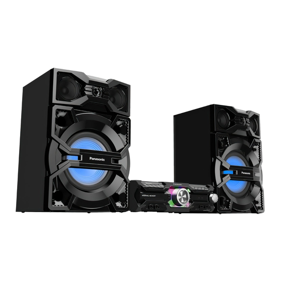
SA-MAX3500PU
Model No.
Product Color: (K)...Black Type
5 Location of Controls and Components------------------ 11
5.1. Remote Control Key Button Operation ------------- 11
5.2. Main Unit Key Button Operation---------------------- 12
6 Service Mode ----------------------------------------------------- 13
6.1. Cold-Start -------------------------------------------------- 13
6.2. Sales Demonstration Lock Function ---------------- 13
6.3. Doctor Mode Table--------------------------------------- 14
6.4. Self-Diagnostic Mode ----------------------------------- 16
6.5. Self-Diagnostic Error Code Table -------------------- 16
7 Troubleshooting Guide --------------------------------------- 18
8 Disassembly and Assembly Instructions--------------- 37
8.1. Types of Screws ----------------------------------------- 37
8.2. Disassembly Flow Chart ------------------------------- 38
8.3. Main Components and P.C.B. Locations----------- 38
8.4. Disassembly of Top Cabinet--------------------------- 39
8.5. Disassembly of Front Panel Unit --------------------- 39
8.6. Disassembly of Button L P.C.B. ---------------------- 40
© Panasonic Corporation 2018. All rights reserved.
Unauthorized copying and distribution is a violation
of law.
PSG1803009CE
CD Stereo System
PAGE
Advertisement
Table of Contents

Related Manuals for Panasonic SA-MAX3500PU


Summary of Contents for Panasonic SA-MAX3500PU
-
Page 1: Table Of Contents
3.1. Service Information --------------------------------------- 9 8.5. Disassembly of Front Panel Unit --------------------- 39 4 Specifications ----------------------------------------------------10 8.6. Disassembly of Button L P.C.B. ---------------------- 40 © Panasonic Corporation 2018. All rights reserved. Unauthorized copying and distribution is a violation of law. - Page 2 8.7. Disassembly of Button R P.C.B. ---------------------- 40 8.8. Disassembly of Panel P.C.B. -------------------------- 41 8.9. Disassembly of USB P.C.B. --------------------------- 41 8.10. Disassembly of Mic P.C.B. ----------------------------- 42 8.11. Disassembly of Tuner P.C.B. -------------------------- 42 8.12. Disassembly of Main P.C.B. --------------------------- 42 8.13.
-
Page 3: Safety Precautions
1 Safety Precautions 1.1. General Guidelines 1. IMPORTANT SAFETY NOTICE There are special components used in this equipment which are important for safety. These parts are marked by in the Schematic Diagrams, Circuit Board Layout, Exploded Views and Replacement Parts List. It is essential that these critical parts should be replaced with manufacturer’s specified parts to prevent X-RADIATION, shock, fire, or other hazards. -
Page 4: Before Repair And Adjustment
1.2. Before Repair and Adjustment Disconnect AC power to discharge AC capacitor (in SMPS P.C.B.) as indicate below diagram through a 10 Ω, 10 W resistor to ground. Figure 1-2 Caution: DO NOT SHORT-CIRCUIT DIRECTLY (with a screwdriver blade, for instance), as this may destroy solid state devices. After repairs are completed, restore power gradually using a variac to avoid overcurrent. -
Page 5: Safety Parts Information
1.4. Safety Parts Information Safety Parts List: There are special components used in this equipment which are important for safety. These parts are marked by in the Schematic Diagrams, Exploded View & Replacement Parts List. It is essential that these critical parts should be replaced with manufacturer’s specified parts to prevent shock, fire or other hazards. -
Page 6: Warning
2 Warning 2.1. Prevention of Electrostatic Discharge (ESD) to Electrostatically Sensi- tive (ES) Devices Some semiconductor (solid state) devices can be damaged easily by static electricity. Such components commonly are called Elec- trostatically Sensitive (ES) Devices. The following techniques should be used to help reduce the incidence of component damage caused by electrostatic discharge (ESD). -
Page 7: General Description About Lead Free Solder (Pbf)
Figure 2-1 2.3. General description about Lead Free Solder (PbF) The lead free solder has been used in the mounting process of all electrical components on the printed circuit boards used for this equipment in considering the globally environmental conservation. The normal solder is the alloy of tin (Sn) and lead (Pb). -
Page 8: Grounding For Electrostatic Breakdown Prevention
4. The antistatic FFC is connected to the new optical pickup unit. After replacing the optical pickup unit and connecting the flexi- ble cable, cut off the antistatic FFC. Figure 2-2 2.5. Grounding for electrostatic breakdown prevention • As for parts that use optical pick-up (laser diode), the optical pick-up is destroyed by the static electricity of the working environ- ment. -
Page 9: Service Navigation
If the circuit is changed or modified, this information will be followed by supplement service manual to be filed with original service manual. 3.1.1. Software Update Panasonic may release updated software for this system that may add or improve the way a feature operates. For more details, refer to the following website. http://panasonic.jp/support/global/cs/... -
Page 10: Specifications
2. Total harmonic distortion is measured by the digital spectrum analyzer. Supported profiles A2DP, AVRCP, SPP, OPP, FTP System: SC-MAX3500PU Operating frequency 2.4 GHz band FH-SS Main Unit: SA-MAX3500PU Speakers: SB-MAX3500PU Frequency band 2402 MHz to 2480 MHz Maximum power (EIRP) 4 dBm Operation distance... -
Page 11: Location Of Controls And Components
5 Location of Controls and Components 5.1. Remote Control Key Button Operation... -
Page 12: Main Unit Key Button Operation
5.2. Main Unit Key Button Operation SELECT SOUND SELECT SOUND KARAOKE MIC VOL... -
Page 13: Service Mode
6 Service Mode 6.1. Cold-Start Item Key Operation FL Display Mode Name Description Front Key Cold Start To carry out cold-start or initialize 1. Unplug AC power cord. to shipping mode 2. Press & hold [ /I] button on main unit. 3. -
Page 14: Doctor Mode Table
6.3. Doctor Mode Table 6.3.1. Doctor Mode Table 1 Item Key Operation FL Display Mode Name Description Front Key Doctor Mode To enter into Doctor Mode In CD Mode: 1. Press [ ] button on main unit follow by [4] and [7] on remote control. - Page 15 6.3.2. Doctor Mode Table 2 Item Key Operation FL Display Mode Name Description Front Key Volume Setting To check volume setting of the main In Doctor Mode: Check unit. 1. Press [7], [8], [9] button on the remote control. Press [7]: VOL50 Volume Press [8]: VOL35 Press [9]: VOL0...
-
Page 16: Self-Diagnostic Mode
6.4. Self-Diagnostic Mode Key Operation Item FL Display Mode Name Description Front Key Self Diagnostic c i t Mode (Ensure no disc is inserted). Step 2: Press & hold [ ] button follow by [ ] on main unit for 2 seconds. Error Code System will perform a check on c i t... - Page 17 6.5.2. CD Mechanism Error Code Table Item Key Operation Solution FL Display (PCB exchange repair) Mode Name Description Front Key Error Code Diagnosis Contents: Press [ ] on main unit Check following: CD H15 for next error. CD Open Abnormal 1.
-
Page 18: Troubleshooting Guide
7 Troubleshooting Guide 7.1. No Power ( No LED Display + No Response) Press Power Button of Unit or Remote Control to Turn ON the Unit No Display on FL Panel Check diode Change D1702 Measured SMPS Check Fuse +18V r more Change (F1001, F1401, SMPS... - Page 19 Check Point SMPS PCB Check Point Main PCB...
- Page 20 7.2. No Sound Coming out from All Speakers Press Power Button of Unit or Remote Control to Turn ON the Unit No Audio in both high and low channel at All Selector - Change series Check DAMP resistors IC PWM input Between DSP Check SOC(IC1001) and DAMP if...
- Page 21 Check Point Main PCB...
- Page 22 7.3. No Sound at USB selector Only Press Power Button of Unit or Remote Control to Turn ON the Unit Select USB A or USB B selector, connect USB device, play source. No Sound comes out from speaker Check IC1202 Change: pin28(USB-A) or pin27(USB-B)
- Page 23 Check Point Main PCB...
- Page 24 7.4. No Sound from MIC at any selector Press Power Button of Unit or Remote Control to Turn ON the Unit Select USB A selector, connect MIC1/ MIC2. Turn ON MIC and speak into MIC. No Sound comes out from speaker. Check SOC Change IC1001...
- Page 25 Check Point MIC pcb: JK140 JK140 IC140 IC140 CN140 Check Point Main PCB C140...
- Page 26 7.5. No Sound in Tuner Mode Press Power Button of Unit or Remote Control to Turn ON the Unit Switch to Tuner (FM Mode) Check I2S Change lines status. IC52 on tuner PCB Check if antenna is R51/52/60 Change connected properly antenna wire connection to Tuner jack.
- Page 27 Check Point Tuner PCB Antenna Check Point Main PCB...
- Page 28 7.6. No Sound in Aux Mode Press Power Button of Unit or Remote Control to Turn ON the Unit Switch to AUX Mode Check I2S Change lines status. IC52 on Tuner PCB R51/52/60 Check if AUX cable is Change connected properly to accessory connection the other player...
- Page 29 Check Point Tuner PCB Antenna Check Point Main PCB...
- Page 30 7.7. FL Show “No Play” at USB selector Only Press Power Button of Unit or Remote Control to Turn ON the Unit Select USB A or USB B selector, connect USB device, TOC reading OK, Press Play , Play Check 3.3V at Check 5V Supply Pin 4 of Replace...
- Page 31 Check Point Main PCB...
- Page 32 7.8. FL Show “No Device” at USB selector Only Press Power Button of Unit or Remote Control to Turn ON the Unit Select USB A or USB B selector, connect USB device, No TOC Check 3.3V at Check 5V Supply Pin 4 of Replace at IC9002(USB...
- Page 33 Check Point Main PCB...
- Page 34 7.9. FL Show “No Play” at Memory selector Only Press Power Button of Unit or Remote Control to Turn ON the Unit Select Memory selector. Ensure that Memory has music track. Press Play , Play . Check 3.3V Supply at Replace LB2001 LB2001 (open)
- Page 35 Check Point Main PCB...
- Page 36 7.10. Bluetooth Pairing Failure Turn ON the Unit Press [ PAIRING] on the Set or Remote Control Display " BLUETOOTH" Do the Cold Start Blinking "PAIRING' will AC Plug-out. Press display, during and Hold "Power" Pairing check/select on button on smartphone or other Main set then ac devices the "EUT"...
-
Page 37: Disassembly And Assembly Instructions
8 Disassembly and Assembly Instructions Caution Note: • This section describes the disassembly and/or assembly procedures for all major printed circuit boards & main compo- nents for the unit. (You may refer to the section of “Main components and P.C.B Locations” as described in the service manual) •... -
Page 38: Disassembly Flow Chart
8.2. Disassembly Flow Chart Top Cabinet Front Panel Unit Tuner P.C.B. Button L P.C.B. Button R P.C.B. Mic P.C.B. Panel P.C.B. Main P.C.B. USB P.C.B. SMPS P.C.B. CD Interface P.C.B. CD Mechanism Unit 8.3. Main Components and P.C.B. Locations... -
Page 39: Disassembly Of Top Cabinet
8.4. Disassembly of Top Cabinet 8.5. Disassembly of Front Panel Unit Step 1 Remove 5 screws. • Refer to “Disassembly of Top Cabinet”. Step 1 Detach 6P Cable at connector (P1803) on Main P.C.B.. Step 2 Detach 22P FFC at connector (P1802) on Main P.C.B.. Step 3 Detach 9P Cable at connector (P1811) on Main P.C.B.. -
Page 40: Disassembly Of Button L P.c.b
8.6. Disassembly of Button L P.C.B. 8.7. Disassembly of Button R P.C.B. • Refer to “Disassembly of Top Cabinet”. • Refer to “Disassembly of Top Cabinet”. • Refer to “Disassembly of Front Panel Unit”. • Refer to “Disassembly of Front Panel Unit”. Step 1 Remove 3 screws. -
Page 41: Disassembly Of Panel P.c.b
8.8. Disassembly of Panel P.C.B. 8.9. Disassembly of USB P.C.B. • Refer to “Disassembly of Top Cabinet”. • Refer to “Disassembly of Top Cabinet”. • Refer to “Disassembly of Front Panel Unit”. • Refer to “Disassembly of Front Panel Unit”. •... -
Page 42: Disassembly Of Mic P.c.b
8.10. Disassembly of Mic P.C.B. 8.12. Disassembly of Main P.C.B. • Refer to “Disassembly of Top Cabinet”. • Refer to “Disassembly of Top Cabinet”. • Refer to “Disassembly of Front Panel Unit”. • Refer to “Disassembly of Front Panel Unit”. Step 1 Remove 2 screws. -
Page 43: Disassembly Of Smps P.c.b
Step 8 Remove 4 screws. 8.13. Disassembly of SMPS P.C.B. Step 9 Release catch. • Refer to “Disassembly of Top Cabinet”. Step 10 Remove Main P.C.B.. • Refer to “Disassembly of Front Panel Unit”. Step 1 Remove screw. Step 2 Detach 13P Cable at connector (CN1851) on SMPS P.C.B.. -
Page 44: Disassembly Of Cd Mechanism Unit
8.14. Disassembly of CD Mecha- 8.15. Disassembly of CD Interface nism Unit P.C.B. • Refer to “Disassembly of Top Cabinet”. • Refer to “Disassembly of Top Cabinet”. • Refer to “Disassembly of Front Panel Unit”. • Refer to “Disassembly of Front Panel Unit”. •... -
Page 45: Service Position
9 Service Position Note: For description of the disassembly procedures, see the Section 8. 9.1. Checking of Panel, Main and SMPS P.C.B. Step 1 Place all P.C.B. on the insulated material as shown. Step 2 Attach 10P FFC at connector (P1806) on Main P.C.B.. Step 3 Attach 10P FFC at connector (P5001) on Main P.C.B.. -
Page 47: Block Diagram
(PLAY) USB1_D+ P1811 CN6901 BT_UART_RX USB1_DP 3 USB_A_D+ BT_UART_TX BLUETOOTH JK6902 FREQUENCY HOST WAKE BT_HOST_WAKE DEVICE BT_UART_RTS 1 USB5V USB PORT B USB0_D- P1811 CN6901 LDO ON R BT_UART_CTS USB0_DM 97 USB_B_D- (REC/PLAY) USB0_D+ P1811 CN6901 USB0_DP 98 USB_B_D+ SA-MAX3500PU... - Page 48 SWITCH Y0/TEMP_DET +5.4V P1501 P1501 QR8501 P1501 PWM_X0 RED_LED LED DRIVE X0/LED_R QR8502 GREEN_LED PWM_X2 X2/LED_B LED DRIVE QR8503 BLUE_LED PWM_X1 X1/LED_G LED DRIVE SB-MAX3500 (R) P1502 P1502 QR8505 Q8513 P1502 PWM_Y1 SUBW_LED_SUPPLY P1502 Y1/MPORT_DET LED DRIVE +5.4V SWITCH SA-MAX3500PU...
- Page 49 TEMP_DET Y0/TEMP_DET AM_BP AM_BP USB_B_ OVC USB_OVC POWER_UP POWER_UP FROM/TO From PDET PDET USB_B_PCONT POWER SUPPLY POWER SUPPLY USB_B_PCONT SYNC SYNC USB_A_PCONT USB_A_PCONT SMPS_ID ADIN2_SMPS_ID PCONT P17 7 PCONT NRST NRST DSP_RST DSP_RESET DSP_MUTE DSP_MUTE TO AUDIO TUN_RST TUN_RST SA-MAX3500PU...
-
Page 50: Audio
SYSTEM TUN_INT TUN_INT TUN_INT TUN_INT TUN_INT GCGPO2 18 CONTROL CN51 P1806 TUN_RST TUN_RST TUN_RST TUN_RST TUN_RST JK51 TUN_WCK TUN_WCK CN51 P1806 TUN_WCK TUN_WCK DFS 14 TUN_LRCK G_TUN_BCK G_TUN_BCK CN51 P1806 G_TUN_BCK G_TUN_BCK FM ANT 2 FMI DCLK 17 TUN_BCK SA-MAX3500PU... - Page 51 JK3500 OUT_B SUB WOOFER 5 INPUT_A SW-_2 JK3500 LEFT OUT_A 6 INPUT_B OUT_A L3301 DAMP_RST OUT_C VALID 24 4 /RST D3000 OUT_D /FAULT D3001 /OTW OUT_D Q3500 Q3501 Q3502 FROM Q3503 SYSTEM CONTROL DC_DET_AMP DC DETECT DC_DET_AMP +38V CIRCUIT SA-MAX3500PU...
-
Page 52: Power Supply
POWER MODE POWER_MODE CN1851 CN2103 CS2 8 SWITCH POWER_UP SYSTEM D1502 FEEDBACK CONTROL CIRCUIT VB 14 D1503 IC1701 VC2 10 SHUNT REGULATOR D1705 Q1505 IC1501 +38.5V CN1851 CN2103 PW_+38V +38V 11,12,13 11,12,13 SWITCHING POWER SUPPLY D1703 PRIMARY CIRCUIT SECONDARY CIRCUIT SA-MAX3500PU... - Page 53 USB_A_SW5R1V USB_A_SW5R1V 5 VIN VOUT USB_A_PCONT 4 EN IC9002 USB SWITCH 3 FLAG TO/FROM SYSTEM CONTROL USB_B_SW5R1V USB_B_SW5R1V P1811 CN6901 USB_B_SW5R1V USB_B_OVC 3 FLAG VOUT USB_B_PCONT 4 EN IC9003 5 VIN USB SWITCH TUNER P.C.B. PW_CD_3R3V P1806 CN51 +3.3V SA-MAX3500PU...
-
Page 54: Wiring Connection Diagram
(CD MECHANISM UNIT) TO OPTICAL PICKUP UNIT (CD MECHANISM UNIT) P1803 P1811 P1802 MIC P.C.B. CN2104 CN1401 TO FAN UNIT P6200 CN6901 USB P.C.B. PANEL P.C.B. CN6204 CN6203 CN6202 BUTTON R P.C.B. BUTTON L P.C.B. CN6201 SA-MAX3500PU WIRING CONNECTION DIAGRAM... -
Page 55: Schematic Diagram
12 Schematic Diagram 12.1. Schematic Diagram Notes • Voltage and signal line • This schematic diagram may be modified at any time : +B signal line with the development of new technology. : CD signal line Notes: : Mic/Aux/Tuner signal line : Output signal line S6206: Power switch (... -
Page 57: Main (Fan Led) And Main (Bluetooth) Circuit
FAN CONTROL LB2103 CN2104 R2147 A OUT POSITIVE FAN UNIT (INTERNAL) NEGATIVE R2153 LB2104 A-IN B OUT Q2111 470K B1ABCF000231 A+IN B-IN Q2110 FAN CONTROL C2129 B1ABCF000231 B+IN FAN CONTROL R2154 C2130 R2152 10V22 R2150 FAN_OUT DC_DET_FAN MGND PW_SW15R0V SA-MAX3500PU... -
Page 58: Main (Fe) Circuit
FA: MAIN (FAN LED) & MAIN (BLUETOOTH CONNECT): SCHEMATIC DIAGRAM - 1 IO: MAIN (IO EXPANSION): SCHEMATIC DIAGRAM - 3 ~ 4 MI: MAIN (MICON): SCHEMATIC DIAGRAM - 5 ~ 7 VR: MAIN (VREG FAN): SCHEMATIC DIAGRAM - 8 ~ 9 DA: MAIN (DAMP): SCHEMATIC DIAGRAM - 10 ~ 12 SA-MAX3500PU... -
Page 59: Main (Io Expansion) Circuit (1/2)
FA: MAIN (FAN LED) & MAIN (BLUETOOTH CONNECT): SCHEMATIC DIAGRAM - 1 FE: MAIN (FE): SCHEMATIC DIAGRAM - 2 MI: MAIN (MICON): SCHEMATIC DIAGRAM - 5 ~ 7 VR: MAIN (VREG FAN): SCHEMATIC DIAGRAM - 8 ~ 9 DA: MAIN (DAMP): SCHEMATIC DIAGRAM - 10 ~ 12 SA-MAX3500PU... -
Page 60: Main (Io Expansion) Circuit (2/2)
FA: MAIN (FAN LED) & MAIN (BLUETOOTH CONNECT): SCHEMATIC DIAGRAM - 1 FE: MAIN (FE): SCHEMATIC DIAGRAM - 2 MI: MAIN (MICON): SCHEMATIC DIAGRAM - 5 ~ 7 VR: MAIN (VREG FAN): SCHEMATIC DIAGRAM - 8 ~ 9 DA: MAIN (DAMP): SCHEMATIC DIAGRAM - 10 ~ 12 SA-MAX3500PU... -
Page 61: Main (Micon) Circuit (1/3)
FA: MAIN (FAN LED) & MAIN (BLUETOOTH CONNECT): SCHEMATIC DIAGRAM - 1 FE: MAIN (FE): SCHEMATIC DIAGRAM - 2 IO: MAIN (IO EXPANSION): SCHEMATIC DIAGRAM - 3 ~ 4 VR: MAIN (VREG FAN): SCHEMATIC DIAGRAM - 8 ~ 9 DA: MAIN (DAMP): SCHEMATIC DIAGRAM - 10 ~ 12 SA-MAX3500PU... -
Page 62: Main (Micon) Circuit (2/3)
DA: MAIN (DAMP): SCHEMATIC DIAGRAM - 10 ~ 12 R1107 180K R1015 VOUT CD Q1001 B1ABCF000176 IC1002 SWITCH PWM_X2 C0EBY0000664 PWM_X1 VOLTAGE DETECTOR J0JCC0000286 PWM_X0 GND VIN LB1028 PWM_Y1 LB1029 PWM_Y0 J0JCC0000286 C1041 FL_SDO LD_CW FL_SCLK FL1_CS LD_CCW SP_CLK SP_DAT RX1010 J0JBD0000050 BT_UART_RTS BT_UART_RX BT_UART_TX SA-MAX3500PU... -
Page 63: Main (Micon) Circuit (3/3)
NRST NRST VDDI VDDI NRST C2008 C2006 R2005 IC2001 EMMC_NRST TZSM12002 NRST DAT7 4GB NAND FLASH MEMORY DAT6 DAT5 DAT4 EMMC_DAT3 DAT3 C2007 C2004 EMMC_DAT2 VSSQ DAT2 EMMC_DAT1 VSSQ DAT1 EMMC_DAT0 C2013 DAT0 [161] CMD VCCQ DAT3 EMMC_CMD R2002 SA-MAX3500PU... -
Page 64: Main (Vreg Fan) Circuit (1/2)
FA: MAIN (FAN LED) & MAIN (BLUETOOTH CONNECT): SCHEMATIC DIAGRAM - 1 FE: MAIN (FE): SCHEMATIC DIAGRAM - 2 IO: MAIN (IO EXPANSION): SCHEMATIC DIAGRAM - 3 ~ 4 MI: MAIN (MICON): SCHEMATIC DIAGRAM - 5 ~ 7 DA: MAIN (DAMP): SCHEMATIC DIAGRAM - 10 ~ 12 SA-MAX3500PU... -
Page 65: Main (Vreg Fan) Circuit (2/2)
FA: MAIN (FAN LED) & MAIN (BLUETOOTH CONNECT): SCHEMATIC DIAGRAM - 1 FE: MAIN (FE): SCHEMATIC DIAGRAM - 2 IO: MAIN (IO EXPANSION): SCHEMATIC DIAGRAM - 3 ~ 4 MI: MAIN (MICON): SCHEMATIC DIAGRAM - 5 ~ 7 DA: MAIN (DAMP): SCHEMATIC DIAGRAM - 10 ~ 12 SA-MAX3500PU... -
Page 66: Main (Damp) Circuit (1/3)
R4010 +PWM2 SDIN2 IC4001 PWM2A R4108 R4009 -PWM2 DSP_SD00 SDIN1 VUEALLPT090 PWM2B R4109 R4008 [12] DVSSCORE +PWM1 DSP_WCK LRCK PWM1A R4110 C4002 R4007 -PWM1 G_DSP_BCK PWM1B DVDD1 REG15 22 23 C4001 LB4003 100P J0JBC0000010 DAMP_RST C4003 C4024 0.01 DC_DET_AMP SA-MAX3500PU... -
Page 67: Main (Damp) Circuit (2/3)
R3512 100K AVDD OUT_C L3101 INPUT_C PVDD_CD G0C100M00013 C3119 INPUT_D PVDD_CD R3104 /FAULT PVDD_CD R3515 R3113 R3513 /OTW OUT_D 100K /CLIP OUT_D C3530 0.01 R3546 C3122 0.033 C3531 0.01 BST_C R3514 GVDD_CD BST_D R3516 100K R3105 C3123 C3106 0.033 SA-MAX3500PU... -
Page 68: Main (Damp) Circuit (3/3)
R3319 C3304 -PWM4 INPUT_B OUT_A 100P C_START PVDD_AB C3305 DVDD PVDD_AB PVDD_AB OUT_B C3306 AVDD OUT_C INPUT_C PVDD_CD R3307 PVDD_CD INPUT_D /FAULT PVDD_CD /OTW OUT_D R3115 /CLIP OUT_D C3326 L3301 0.033 R3311 G0C100M00013 BST_C BST_D C3548 GVDD_CD C3327 0.033 SA-MAX3500PU... -
Page 69: Tuner Circuit
VUEALLPT091 I2C_SDA FM ANT 16 17 18 19 MAIN (IO EXPANSION) FM RADIO RECEIVER TUN_SD0 G1CR18JA0020 CIRCUIT (P1806) LB52 VA51 TUN_WCK LB51 J0JYC0000118 IN SCHEMATIC J0JYC0000656 J0ZZB0000202 G_TUN_BCK DIAGRAM - 3 TUN_INT DOUT THERMAL RFGND C6217 CD3R3_GND PW_CD_3R3V G1C1R0MA0204 SA-MAX3500PU... -
Page 70: Panel Circuit
KEY1_1 KEY1_1 BUTTON R KEY1_2 KEY1_2 CIRCUIT (CN6202) KEY2_1 KEY2_1 IN SCHEMATIC DGND DGND DIAGRAM - 17 CN6204 VR6201 VR6202 KEY1_1 MULTI CONTROL KEY1_1 BUTTON L KEY1_2 KEY1_2 CIRCUIT (CN6201) KEY1 KEY1 IN SCHEMATIC DGND DGND DIAGRAM - 17 SA-MAX3500PU... -
Page 71: Panel (Fl) Circuit
Q6302 B1HFCDE00002 SWITCH C6301 DGND PA: PANEL: SCHEMATIC DIAGRAM - 14 IL: PANEL (ILLUMINATION): SCHEMATIC DIAGRAM - 16 R6330 C6330 C6331 R6326 R6325 REM_IN PW_STBY3R3V IR6301 REMOTE SENSOR FL_GND PW_SW3R3V PW_SW5V PW_FL12V FL_GND FL_GND FL1_CS FL_GND FL_CLK FL_DIN FL_GND SA-MAX3500PU... -
Page 72: Panel (Illumination) Circuit
QR6005 B1GBCFGG0030 R6013 LED DRIVE R6006 QR6013 QR6006 B1GBCFGG0030 B1GBCFGG0030 LED DRIVE LED DRIVE D6009 D6007 D6012 D6010 B3AAA0001246 B3ABA000097 B3AAA0001246 B3ABA000097 R6009 LED3 LED9 QR6010 B1GBCFGG0030 LED DRIVE QR6009 B1GBCFGG0030 C6002 LED DRIVE QR6012 B1GBCFGG0030 LED DRIVE C6001 SA-MAX3500PU... -
Page 73: Button R, Button L, Usb And Cd Interface Circuit
USB PORT B USB_B_D- (REC/PLAY) USBLED_B USB_B_D+ USBLED_A M7301 DGND USB_A_SW5R1V TRAVERSE MOTOR USB_B_SW5R1V D6901 R6909 B3AAA0001243 CN6901 MAIN (IO EXPANSION) DGND_USB R6910 D6902 CIRCUIT (P1811) DGND B3AAA0001243 USB_A_SW5R1V USB_A_SW5R1V IN SCHEMATIC USB_B_SW5R1V DIAGRAM - 3 USB_B_SW5R1V USBLED_B USBLED_B USBLED_A SA-MAX3500PU USBLED_A... -
Page 74: Mic Circuit
MIC_DET_2 MIC AMPLIFIER MIC_DET_2 MIC_DET_1 IN SCHEMATIC MIC_DET_1 MIC_GND DIAGRAM - 3 MIC 1 MIC_GND PW_FL_SW12V LB1404 R1420 R1408 J0JBC0000019 MIC_DET_2 MIC_DET_1 R1433 C1415 R1410 50V0.1 MIC_GND C1444 R1407 C1411 MIC_IN LB1406 C1416 16V10 0.01 MIC_GND C1412 R1423 16V10 SA-MAX3500PU... -
Page 75: Smps Circuit (1/2)
R1519 PFCC CONTROL SWITCH R1502 ISEN GND ICOMP FREQ 470K IC1501 R1503 C0DBBYY00077 R1245 470K R1243 SWITCHING POWER SUPPLY R1236 680K VSEN R1246 R1504 470K R1511 R1514 R1515 6.8K R1205 C1502 50V100 C1503 C1512 0.033 C1504 R1505 C1509 0.01 SA-MAX3500PU... -
Page 76: Smps Circuit (2/2)
R1708 Q1766 R1703 Q1505 2.7K B1ABCF000176 B3PBA0000579 TEMP DETECT R1709 FEEDBACK R1701 1.5K C1708 R1710 QR1720 0.022 1.8K R1721 B1GBCFLL0037 SWITCH R1716 C1704 R1706 R1711 2.4K Q1701 B3PBA0000579 POWER UP R1724 R1725 R1726 4.7K QR1701 C1721 0.01 B1GBCFLL0037 SA-MAX3500PU SWITCH... -
Page 77: Printed Circuit Board
LB1034 C1049 R2002 C1019 C1002 C1001 R2007 C1023 R2006 C1005 C1006 LB1002 C1004 R1084 C1010 R1083 R1035 R1082 C1015 C3535 C1031 C1012 C1032 C3548 C1035 C1046 R1502 LB1509 R1118 C3534 R1809 C3542 C3543 R5038 R5037 6749-1 6749-1 (SIDE A) SA-MAX3500PU... -
Page 78: Main P.c.b. (Side B)
LB1519 QR8504 LB5005 R1808 C1809 QR8501 LB5002 C1827 R3319 R3318 C5020 C3309 P5002 C3308 C5010 P5001 L3300 C5009 C1834 C1836 C1835 QR8503 P1806 QR8502 Q5001 IC5001 C5012 R1801 C5011 R5010 R1841 R5009 C5016 C5015 6749-1 6749-1 R5016 (SIDE B) SA-MAX3500PU... -
Page 79: Tuner And Panel P.c.b
W6022 W6081 D6010 R6010 W6014 D6302 LB6001 W6017 W6076 W6080 W6013 QR6010 W6012 W6084 D6301 C6305 W6075 R6257 W6009 R6325 QR6015 W6083 P6200 W6007 W6006 D6013 W6003 W6004 R6326 R6015 R6030 R6258 QR6013 D6015 R6013 QR6014 6755-1 6755-1 D6020 SA-MAX3500PU... -
Page 80: Button R, Button L, Usb And Mic P.c.b
C1416 R1410 W6902 R1409 C1445 6758-1 6758-1 C1438 LB1404 R1400 R1408 R1411 LB1406 LB1400 R1405 R1418 C1434 R1435 R1421 W1408 C1411 C1401 C1432 W1409 R1414 C1407 R1413 R1420 R1402 C1408 W1401 R1401 LB1401 C1428 W1404 C1409 PbF 6759-1 6759-1 SA-MAX3500PU... -
Page 81: Smps And Cd Interface P.c.b
ZA1001 Q1766 D1705 R1708 D1703 HEATSINK C1601 R1411 Q1404 ZA1701 HEATSINK C1800 R1701 R5859 D1001 QR1767 C1714 R1703 Q1405 R1757 C1716 Q1765 R1702 C1710 R1852 R1756 C1712 D1205 Q1403 C1701 F1401 R1704 CN1851 Q1702 R1420 QR1601 6791-1 PbF 6791-1 SA-MAX3500PU... -
Page 83: Voltage And Waveform Measurement
STANDBY REF NO. IC1001 MODE PLAY STANDBY IC1001 REF NO. MODE PLAY STANDBY IC1001 REF NO. MODE PLAY STANDBY IC1002 REF NO. MODE PLAY STANDBY IC1202 REF NO. MODE PLAY STANDBY IC1202 REF NO. MODE PLAY STANDBY SA-MAX3500PU MAIN P.C.B. - Page 84 30.1 IC3101 REF NO. MODE PLAY STANDBY REF NO. IC3101 MODE PLAY 19.1 19.1 39.5 39.5 39.5 19.1 19.1 39.5 39.5 39.5 19.1 19.4 STANDBY 19.1 19.1 39.5 39.5 39.5 19.1 19.1 39.5 39.5 39.5 19.1 19.4 SA-MAX3500PU MAIN P.C.B.
- Page 85 REF NO. MODE PLAY 30.1 STANDBY 30.1 REF NO. IC4001 MODE PLAY STANDBY IC4001 REF NO. MODE PLAY STANDBY IC4001 REF NO. MODE PLAY STANDBY IC5001 REF NO. MODE PLAY STANDBY IC5001 REF NO. MODE PLAY STANDBY SA-MAX3500PU MAIN P.C.B.
- Page 86 19.7 39.5 39.4 REF NO. Q8512 Q8513 Q9003/Q1806 Q9004/Q1805 QR1201 MODE PLAY STANDBY REF NO. QR2102 QR2103 QR8501 MODE PLAY STANDBY QR8502 QR8503 QR8504 QR8505 QR9002/QR1804 REF NO. MODE PLAY STANDBY REF NO. QR9003/QR1803 MODE PLAY STANDBY SA-MAX3500PU MAIN P.C.B.
- Page 87 196.8 4.2 STANDBY 16.9 196.8 400 196.8 4.2 Q1505 REF NO. MODE PLAY -28.0 -28.0 17.6 -40.1 STANDBY -28.0 -28.0 17.6 -40.1 REF NO. Q1766 QR1601 QR1701 QR1720 QR1767 MODE PLAY -40.1 -36.9 -40.1 STANDBY -40.1 -36.9 -40.1 SA-MAX3500PU SMPS P.C.B.
-
Page 88: Exploded View And Replacement Parts List
15 Exploded View and Replacement Parts List 15.1. Electrical Replacement Parts List Safety Ref. Part No. Part Name & Qty Remarks Description Safety Ref. Part No. Part Name & Qty Remarks C1017 F2A0J331B035 330uF 6.3V Description C1018 F1H1H104B047 0.1uF C1019 F1H1H104B047 0.1uF PRINTED... - Page 89 Safety Ref. Part No. Part Name & Qty Remarks Safety Ref. Part No. Part Name & Qty Remarks Description Description C1078 F1H1H104B047 0.1uF C2155 F2A1A221B161 220uF C1201 F1G1H101A834 100pF C2164 F1H1A105A113 C1202 F1G1H101A834 100pF C2165 F1H1A105A113 C1203 F1G1H101A834 100pF C2166 F1H1H104B047 0.1uF C1204...
- Page 90 Safety Ref. Part No. Part Name & Qty Remarks Safety Ref. Part No. Part Name & Qty Remarks Description Description C3217 F1H2A1040001 0.1uF 100V C5003 F1J1C106A224 10uF C3218 F1J2A1050002 100V C5004 F1H1H104B047 0.1uF C3219 F1J2A1050002 100V C5007 F1H1H222B047 2200pF C3222 F1H1H333A954 0.033uF 50V C5008...
- Page 91 Safety Ref. Part No. Part Name & Qty Remarks Safety Ref. Part No. Part Name & Qty Remarks Description Description L2102 G1C220M00082 INDUCTOR LB5009 D0GBR00J0004 1/10W L3000 G0C100M00013 INDUCTOR LB5010 D0GBR00J0004 1/10W L3001 G0C100M00013 INDUCTOR LB5011 D0GBR00J0004 1/10W L3003 G1C4R7MA0172 INDUCTOR LB5012 D0GBR00J0004...
- Page 92 Safety Ref. Part No. Part Name & Qty Remarks Safety Ref. Part No. Part Name & Qty Remarks Description Description R1031 D0GB103JA065 1/10W R1836 D0GAR00J0005 1/16W R1032 D0GB103JA065 1/10W R1837 D0GAR00J0005 1/16W R1033 D0GB393JA065 1/10W R1838 D0GAR00J0005 1/16W R1034 D0GB103JA065 1/10W R1839 D0GAR00J0005...
- Page 93 Safety Ref. Part No. Part Name & Qty Remarks Safety Ref. Part No. Part Name & Qty Remarks Description Description R2218 D0GFR00J0005 1/4W R3536 D0GB104JA065 100K 1/10W R2237 D0GB222JA065 2.2K 1/10W R3537 D0GB472JA065 4.7K 1/10W R2245 D0GB102JA065 1/10W R3539 D0GBR00J0004 1/10W R2252 D0GB102JA065...
- Page 94 Safety Ref. Part No. Part Name & Qty Remarks Safety Ref. Part No. Part Name & Qty Remarks Description Description RX1206 D1H81014A042 RESISTOR NETWORK C6311 F1H1H105B027 RX1207 D1H81014A042 RESISTOR NETWORK C6312 F1H1H105B027 RX5001 D1H81034A042 RESISTOR NETWORK C6330 F1H1H105B027 OSCILLATORS C6331 F1H1H105B027 X1001 H0J169500045...
- Page 95 Safety Ref. Part No. Part Name & Qty Remarks Safety Ref. Part No. Part Name & Qty Remarks Description Description R6253 D0GB123JA065 1/10W W6055 D0GFR00J0005 1/4W R6254 D0GBR00J0004 1/10W W6056 D0GFR00J0005 1/4W R6255 D0GBR00J0004 1/10W W6058 D0GDR00J0004 1/8W R6256 D0GBR00J0004 1/10W W6059 D0GBR00J0004...
- Page 96 Safety Ref. Part No. Part Name & Qty Remarks Safety Ref. Part No. Part Name & Qty Remarks Description Description CAPACITORS R1412 D0GB681JA065 1/10W C6901 F1H1H104B047 0.1uF R1413 D0GB681JA065 1/10W C6903 F1H1H104B047 0.1uF R1414 D0GB101JA065 1/10W CONNECTORS R1415 D0GB682JA065 6.8K 1/10W CN6901 K1YA09000001...
- Page 97 Safety Ref. Part No. Part Name & Qty Remarks Safety Ref. Part No. Part Name & Qty Remarks Description Description C1706 F2A1H1020067 1000uF QR1720 B1GBCFLL0037 TRANSISTOR C1708 F1H1H223B047 0.022uF 50V QR1767 B1GBCFJJ0041 TRANSISTOR C1710 F1J2E1030004 0.01uF 250V RESISTORS C1712 F1J2E1030004 0.01uF 250V R1001 D0GF105JA048...
- Page 98 Safety Ref. Part No. Part Name & Qty Remarks Description R1717 D0GBR00J0004 1/10W R1721 D1BB2402A074 1/10W R1724 D0GD561JA052 1/8W R1725 D0GB472JA065 4.7K 1/10W R1726 D0GB103JA065 1/10W R1755 D1BB1002A073 1/10W R1756 D1BB1002A073 1/10W R1757 D0GD103JA052 1/8W R1758 D1BB8201A074 8.2K 1/10W R1852 D0GB333JA065 1/10W R5859...
-
Page 99: Mechanical Replacement Part List
15.2. Mechanical Replacement Part List Safety Ref. Part No. Part Name & Qty Remarks Description Safety Ref. Part No. Part Name & Qty Remarks TNMX124 4P WIRE (PANEL- Description BUTTON) TTPA0802 FRONT PANEL UNIT CABINET ASS'Y CHASSIS 24-1 TBXA64201 CONTROL BUTTON L L6FAYYYH0352 DC FAN MOTORS 24-2... - Page 100 Safety Ref. Part No. Part Name & Qty Remarks Description RSAX0002 INDOOR ANTENNA K2DAYYY00002 AC PLUG ADAPTOR...
-
Page 101: Exploded View
CN6201 CN6203 (BUTTON L P.C.B.) (MIC P.C.B.) CN1401 P6200 24-6 JK1401 (PANEL P.C.B.) JK1403 DP6300 24-5 24-3 24-1 24-4 CN6202 24-2 (BUTTON R P.C.B.) CN6901 JK6901 JK6902 (USB P.C.B.) SA-MAX3500PU NOTE: " * " PART IS NOT SUPPLIED. CABINET DRAWING... - Page 102 (CD INTERFACE P.C.B.) P1806 (TUNER P.C.B.) JK3500 P1501 P1502 CN51 CN7001 S7201 P5001 P5002 CN2105 CN2103 P1001 (SMPS P.C.B.) (MAIN P.C.B. P1802 WITH DATA) P1803 P1811 CN1851 CN2104 T1501 SA-MAX3500PU NOTE: " * " PART IS NOT SUPPLIED. CABINET DRAWING...
- Page 103 15.3.3. Packaging ACCESSORIES BAG SA-MAX3500 F R O N T V I E W SB-MAX3500 POLYFOAM (BOTTOM LEFT) POLYFOAM (BOTTOM RIGHT) POLYFOAM (TOP LEFT) POLYFOAM (TOP RIGHT) SC-MAX3500PU PACKAGING DRAWING...
- Page 104 MMH1803...