Table of Contents
Advertisement
Quick Links
Please refer to the original service manual for:
CD Mechanism Unit, Order No. PSG1303059AE
Speaker system SB-MAX9000GN/PU, Order No. PSG1602005CE
TABLE OF CONTENTS
1 Safety Precautions----------------------------------------------- 3
1.1. General Guidelines---------------------------------------- 3
1.2. Before Repair and Adjustment ------------------------- 3
1.3. Protection Circuitry ---------------------------------------- 4
1.4. Caution For Fuse Replacement------------------------ 4
1.5. Safety Parts Information -------------------------------- 5
2 Warning -------------------------------------------------------------- 6
to Electrostatically Sensitive (ES) Devices---------- 6
2.2. Precaution of Laser Diode------------------------------- 6
(PbF)---------------------------------------------------------- 7
2.4. Handling Precautions for Traverse Ass'y------------ 7
prevention --------------------------------------------------- 8
3 Service Navigation ----------------------------------------------- 9
PAGE
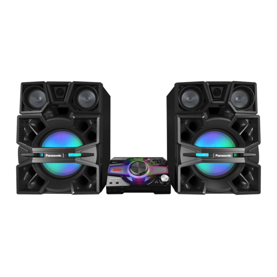
SA-MAX9000GN
Model No.
SA-MAX9000PU
Product Color: (K)...Black Type
3.1. Service Information ----------------------------------------9
3.2. Software Update Procedure-----------------------------9
4 Specifications ---------------------------------------------------- 10
5 Location of Controls and Components------------------ 11
5.1. Remote Control Key Button Operation ------------- 11
5.2. Main Unit Key Button Operation---------------------- 12
6 Service Mode ----------------------------------------------------- 13
6.1. Cold-Start -------------------------------------------------- 13
6.2. Sales Demonstration Lock Function ---------------- 13
6.3. Doctor Mode Table--------------------------------------- 14
6.4. Self-Diagnostic Mode ----------------------------------- 16
6.5. Self-Diagnostic Error Code Table -------------------- 16
7 Troubleshooting Guide --------------------------------------- 18
7.1. No Power or No Display ------------------------------- 18
7.2. Bluetooth® Pairing Failure----------------------------- 18
7.3. No Key Function------------------------------------------ 18
© Panasonic Corporation 2016. All rights reserved.
Unauthorized copying and distribution is a violation
of law.
PSG1602004CE
CD Stereo System
PAGE
Advertisement
Table of Contents

Related Manuals for Panasonic SA-MAX9000GN


Summary of Contents for Panasonic SA-MAX9000GN
-
Page 1: Table Of Contents
7.1. No Power or No Display ------------------------------- 18 prevention --------------------------------------------------- 8 7.2. Bluetooth® Pairing Failure----------------------------- 18 3 Service Navigation ----------------------------------------------- 9 7.3. No Key Function------------------------------------------ 18 © Panasonic Corporation 2016. All rights reserved. Unauthorized copying and distribution is a violation of law. - Page 2 7.4. No Remote Control Function -------------------------- 19 14.1. Voltage Measurement ---------------------------------- 75 7.5. No NFC ----------------------------------------------------- 19 15 Exploded View and Replacement Parts List----------- 81 7.6. USB Device Cannot Detect---------------------------- 19 15.1. Cabinet Parts Location 1------------------------------- 81 7.7. No Output Sound----------------------------------------- 20 15.2.
-
Page 3: Safety Precautions
Disconnect AC power to discharge AC Capacitors (C1003, C1004, C1005, C1007, C1008, C1009, C1010) through a 10 Ω, 10 W resistor to ground. (For SA-MAX9000GN) Disconnect AC power to discharge AC Capacitors (C1001, C1002, C1003, C1004, C1006, C1007, C1008, C1518) through a 10 Ω, 10 W resistor to ground. -
Page 4: Protection Circuitry
1.3. Protection Circuitry The protection circuitry may have operated if either of the following conditions are noticed: • No sound is heard when the power is turned on. • Sound stops during a performance. The function of this circuitry is to prevent circuitry damage if, for example, the positive and negative speaker connection wires are “shorted”, or if speaker systems with an impedance less than the indicated rated impedance of the amplifier are used. -
Page 5: Safety Parts Information
1.5. Safety Parts Information Safety Parts List: There are special components used in this equipment which are important for safety. These parts are marked by in the Schematic Diagrams, Exploded View & Replacement Parts List. It is essential that these critical parts should be replaced with manufacturer’s specified parts to prevent shock, fire or other hazards. -
Page 6: Warning
2 Warning 2.1. Prevention of Electrostatic Discharge (ESD) to Electrostatically Sensi- tive (ES) Devices Some semiconductor (solid state) devices can be damaged easily by static electricity. Such components commonly are called Elec- trostatically Sensitive (ES) Devices. The following techniques should be used to help reduce the incidence of component damage caused by electrostatic discharge (ESD). -
Page 7: General Description About Lead Free Solder (Pbf)
Figure 2-1 2.3. General description about Lead Free Solder (PbF) The lead free solder has been used in the mounting process of all electrical components on the printed circuit boards used for this equipment in considering the globally environmental conservation. The normal solder is the alloy of tin (Sn) and lead (Pb). -
Page 8: Grounding For Electrostatic Breakdown Prevention
ble cable, cut off the antistatic FFC. Figure 2-2 2.5. Grounding for electrostatic breakdown prevention • As for parts that use optical pick-up (laser diode), the optical pick-up is destroyed by the static electricity of the working environ- ment. Repair in the working environment that is grounded. 2.5.1. -
Page 9: Service Navigation
3 Service Navigation 3.1. Service Information This service manual contains technical information which will allow service personnel’s to understand and service this model. Please place orders using the parts list and not the drawing reference numbers. If the circuit is changed or modified, this information will be followed by supplement service manual to be filed with original service manual. -
Page 10: Specifications
Bluetooth 2.1 + EDR Class Class 2 System: SC-MAX9000GN Supported profiles A2DP, AVRCP, SPP, OPP, FTP Main Unit: SA-MAX9000GN Operating frequency 2.4 GHz band FH-SS Speaker System: SB-MAX9000GN Operation distance 10 m line of sight System: SC-MAX9000PU Internal memory section... -
Page 11: Location Of Controls And Components
5 Location of Controls and Components 5.1. Remote Control Key Button Operation... -
Page 12: Main Unit Key Button Operation
5.2. Main Unit Key Button Operation... -
Page 13: Service Mode
6 Service Mode 6.1. Cold-Start Item Key Operation FL Display Mode Name Description Front Key Cold Start To carry out cold-start or initialize 1. Unplug AC power cord. to shipping mode 2. Press & hold [POWER] button. 3. Plug in AC power cord while [POWER] button being pressed. -
Page 14: Doctor Mode Table
6.3. Doctor Mode Table 6.3.1. Doctor Mode Table 1 Item Key Operation FL Display Mode Name Description Front Key Doctor Mode 1. Press [ ] button on main unit follow by [4] and [7] on remote control. 2. To exit, press [ /I] on main unit or remote control EEPROM Displaying of... - Page 15 6.3.2. Doctor Mode Table 2 Item Key Operation FL Display Mode Name Description Front Key Volume Setting To check the volume setting of the In Doctor Mode: Check main unit. 1. Press [7], [8], [9] button on the remote control. Press [7]: VOL50 Volume Press [8]: VOL35...
-
Page 16: Self-Diagnostic Mode
6.4. Self-Diagnostic Mode Item Key Operation FL Display Mode Name Description Front Key Self Diagnostic c i t Mode (Ensure no disc is inserted). Step 2: Press & hold [ ] button follow by [ ] on main unit for 2 seconds. Error Code System will perform a check on c i t... - Page 17 6.5.2. CD Mechanism Error Code Table Item Key Operation Solution FL Display (PCB exchange repair) Mode Name Description Front Key Error Code Diagnosis Contents: Press [ ] on main unit Check following: CD H15 CD Open Abnormal for next error. 1.
-
Page 18: Troubleshooting Guide
7 Troubleshooting Guide 7.1. No Power or No Display Caution: Check Secondary Cap. (C1603) Press Power Button Check Primary E-Cap (C1403) No Display on 1. AC Cord Plug-out or Secondary Diode (D1601) of Unit or Remote Control Measured 200V or more FL Panel 2. -
Page 19: No Remote Control Function
7.4. No Remote Control Function Press Remote Control Press Power Button If Cannot Power Button FL Display Press Remote All Remote Control of the Unit Power ON No Problem Found to Power ON the Unit Show "HELLO" Control Buttons Buttons are Working (No Display) to Turn ON the Set (Ensure have Battery &... -
Page 20: No Output Sound
7.7. No Output Sound CD Play Press Power Button Press Play No Problem Output Sound of Unit or Remote Control CD Mode FL Display "Track & Count" Found to Turn ON the Unit Change CD Mechanism CheckMain PCB & connection Speaker out USB Play Insert USB Thumdrive... -
Page 21: Check Point
7.8. Check Point 7.8.1. SMPS P.C.B. 7.8.2. Main P.C.B. -
Page 22: Disassembly And Assembly Instructions
8 Disassembly and Assembly Instructions • Illustration is based on SA-MAX9000PU. • This section describes the disassembly and/or assembly procedures for all major printed circuit boards & main compo- nents for the unit. (You may refer to the section of “Main components and P.C.B Locations” as described in this service manual) •... -
Page 23: Disassembly Flow Chart
8.2. Disassembly Flow Chart Top Cabinet Front Panel Unit NFC P.C.B. Main P.C.B. USB P.C.B. SMPS P.C.B. Mic P.C.B. CD Mechanism Unit Panel P.C.B CD Interface P.C.B. Tuner P.C.B. -
Page 24: Main Components And P.c.b. Locations
8.3. Main Components and P.C.B. Locations... -
Page 25: Disassembly Of Top Cabinet
8.4. Disassembly of Top Cabinet 8.5. Disassembly of Front Panel Unit Step 1 Remove 2 screws. • Refer to “Disassembly of Top Cabinet”. Step 1 Detach 2P Cable at connector (P8502) on Main P.C.B.. Step 2 Detach 30P FFC at connector (P1802) on Main P.C.B.. Step 3 Detach 12P FFC at connector (P1804) on Main P.C.B.. -
Page 26: Disassembly Of Main P.c.b
Step 6 Release catches. Step 2 Remove 6 screws. Step 7 Remove Front Panel Unit. 8.6. Disassembly of Main P.C.B. • Refer to “Disassembly of Top Cabinet”. • Refer to “Disassembly of Front Panel Unit”. Step 1 Remove 3 screws. -
Page 27: Disassembly Of Smps P.c.b
Step 3 Detach 13P FFC at connector (P9002) on Main P.C.B.. 8.7. Disassembly of SMPS P.C.B. Step 4 Detach 24P FFC at connector (P5002) on Main P.C.B. • Refer to “Disassembly of Top Cabinet”. Step 5 Detach 10P FFC at connector (P5001) on Main P.C.B.. •... -
Page 28: Disassembly Of Cd Mechanism Unit
Step 3 Detach 10P Cable at connector (CN1853) on SMPS 8.8. Disassembly of CD Mecha- P.C.B.. nism Unit Step 4 Detach 13P Cable at connector (CN1851) on SMPS P.C.B.. • Refer to “Disassembly of Top Cabinet”. Step 5 Release catches. •... -
Page 29: Disassembly Of Cd Interface P.c.b
8.9. Disassembly of CD Interface Step 2 Detach 13P FFC at connector (P9003) on Tuner P.C.B.. Step 3 Remove Tuner P.C.B.. P.C.B. • Refer to “Disassembly of Top Cabinet”. • Refer to “Disassembly of Front Panel Unit”. • Refer to “Disassembly of CD Mechanism Unit”. Step 1 Remove 2 screws. -
Page 30: Disassembly Of Usb P.c.b
8.12. Disassembly of USB P.C.B. Step 2 Remove 3 screws. Step 3 Remove Mic P.C.B.. • Refer to “Disassembly of Top Cabinet”. • Refer to “Disassembly of Front Panel Unit”. Step 1 Remove 2 screws. Step 2 Release catches. Step 3 Remove USB P.C.B.. 8.14. - Page 31 Step 3 Remove 4 screws. Step 6 Release catches. Step 4 Remove Fan Unit. Step 7 Remove Panel P.C.B.. Step 5 Remove 15 screws.
-
Page 32: Service Position
9 Service Position 9.2. Checking of SMPS P.C.B. Step 1 Remove Top Cabinet. Note: For description of the disassembly procedures, refer Step 2 Remove Front Panel Unit. Section 8 of the Service Manual. Step 3 Remove SMPS P.C.B.. 9.1. Checking of Panel P.C.B. Step 4 Place SMPS P.C.B. -
Page 33: Checking Of Main P.c.b
9.3. Checking of Main P.C.B. Step 9 Place Main P.C.B., SMPS P.C.B., NFC P.C.B. and Tuner P.C.B. on the insulated material as shown. Step 1 Remove Top Cabinet. Step 10 Attach 2P Cable at connector (P8502) on Main P.C.B.. Step 2 Remove Front Panel Unit. Step 11 Attach 30P FFC at connector (P1802) on Main P.C.B.. -
Page 35: Block Diagram
10 Block Diagram 10.1. System Control... - Page 36 MSDO 24 CIRCUIT FL DATA P1802 P6200 FL DATA MSCLK 23 +3.3V IC2001 4GB NAND FLASH MEMORY DAT1 SD DAT1 DAT3 SD DAT3 DAT3 IR6301 REMOTE SENSOR P1802 P6200 REM IN REM IN +3.3V SA-MAX9000GN/PU SYSTEM CONTROL (2/4) BLOCK DIAGRAM...
- Page 37 X1 30 LED DRIVE LED DRIVE +3.3V QR8503 X2 OUT X2 31 LED DRIVE SB-MAX9000 P1502 P1502 RIGHT TO SYSTEM CONTROL QR8505 Q8513 P1502 BLOCK (4/4) P1502 Y1 OUT Y1 26 LED DRIVE +5.4V SWITCH SA-MAX9000GN/PU SYSTEM CONTROL (3/4) BLOCK DIAGRAM...
- Page 38 SYNC PCONT2 TEMP DET KPY7 PCONT2 TEMP DET ADIN5 PCONT3 FROM/TO PCONT3 PDET KPY6 PDET PDET POWER SUPPLY REG BP REG BP KPX5 NRST NRST DC DET DC DET TO SYSTEM CONTROL BLOCK (3/4) SA-MAX9000GN/PU SYSTEM CONTROL (4/4) BLOCK DIAGRAM...
-
Page 39: Audio
10.2. Audio... - Page 40 RIGHT MID JK4201 D4209 48 CSD Q4208 AMPLIFIER TO AUDIO Q4202 BLOCK (1/2) AMPLIFIER JK4201 LEFT HIGH JK4201 38 IN3 Q4201 AMPLIFIER 40 IN4 44 IN2 Q4203 AMPLIFIER JK4201 46 IN1 LEFT MID JK4201 Q4204 AMPLIFIER SA-MAX9000GN/PU AUDIO (2/2) BLOCK DIAGRAM...
-
Page 41: Power Supply
10.3. Power Supply... - Page 42 FROM/TO SYSTEM CONTROL USB B SW5R1V P9001 CN6002 USB5V USB OVC 3 FLAG VO 1 USB B PCONT 4 EN IC8008 5 VIN USB SWITCH NOTE: “ * ” REF IS FOR INDICATION ONLY SA-MAX9000GN/PU POWER SUPPLY (2/2) BLOCK DIAGRAM...
-
Page 43: Wiring Connection Diagram
TO OPTICAL PICKUP UNIT (CD MECHANISM UNIT) P9001 P5002 NFC P.C.B. P7701 P5001 TO FAN UNIT CN7002 CN1852 P1803 CN7001 USB P.C.B. CD INTERFACE P.C.B. CN6002 TO CD LOADING P.C.B. (CD MECHANISM UNIT) MIC P.C.B. CN1401 P6200 PANEL P.C.B. SA-MAX9000GN/PU WIRING CONNECTION DIAGRAM... -
Page 45: Schematic Diagram
• In case of AC rated voltage Capacitors, the part no. and val- ues will be indicated in the Schematic Diagram. AC rated voltage capacitors: - For SA-MAX9000GN: C1003, C1004, C1005, C1007, C1008, C1009, C1010 - For SA-MAX9000PU: C1001, C1002, C1003, C1004, C1006, C1007, C1008, C1518 •... -
Page 47: Main (Io Expansion) Circuit
DI: MAIN (DIGITAL POWER): SCHEMATIC DIAGRAM - 12 ~ 13 AGND MPORT_GND DIAGRAM - 20 US: MAIN (USB): SCHEMATIC DIAGRAM - 14 MPORT_IN_L AU: MAIN (AUX): SCHEMATIC DIAGRAM - 15 MPORT_IN_L MPORT_DET R1812 R1807 J0JYC0000656 J0JYC0000656 SA-MAX9000GN/PU MAIN (IO EXPANSION) CIRCUIT... -
Page 48: Main (Fan Led) Circuit (1/2)
SE: MAIN (AMP SINGLE): SCHEMATIC DIAGRAM - 9 ~ 10 FE: MAIN (FE): SCHEMATIC DIAGRAM - 11 DI: MAIN (DIGITAL POWER): SCHEMATIC DIAGRAM - 12 ~ 13 US: MAIN (USB): SCHEMATIC DIAGRAM - 14 AU: MAIN (AUX): SCHEMATIC DIAGRAM - 15 SA-MAX9000GN/PU MAIN (FAN LED) CIRCUIT... -
Page 49: Main (Fan Led) Circuit (2/2)
SE: MAIN (AMP SINGLE): SCHEMATIC DIAGRAM - 9 ~ 10 FE: MAIN (FE): SCHEMATIC DIAGRAM - 11 DI: MAIN (DIGITAL POWER): SCHEMATIC DIAGRAM - 12 ~ 13 US: MAIN (USB): SCHEMATIC DIAGRAM - 14 AU: MAIN (AUX): SCHEMATIC DIAGRAM - 15 SA-MAX9000GN/PU MAIN (FAN LED) CIRCUIT... -
Page 50: Main (Dsp) Circuit
FE: MAIN (FE): SCHEMATIC DIAGRAM - 11 C4029 C4028 DI: MAIN (DIGITAL POWER): SCHEMATIC DIAGRAM - 12 ~ 13 US: MAIN (USB): SCHEMATIC DIAGRAM - 14 IC4003 AU: MAIN (AUX): SCHEMATIC DIAGRAM - 15 C0DBCZC00003 VOLTAGE CONVERTER SA-MAX9000GN/PU MAIN (DSP) CIRCUIT... -
Page 51: Main (Amp Btl) Circuit (1/2)
DI: MAIN (DIGITAL POWER): SCHEMATIC DIAGRAM - 12 ~ 13 ZA4501* US: MAIN (USB): SCHEMATIC DIAGRAM - 14 HEATSINK AU: MAIN (AUX): SCHEMATIC DIAGRAM - 15 TO MAIN (AMP BTL) CIRCUIT (2/2) SA-MAX9000GN/PU MAIN (AMP BTL) CIRCUIT NOTE: “ * ” REF IS FOR INDICATION ONLY... -
Page 52: Main (Amp Btl) Circuit (2/2)
120K US: MAIN (USB): SCHEMATIC DIAGRAM - 14 AU: MAIN (AUX): SCHEMATIC DIAGRAM - 15 R4601 R4583 R4596 R4597 R4598 R4599 R4600 R4572 C4549 6.3V47 Q4509 B1HBCDA00001 TO MAIN (AMP BTL) CIRCUIT (1/2) DC DETECT SA-MAX9000GN/PU MAIN (AMP BTL) CIRCUIT... -
Page 53: Main (Micon) Circuit (1/2)
DI: MAIN (DIGITAL POWER): SCHEMATIC DIAGRAM - 12 ~ 13 LB1043 J0JCC0000286 US: MAIN (USB): SCHEMATIC DIAGRAM - 14 PWM_Y2 LB1045 J0JCC0000286 AU: MAIN (AUX): SCHEMATIC DIAGRAM - 15 PWM_Y3 LB1046 J0JCC0000286 PWM_X0 LB1047 J0JCC0000286 PWM_X1 SA-MAX9000GN/PU MAIN (MICON) CIRCUIT NOTE: “ * ” REF IS FOR INDICATION ONLY... -
Page 54: Main (Micon) Circuit (2/2)
21 22 26 27 C1008 LB1001 R1105 C1001 J0JYC0000656 PW_SOC_1R5V C1023 C1051 Q1001 R1106 C1006 X1001 6.3V330 330K H0J169500045 R1025 B1ABCF000176 SWITCH C1027 R1107 180K R1024 LB1040 J0JCC0000286 SA-MAX9000GN/PU MAIN (MICON) CIRCUIT NOTE: “ * ” REF IS FOR INDICATION ONLY... -
Page 55: Main (Amp Single) Circuit (1/2)
SE: MAIN (AMP SINGLE): SCHEMATIC DIAGRAM - 9 ~ 10 FE: MAIN (FE): SCHEMATIC DIAGRAM - 11 DI: MAIN (DIGITAL POWER): SCHEMATIC DIAGRAM - 12 ~ 13 US: MAIN (USB): SCHEMATIC DIAGRAM - 14 AU: MAIN (AUX): SCHEMATIC DIAGRAM - 15 SA-MAX9000GN/PU MAIN (AMP SINGLE) CIRCUIT... -
Page 56: Main (Amp Single) Circuit (2/2)
LEFT LOW- C4236 L4203 G0C100M00015 LEFT LOW+ RIGHT LOW- RIGHT LOW+ Q4203 C4285 DC_DET_AMP B1CBRK000001 1000P AMPLIFIER R4278 120K RIGHT LOW+ Q4209 RIGHT LOW- B1HBCDA00001 R4274 C4282 LEFT LOW+ DC DETECT 6.3V47 DGND LEFT LOW- PW_-40V SA-MAX9000GN/PU MAIN (AMP SINGLE) CIRCUIT... -
Page 57: Main (Fe) Circuit
SE: MAIN (AMP SINGLE): SCHEMATIC DIAGRAM - 9 ~ 10 FE: MAIN (FE): SCHEMATIC DIAGRAM - 11 DI: MAIN (DIGITAL POWER): SCHEMATIC DIAGRAM - 12 ~ 13 US: MAIN (USB): SCHEMATIC DIAGRAM - 14 AU: MAIN (AUX): SCHEMATIC DIAGRAM - 15 SA-MAX9000GN/PU MAIN (FE) CIRCUIT... -
Page 58: Main (Digital Power) Circuit (1/2)
AU: MAIN (AUX): SCHEMATIC DIAGRAM - 15 TEMP_DET SYS5R0V ZC8001* DGND DGND TO MAIN (DIGITAL POWER) FA US BT CIRCUIT (2/2) K8002 R8079 R8078 R8077 R8076 AGND K8005 AMP_GND K8004 MGND K8007 MIC_GND ZJ8003 ZJ8001 ZJ8004 ZJ8005 SA-MAX9000GN/PU MAIN (DIGITAL POWER) CIRCUIT... -
Page 59: Main (Digital Power) Circuit (2/2)
GND_15V FLAG IC8008 C0DBZYY00716 PW_+40V USB SWITCH USB_B_OVC D8011 DA2J10100L USB_B_SW5R1V QR8004 R8058 R8055 B1GBCFJN0038 TO MAIN (DIGITAL POWER) 8.2K QR8005 PCONT CIRCUIT (1/2) B1GDCFGA0018 POWER DETECT C8070 R8059 C8069 R8057 FLAG 120K PW_-40V USB_B_PCONT SA-MAX9000GN/PU MAIN (DIGITAL POWER) CIRCUIT... -
Page 60: Main (Usb) Circuit
SE: MAIN (AMP SINGLE): SCHEMATIC DIAGRAM - 9 ~ 10 FE: MAIN (FE): SCHEMATIC DIAGRAM - 11 DI: MAIN (DIGITAL POWER): SCHEMATIC DIAGRAM - 12 ~ 13 US: MAIN (USB): SCHEMATIC DIAGRAM - 14 AU: MAIN (AUX): SCHEMATIC DIAGRAM - 15 SA-MAX9000GN/PU MAIN (USB) CIRCUIT... -
Page 61: Main (Aux) Circuit
SE: MAIN (AMP SINGLE): SCHEMATIC DIAGRAM - 9 ~ 10 I2C_SDA FE: MAIN (FE): SCHEMATIC DIAGRAM - 11 I2C_SCL DI: MAIN (DIGITAL POWER): SCHEMATIC DIAGRAM - 12 ~ 13 US: MAIN (USB): SCHEMATIC DIAGRAM - 14 TUN_RST AU: MAIN (AUX): SCHEMATIC DIAGRAM - 15 DGND SA-MAX9000GN/PU MAIN (AUX) CIRCUIT... -
Page 62: Tuner Circuit
AGND G2A380Y00002 PW_SW3R3V JK7002 MAIN (AUX) TUN_WCK R7003 R7004 AM ANT 2.7K 2.7K TUN_SDO CIRCUIT (P9002) AM ANT C7002 AM ANT R7012 I2C_SCL IN SCHEMATIC 0.47 R7011 I2C_SDA DIAGRAM - 15 R7005 TUN_RST TUN_INT C7004 G_TUN_BCK DGND SA-MAX9000GN/PU TUNER CIRCUIT... -
Page 63: Panel Circuit (1/3)
R6027 R6026 R6025 QR6032 QR6031 QR6030 QR6029 QR6028 QR6027 QR6026 QR6025 B1GBCFGG0030 B1GBCFGG0030 B1GBCFGG0030 B1GBCFGG0030 B1GBCFGG0030 B1GBCFGG0030 B1GBCFGG0030 B1GBCFGG0030 C6007 C6012 LED DRIVE LED DRIVE LED DRIVE LED DRIVE LED DRIVE LED DRIVE LED DRIVE LED DRIVE SA-MAX9000GN/PU PANEL CIRCUIT... -
Page 64: Panel Circuit (2/3)
B1GBCFGG0030 LED DRIVE LED DRIVE QR6016 QR6009 B1GBCFGG0030 B1GBCFGG0030 LED DRIVE LED DRIVE QR6015 QR6010 B1GBCFGG0030 B1GBCFGG0030 LED DRIVE LED DRIVE QR6014 QR6011 B1GBCFGG0030 B1GBCFGG0030 LED DRIVE LED DRIVE QR6013 QR6012 B1GBCFGG0030 B1GBCFGG0030 LED DRIVE LED DRIVE SA-MAX9000GN/PU PANEL CIRCUIT... -
Page 65: Panel Circuit (3/3)
USB REC MEMORY/USB EFFECT/SAMPLER PW_12V FLGND R6219 R6210 REM_IN 3.3K 3.3K S6220 LOCAL/EQ...GN S6211 LATIN/EQ...PU JUKEBOX R6220 R6211 4.7K 4.7K S6221 S6212 CD/RADIO/AUX R6221 R6212 6.8K 6.8K S6222 S6213 PLAY/PAUSE R6222 R6213 1.2K S6223 S6214 C6002 D.BASS C6001 SA-MAX9000GN/PU PANEL CIRCUIT... -
Page 66: Mic Circuit
MPORT_GND IC1401 DIAGRAM - 1 MPORT_IN_L C1AB00003130 MIC AMPLIFIER MPORT_DET R1420 C1415 R1408 LB1404 50V0.1 J0JBC0000019 R1406 R1407 C1417 100K 1000P JK1402 LB1405 J0JBC0000019 AUX IN 2 LB1406 J0JBC0000019 LB1407 J0JBC0000019 C1421 C1422 C1423 0.01 330P 330P SA-MAX9000GN/PU MIC CIRCUIT... -
Page 67: Usb And Cd Interface Circuit
CN7002 SPM+ SPM- CLOSE_SW REST_SW MAIN (FE) DGND CIRCUIT (P5001) OPEN_SW IN SCHEMATIC LDM- S7201 DIAGRAM - 11 LDM+ RESET TRV- TRV+ M7301* TRAVERSE MOTOR SA-MAX9000GN/PU USB / CD INTERFACE CIRCUIT NOTE: “ * ” REF IS FOR INDICATION ONLY... -
Page 68: Smps Circuit (1/2)
FAN_POSITIVE C1502 25V100 FAN_NEGATIVE IC1701 R1702 2.7K C0DAZYY00039 Q1505 SHUNT REGULATOR B3PBA0000579 R1708 R1703 FEEDBACK R1701 2.7K ZJ1851 1.5K R1709 R1716 C1704 R1710 R1706 R1711 D1701 2.4K DZ2J150M0L SA-MAX9000GN/PU SMPS CIRCUIT NOTE: “ * ” REF IS FOR INDICATION ONLY... -
Page 69: Smps Circuit (2/2)
B0EAMM000057 680K 4700P Q1206 C1408 25V220 B1ABCF000176 R1244 C1404 R1245 SWITCH C1209 R1242 C1405 R1416 R1246 C1214 R1411 R1233 1000P 0.01 C1203 R1412 4700P 470K C1411 C1407 1000P SA-MAX9000GN/PU SMPS CIRCUIT NOTE: “ * ” REF IS FOR INDICATION ONLY... -
Page 70: Printed Circuit Board
LB1014 R1019 LB1001 LB1015 LB1034 LB1004 C1811 R2007 C1021 R2003 C1007 R2006 C1022 LB1803 C1009 R2001 R2002 R2004 LB1007 R1027 R2005 C1028 R1811 C4905 3877AA 3877AA (SIDE A) SA-MAX9000GN/PU NOTE: " * " REF IS FOR INDICATION ONLY MAIN P.C.B. -
Page 71: Main P.c.b. (Side B)
R4905 LB1010 R1823 RX1003 C4910 R1822 RX1004 C8055 IC4901 ZJ8003 P9002 ZJ8005 R1820 C8008 ZJ8006 R1818 R8077 R1817 JK4952 R1816 IC8002 C4907 IC1004 R4909 3877AA 3877AA (SIDE B) NOTE: " * " REF IS FOR INDICATION ONLY SA-MAX9000GN/PU MAIN P.C.B. -
Page 72: Tuner, Mic, Usb And Cd Interface P.c.b
3878AB JK1403 C1423 MIC VOL JK1402 CN7001 AUX IN 2 M7301* TO LOADING P.C.B. (TRAVERSE (CD MECHANISM MOTOR) UNIT) 3556A 3556A NOTE: " * " REF IS FOR INDICATION ONLY SA-MAX9000GN/PU TUNER / MIC / USB / CD INTERFACE P.C.B. -
Page 73: Panel P.c.b
S6207 (DJ2) QR6027 S6210 S6211 QR6026 S6212 (EFFECT/SAMPLER) R6210 (JUKEBOX) QR6030 (DJ6) R6208 R6211 R6201 D6030 D6027 QR6031 QR6032 W6041 R6031 D6031 D6032 S6208 R6027 R6030 (DJ3) S6202 S6209 (OPEN/CLOSE) (ILLUMINATION) 3878AA 3878AA SENSOR MULTI VOLUME CONTROL SA-MAX9000GN/PU PANEL P.C.B. -
Page 74: Smps P.c.b
T500mAL 250V R1416 Q1405 R1603 R1601 R1602 C1407 R1420 IC1402 IC1601 C1853 C1852 C1411 C1403 ZJ1001 Q1404 CN1851 R1607 R1411 Q1702 C1404 ZJ1851 QR1601 Q1403 R1705 3879A 3879A NOTE: " * " REF IS FOR INDICATION ONLY SA-MAX9000GN/PU SMPS P.C.B. -
Page 75: Voltage Measurement
STANDBY IC1001 REF NO. MODE PLAY STANDBY REF NO. IC1001 MODE PLAY STANDBY IC1001 REF NO. MODE PLAY STANDBY IC1002 REF NO. MODE PLAY STANDBY IC1202 REF NO. MODE PLAY STANDBY IC1202 REF NO. MODE PLAY STANDBY SA-MAX9000GN/PU MAIN P.C.B. - Page 76 -36.1 -36.1 -9.9 -1.3 -7.4 -11.5 -7.4 -7.4 -1.3 -9.7 -40.1 -29.6 -40.1 -36.4 -34.9 STANDBY -36.1 -36.1 -9.9 -1.3 -7.4 -11.5 -7.4 -7.4 -1.3 -9.7 -40.1 -29.6 -40.1 -36.4 -34.9 IC4202 REF NO. MODE PLAY -4.6 STANDBY -4.6 SA-MAX9000GN/PU MAIN P.C.B.
- Page 77 11.9 11.9 11.9 STANDBY 11.9 11.9 11.9 IC5001 REF NO. MODE PLAY STANDBY IC5001 REF NO. MODE PLAY STANDBY REF NO. IC7001 MODE PLAY STANDBY IC8001 REF NO. MODE PLAY STANDBY IC8003 REF NO. MODE PLAY STANDBY SA-MAX9000GN/PU MAIN P.C.B.
- Page 78 REF NO. MODE PLAY -10.8 -10.8 -10.8 -10.8 40.1 40.1 40.1 40.1 -10.8 -10.8 -10.8 -10.8 40.1 40.1 40.1 40.1 STANDBY -10.8 -10.8 -10.8 -10.8 40.1 40.1 40.1 40.1 -10.8 -10.8 -10.8 -10.8 40.1 40.1 40.1 40.1 SA-MAX9000GN/PU MAIN P.C.B.
- Page 79 QR8501 QR8502 QR8503 REF NO. MODE PLAY STANDBY QR8504 QR8505 QR8045 QR9002 QR9003 REF NO. MODE PLAY STANDBY SA-MAX9000GN/PU MAIN P.C.B. 14.1.6. Mic and Multi Control P.C.B. IC1401 REF NO. MODE PLAY 11.9 11.9 STANDBY 11.9 11.9 SA-MAX9000GN/PU MIC P.C.B.
- Page 80 REF NO. MODE PLAY 16.9 196.8 400 STANDBY 16.9 196.8 400 Q1502 Q1505 Q1701 Q1702 REF NO. MODE PLAY 196.8 4.2 -28.0 -28.0 17.6 STANDBY 196.8 4.2 -28.0 -28.0 17.6 QR1601 QR1701 REF NO. MODE PLAY STANDBY SA-MAX9000GN/PU SMPS P.C.B.
-
Page 81: Exploded View And Replacement Parts List
15.1. Cabinet Parts Location 1 (NFC P.C.B.) *P7701 (MIC P.C.B.) CN1401 JK1402 JK1403 VR1400 10-3 10-2 10-4 10-5 10-1 10-2 CN6002 JK6001 (USB P.C.B.) JK6002 SA-MAX9000GN/PU NOTE: " * " PART IS NOT SUPPLIED / REF IS FOR INDICATION ONLY. CABINET DRAWING... -
Page 82: Cabinet Parts Location
15.2. Cabinet Parts Location 2 VR6201 IR6301 P6200 DP6300 (PANEL P.C.B.) VR6202 **47 SA-MAX9000GN/PU NOTE: " ** " PART IS FOR SN ONLY. CABINET DRAWING... -
Page 83: Cabinet Parts Location
(CD INTERFACE P.C.B.) F1401 P1001 CN7001 CN1851 F1001 S7201 CN1853 T1501 *HEATSINK F1501 CN1852 (SMPS P.C.B.) *ZC1003 SA-MAX9000GN/PU NOTE: " * " PART IS NOT SUPPLIED / REF IS FOR INDICATION ONLY. " ** " PART IS FOR GN ONLY. CABINET DRAWING... -
Page 84: Packaging
(FOR GN ONLY) AC CORD (FOR PU ONLY) OI BOOK AM LOOP ANTENNA F R O N T SA-MAX9000GN/PU FM INDOOR ANTENNA AC PLUG ADAPTOR (FOR PU ONLY) LEG RUBBER x 8 F R O N T POLYFOAM (BOTTOM LEFT) -
Page 85: Mechanical Replacement Part List
15.5. Mechanical Replacement Part List Safety Ref. Part No. Part Name & Qty Remarks Description RGL0827-Q LIGHT ORNAMENT Safety Ref. Part No. Part Name & Qty Remarks Description RGL0840-Q PATTERN LIGHT PIECE RGR0484A-A REAR PANEL CABINET CHASSIS RGR0484A-D REAR PANEL RGW0450-K MIC KNOB REE1730... - Page 86 Safety Ref. Part No. Part Name & Qty Remarks Description RMN1049-1 FL HOLDER RMN1085-1 IR HOLDER J0KD00000172 FERRITE CORE J0KG00000199 FERRITE CORE XTB3+12JFJK SCREW RXA0277 SMPS SHIELD PLATE UNIT J0KG00000011 FERRITE CORE RSC1341 SHIELD PLATE B TRAVERSE DECK RAE1052Z-V TRAVERSE ASS'Y (E.S.D) XTN2+6GFJ SCREW...
-
Page 87: Electrical Replacement Part List
15.6. Electrical Replacement Part List Safety Ref. Part No. Part Name & Qty Remarks Description IC1402 MIP2F20MSSCF (E.S.D) Safety Ref. Part No. Part Name & Qty Remarks IC1501 C0DBBYY00077 (E.S.D) Description IC1601 C0DAZYY00039 (E.S.D) IC1701 C0DAZYY00039 (E.S.D) PRINTED CIRCUIT IC2001 RFKWNX9000LM (E.S.D) BOARDS... - Page 88 Safety Ref. Part No. Part Name & Qty Remarks Safety Ref. Part No. Part Name & Qty Remarks Description Description Q1206 B1ABCF000176 TRANSISTOR (E.S.D) QR6009 B1GBCFGG0030 TRANSISTOR (E.S.D) Q1402 B1ACKD000006 TRANSISTOR (E.S.D) QR6010 B1GBCFGG0030 TRANSISTOR (E.S.D) Q1403 B3PBA0000579 PHOTO COUPLER (E.S.D) QR6011 B1GBCFGG0030...
- Page 89 Safety Ref. Part No. Part Name & Qty Remarks Safety Ref. Part No. Part Name & Qty Remarks Description Description D4215 B0HCMM000024 DIODE (E.S.D) D4216 B0HCMM000024 DIODE (E.S.D) VARIABLE RESIS- TORS D4217 B0HCMM000024 DIODE (E.S.D) D4501 B0ACGM000002 DIODE (E.S.D) VR1400 EVUE27FK2B53 MIC JOG D4502...
- Page 90 Safety Ref. Part No. Part Name & Qty Remarks Safety Ref. Part No. Part Name & Qty Remarks Description Description L1201 G0C101J00012 INDUCTOR LB1816 J0JYC0000656 INDUCTOR L1202 G0C101J00012 INDUCTOR LB1817 J0JYC0000656 INDUCTOR L4001 G1C100KA0101 INDUCTOR LB2001 J0JYC0000656 INDUCTOR L4002 G1C100KA0101 INDUCTOR LB4001 J0JYC0000656...
- Page 91 Safety Ref. Part No. Part Name & Qty Remarks Safety Ref. Part No. Part Name & Qty Remarks Description Description F1001 K5D103BNA005 FUSE W6018 D0GFR00J0005 1/4W W6019 D0GFR00J0005 1/4W W6020 D0GFR00J0005 1/4W FUSE HOLDERS W6021 D0GBR00J0004 1/10W W6022 D0GFR00J0005 1/4W ZA1002 K3GE1ZZ00001 FUSE HOLDER...
- Page 92 Safety Ref. Part No. Part Name & Qty Remarks Safety Ref. Part No. Part Name & Qty Remarks Description Description W6092 D0GFR00J0005 1/4W R1079 D1BB1502A074 1/10W W6200 D0GFR00J0005 1/4W R1080 D1BB6802A074 1/10W W6201 D0GFR00J0005 1/4W R1081 D0GB103JA065 1/10W W6202 D0GFR00J0005 1/4W R1100 D0GB101JA065...
- Page 93 Safety Ref. Part No. Part Name & Qty Remarks Safety Ref. Part No. Part Name & Qty Remarks Description Description R1423 D0GBR00J0004 1/10W R1821 J0JYC0000656 INDUCTOR R1424 D0GBR00J0004 1/10W R1822 D0GBR00J0004 1/10W R1425 D0GBR00J0004 1/10W R1823 D0GBR00J0004 1/10W R1426 D0GBR00J0004 1/10W R1828 J0JYC0000656...
- Page 94 Safety Ref. Part No. Part Name & Qty Remarks Safety Ref. Part No. Part Name & Qty Remarks Description Description R4201 D0GB100JA065 1/10W R4277 D0GB683JA065 1/10W R4202 D0GB100JA065 1/10W R4278 D0GB124JA065 120K 1/10W R4203 D0GB332JA065 3.3K 1/10W R4289 D0GBR00J0004 1/10W R4204 D0GB151JA065 1/10W...
- Page 95 Safety Ref. Part No. Part Name & Qty Remarks Safety Ref. Part No. Part Name & Qty Remarks Description Description R4568 ERJ14YJ272U 2.7K 1/2W R6013 D0GB101JA065 1/10W R4569 ERJ14YJ100U 1/2W R6014 D0GB820JA065 1/10W R4570 D0GBR00J0004 1/10W R6015 D0GB151JA065 1/10W R4572 D0GB103JA065 1/10W R6016...
- Page 96 Safety Ref. Part No. Part Name & Qty Remarks Safety Ref. Part No. Part Name & Qty Remarks Description Description R6252 D0GB223JA065 1/10W R8503 D0GB681JA065 1/10W R6253 D0GB123JA065 1/10W R8504 D0GBR00J0004 1/10W R6254 D0GBR00J0004 1/10W R8505 D0GB473JA065 1/10W R6255 D0GBR00J0004 1/10W R8506 D0GB123JA065...
- Page 97 Safety Ref. Part No. Part Name & Qty Remarks Safety Ref. Part No. Part Name & Qty Remarks Description Description C1008 F1BAF4710005 470pF C1408 F2A1H1R0A213 1.0uF C1409 F1H1H472B047 4700pF C1008 F1H1H104B047 0.1uF C1411 F1H1H102B047 1000pF C1008 F1BAF1020030 1000pF C1411 F2A1C100A207 10uF C1009 F1H1H104B047...
- Page 98 Safety Ref. Part No. Part Name & Qty Remarks Safety Ref. Part No. Part Name & Qty Remarks Description Description C4005 F1H1H1200004 12pF C4210 F1H1H102B047 1000pF C4006 F1H1H105B027 C4211 F1H1H222B047 2200pF C4007 F1H1H105B027 C4212 F1H1H222B047 2200pF C4008 F1H1H105B027 C4213 F1H1H101B052 100pF C4009 F1H1H102B047...
- Page 99 Safety Ref. Part No. Part Name & Qty Remarks Safety Ref. Part No. Part Name & Qty Remarks Description Description C4505 F1H1H222B047 2200pF C4599 D0GBR00J0004 1/10W C4506 F1H1H102B047 1000pF C4619 F1H1H104B047 0.1uF C4507 F1H1H101B052 100pF C4620 F1H1H104B047 0.1uF C4508 F1J1C106A059 10uF C4904 F1H1H105B027...
- Page 100 Safety Ref. Part No. Part Name & Qty Remarks Description C8002 F1J1C106A059 10uF C8004 F1H1H105B027 C8005 F1H1H105B027 C8006 F1J1A106A043 10uF C8008 F1J1A106A043 10uF C8018 F1H0J1060006 10uF 6.3V C8019 F1H1H105B027 C8023 F1H1H104B047 0.1uF C8024 F1H1H105B027 C8026 F1K1C2260001 22uF C8027 F1K1C2260001 22uF C8029 F1K1E1060009 10uF...