Table of Contents
Advertisement
Please refer to the original service manual for:
CD Mechanism Unit, Mechanism (BRS12C) Order No. PSG1303059AE
Speaker system SB-MAX8000GN, Order No. PSG1502012CE
TABLE OF CONTENTS
1 Safety Precautions----------------------------------------------- 3
1.1. General Guidelines---------------------------------------- 3
1.2. Before Repair and Adjustment ------------------------- 3
1.3. Protection Circuitry ---------------------------------------- 4
1.4. Caution For Fuse Replacement------------------------ 4
1.5. Safety Parts Information -------------------------------- 5
2 Warning -------------------------------------------------------------- 6
to Electrostatically Sensitive (ES) Devices---------- 6
2.2. Precaution of Laser Diode------------------------------- 6
(PbF)---------------------------------------------------------- 7
2.4. Handling Precautions for Traverse Ass'y------------ 7
prevention --------------------------------------------------- 8
3 Service Navigation ----------------------------------------------- 9
PAGE
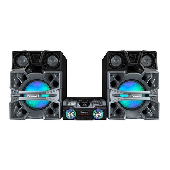
SA-MAX8000GN
Model No.
Product Color: (K)...Black Type
3.1. Service Information ----------------------------------------9
3.2. Software Update Procedure-----------------------------9
4 Specifications ---------------------------------------------------- 10
5 Location of Controls and Components------------------ 11
5.1. Remote Control Key Button Operation ------------- 11
5.2. Main Unit Key Button Operation---------------------- 12
6 Service Mode ----------------------------------------------------- 13
6.1. Cold-Start -------------------------------------------------- 13
6.2. Sales Demonstration Lock Function ---------------- 13
6.3. Doctor Mode Table--------------------------------------- 14
6.4. Self-Diagnostic Mode ----------------------------------- 16
6.5. Self-Diagnostic Error Code Table -------------------- 16
7 Troubleshooting Guide --------------------------------------- 18
8 Disassembly and Assembly Instructions--------------- 19
8.1. Type of Screws ------------------------------------------- 19
8.2. Disassembly Flow Chart ------------------------------- 20
© Panasonic Corporation 2015. All rights reserved.
Unauthorized copying and distribution is a violation
of law.
PSG1502011CE
CD Stereo System
PAGE
Advertisement
Table of Contents

Related Manuals for Panasonic SA-MAX8000GN


Summary of Contents for Panasonic SA-MAX8000GN
-
Page 1: Table Of Contents
8 Disassembly and Assembly Instructions--------------- 19 prevention --------------------------------------------------- 8 8.1. Type of Screws ------------------------------------------- 19 3 Service Navigation ----------------------------------------------- 9 8.2. Disassembly Flow Chart ------------------------------- 20 © Panasonic Corporation 2015. All rights reserved. Unauthorized copying and distribution is a violation of law. - Page 2 8.3. Main Components and P.C.B. Locations ----------- 21 13.3. Illumination Left, Illumination Right and FL Display P.C.B. -------------------------------------------- 72 8.4. Disassembly of Top Cabinet--------------------------- 22 8.5. Disassembly of Fan Unit ------------------------------- 22 13.4. Button Left, Button Right, Mic and USB P.C.B. -- 73 8.6.
-
Page 3: Safety Precautions
1 Safety Precautions 1.1. General Guidelines 1. IMPORTANT SAFETY NOTICE There are special components used in this equipment which are important for safety. These parts are marked by in the Schematic Diagrams, Circuit Board Layout, Exploded Views and Replacement Parts List. It is essential that these critical parts should be replaced with manufacturer’s specified parts to prevent X-RADIATION, shock, fire, or other hazards. -
Page 4: Protection Circuitry
1.3. Protection Circuitry The protection circuitry may have operated if either of the following conditions are noticed: • No sound is heard when the power is turned on. • Sound stops during a performance. The function of this circuitry is to prevent circuitry damage if, for example, the positive and negative speaker connection wires are “shorted”, or if speaker systems with an impedance less than the indicated rated impedance of the amplifier are used. -
Page 5: Safety Parts Information
1.5. Safety Parts Information Safety Parts List: There are special components used in this equipment which are important for safety. These parts are marked by in the Schematic Diagrams, Exploded View & Replacement Parts List. It is essential that these critical parts should be replaced with manufacturer’s specified parts to prevent shock, fire or other hazards. -
Page 6: Warning
2 Warning 2.1. Prevention of Electrostatic Discharge (ESD) to Electrostatically Sensi- tive (ES) Devices Some semiconductor (solid state) devices can be damaged easily by static electricity. Such components commonly are called Elec- trostatically Sensitive (ES) Devices. The following techniques should be used to help reduce the incidence of component damage caused by electrostatic discharge (ESD). -
Page 7: General Description About Lead Free Solder (Pbf)
Figure 2-1 2.3. General description about Lead Free Solder (PbF) The lead free solder has been used in the mounting process of all electrical components on the printed circuit boards used for this equipment in considering the globally environmental conservation. The normal solder is the alloy of tin (Sn) and lead (Pb). -
Page 8: Grounding For Electrostatic Breakdown Prevention
ble cable, cut off the antistatic FFC. Figure 2-2 2.5. Grounding for electrostatic breakdown prevention • As for parts that use optical pick-up (laser diode), the optical pick-up is destroyed by the static electricity of the working environ- ment. Repair in the working environment that is grounded. 2.5.1. -
Page 9: Service Navigation
3 Service Navigation 3.1. Service Information This service manual contains technical information which will allow service personnel’s to understand and service this model. Please place orders using the parts list and not the drawing reference numbers. If the circuit is changed or modified, this information will be followed by supplement service manual to be filed with original service manual. -
Page 10: Specifications
2. Total harmonic distortion is measured by the digital spec- Pick up trum analyzer. Wavelength 790 nm(CD) System: SC-MAX8000GN ® Buetooth section Main Unit: SA-MAX8000GN Speaker System: SB-MAX8000GN Version ® Bluetooth 2.1 + EDR Class Class 2 Supported profiles A2DP, AVRCP, SPP, OPP, FTP Operating frequency 2.4 GHz band FH-SS... -
Page 11: Location Of Controls And Components
5 Location of Controls and Components 5.1. Remote Control Key Button Operation... -
Page 12: Main Unit Key Button Operation
5.2. Main Unit Key Button Operation... -
Page 13: Service Mode
6 Service Mode 6.1. Cold-Start Item Key Operation FL Display Mode Name Description Front Key Cold Start To carry out cold-start or initialize 1. Unplug AC power cord. to shipping mode 2. Press & hold [POWER] button. 3. Plug in AC power cord while [POWER] button being pressed. -
Page 14: Doctor Mode Table
6.3. Doctor Mode Table 6.3.1. Doctor Mode Table 1 Item Key Operation FL Display Mode Name Description Front Key Doctor Mode To enter into Doctor Mode In CD Mode: 1. Press [ ] button on main unit follow by [4] and [7] on remote control. - Page 15 6.3.2. Doctor Mode Table 2 Item Key Operation FL Display Mode Name Description Front Key Volume Setting To check the volume setting of the In Doctor Mode: Check main unit. 1. Press [7], [8], [9] button on the remote control. Press [7]: VOL50 Volume Press [8]: VOL35...
-
Page 16: Self-Diagnostic Mode
6.4. Self-Diagnostic Mode Key Operation Item FL Display Mode Name Description Front Key Self Diagnostic To enter into self diagnostic checking Step 1: Select CD mode Mode (Ensure no disc is inserted). Step 2: Press & hold [ ] button follow by [ ] on main unit for 2 seconds. - Page 17 6.5.2. CD Mechanism Error Code Table Item Key Operation FL Display Mode Name Description Front Key Error Code Diagnosis Contents: Press [ ] on main unit for next CD H15 error. CD Open Abnormal During operation POS_SW_R On fail to be detected within 4 sec. Error No.
-
Page 18: Troubleshooting Guide
7 Troubleshooting Guide "Contents for this section is not available at time of issue"... -
Page 19: Disassembly And Assembly Instructions
8 Disassembly and Assembly Instructions • This section describes the disassembly and/or assembly procedures for all major printed circuit boards & main compo- nents for the unit. (You may refer to the section of “Main components and P.C.B Locations” as described in this service manual) •... -
Page 20: Disassembly Flow Chart
8.2. Disassembly Flow Chart 8.4. Top Cabinet 8.5. Fan Unit 8.6. Front Panel Unit 8.7. FL Display P.C.B. 8.19. SMPS P.C.B. 8.11. Volume Jog P.C.B. 8.8. Illumination Jog 8.12. Illumination Right 8.20. Inner Chassis Unit P.C.B. P.C.B. 8.9. Illumination Left 8.21. -
Page 21: Main Components And P.c.b. Locations
8.3. Main Components and P.C.B. Locations... -
Page 22: Disassembly Of Top Cabinet
8.4. Disassembly of Top Cabinet 8.5. Disassembly of Fan Unit Step 1 Remove 2 screws. • Refer to “Disassembly of Top Cabinet”. Step 1 Detach 2P Wire at connector (CN1852) on SMPS P.C.B.. Step 2 Lift up wire from Fan Holder. Step 2 Remove 5 screws. -
Page 23: Disassembly Of Front Panel Unit
8.6. Disassembly of Front Panel Step 8 Release tabs at bottom of the unit. Unit • Refer to “Disassembly of Top Cabinet”. • Refer to “Disassembly of Fan Unit”. Step 1 Detach 7P Wire at connector (P9002) on Main P.C.B.. Step 2 Detach 14P FFC at connector (P1801) on Main P.C.B.. -
Page 24: Disassembly Of Fl Display P.c.b
8.7. Disassembly of FL Display 8.8. Disassembly Illumination P.C.B. Jog P.C.B. • Refer to “Disassembly of Top Cabinet”. • Refer to “Disassembly of Top Cabinet”. • Refer to “Disassembly of Fan Unit”. • Refer to “Disassembly of Fan Unit”. • Refer to “Disassembly of Front Panel Unit”. •... -
Page 25: Disassembly Of Illumination Left P.c.b
Step 4 Detach 10P FFC at connector (P1930) on Illumination 8.10. Disassembly of BT&NFC P.C.B Jog P.C.B.. • Refer to “Disassembly of Top Cabinet”. Step 5 Detach 6P FFC at connector (P1931) on Illumination • Refer to “Disassembly of Fan Unit”. Jog P.C.B.. -
Page 26: Disassembly Of Illumination Right P.c.b
Step 2 Remove 3 screws. 8.12. Disassembly Illumination Step 3 Release catches. Right P.C.B. • Refer to “Disassembly of Top Cabinet”. • Refer to “Disassembly of Fan Unit”. • Refer to “Disassembly of Front Panel Unit”. • Refer to “Disassembly of Volume Jog P.C.B.”. Step 1 Lift up to remove Illumination Right P.C.B. -
Page 27: Disassembly Of Mic P.c.b
8.14. Disassembly of Mic P.C.B. 8.15. Disassembly of DJ Cabinet • Refer to “Disassembly of Top Cabinet”. Unit • Refer to “Disassembly of Fan Unit”. • Refer to “Disassembly of Top Cabinet”. • Refer to “Disassembly of Front Panel Unit”. •... -
Page 28: Disassembly Of Button Left P.c.b
Step 3 Remove 2 screws. 8.16. Disassembly of Button Left P.C.B. • Refer to “Disassembly of Top Cabinet”. • Refer to “Disassembly of Fan Unit”. • Refer to “Disassembly of Front Panel Unit”. • Refer to “Disassembly of FL Display P.C.B.”. •... -
Page 29: Disassembly Of Multi Control P.c.b
8.17. Disassembly of Multi Control 8.18. Disassembly of Button Right P.C.B. P.C.B. • Refer to “Disassembly of Top Cabinet”. • Refer to “Disassembly of Top Cabinet”. • Refer to “Disassembly of Fan Unit”. • Refer to “Disassembly of Fan Unit”. •... -
Page 30: Disassembly Of Smps P.c.b
8.19. Disassembly of SMPS P.C.B. 8.20. Disassembly of Inner Chassis Unit • Refer to “Disassembly of Top Cabinet”. • Refer to “Disassembly of Fan Unit”. • Refer to “Disassembly of Top Cabinet”. • Refer to “Disassembly of Front Panel Unit”. •... -
Page 31: Disassembly Of Main P.c.b
Step 3 Lift up to remove Inner Chassis Unit. Step 2 Remove 2 screws. Step 3 Detach 2P Wire at connector (P8503) on Main P.C.B.. Step 4 Detach 2P Wire at connector (P8502) on Main P.C.B.. Step 5 Detach 10P FFC at connector (P5001) on Main P.C.B.. Step 6 Detach 24P FFC at connector (P5002) on Main P.C.B.. -
Page 32: Disassembly Of Cd Mechanism Unit
8.22. Disassembly of CD Mecha- 8.23. Disassembly of CD Interface nism Unit P.C.B. • Refer to “Disassembly of Top Cabinet”. • Refer to “Disassembly of Top Cabinet”. • Refer to “Disassembly of Fan Unit”. • Refer to “Disassembly of Fan Unit”. •... -
Page 33: Service Position
9 Service Position Note: For description of the disassembly procedures, refer Step 11 Place FL Display P.C.B. on the insulated material as Section 8 of the Service Manual. shown. Step 12 Attach 13P FFC at connector (P1700) on FL Display 9.1. -
Page 34: Checking Of Smps P.c.b
9.2. Checking of SMPS P.C.B. 9.3. Checking of Main P.C.B. Step 1 Remove Top Cabinet. Step 1 Remove Top Cabinet. Step 2 Remove Front Panel Unit. Step 2 Remove Front Panel Unit. Step 3 Remove Fan Unit. Step 3 Remove Fan Unit. Step 4 Remove SMPS P.C.B.. -
Page 35: Block Diagram
BT UART RTS UART0 RTS P9001 CN9001 D+ A D+ A 2D+ 7 3 USB A D+ P7701* P1504 P1500 P1802 BT LDO ON BT LDO ON NOTE: “ * ” REF IS FOR INDICATION ONLY SA-MAX8000GN SYSTEM CONTROL (1/4) BLOCK DIAGRAM... - Page 36 FL1 CS P1802 P1500 P1502 P1600 P1601 P1700 FL1 CS MSCS 21 +3.3V DAT2 SD DAT2 DAT3 SD DAT3 DAT3 IR1730 REMOTE SENSOR P1802 P1500 P1502 P1600 P1601 P1700 REM IN REM IN +3.3V SA-MAX8000GN SYSTEM CONTROL (2/4) BLOCK DIAGRAM...
- Page 37 Z7 10 D1515, D1512, D1522 D1503 KIRARI IN P1801 P1501 KIRARI IN CLKIO Z8 8 D1505 D1511 D1504 TO SYSTEM CONTROL BLOCK (4/4) D1508 P1801 P1501 Z10 5 D1502 D1500 D1506 P1801 P1501 Z9 6 SA-MAX8000GN SYSTEM CONTROL (3/4) BLOCK DIAGRAM...
- Page 38 USB A PCONT SYNC PX4 23 SYNC GPIO17 TEMP DET TEMP DET ADIN5 PDET +40V PDET +40V GPIO0 FROM/TO PDET PDET GPIO15 POWER SUPPLY NRST NRST DC DET DC DET TO SYSTEM CONTROL BLOCK (3/4) SA-MAX8000GN SYSTEM CONTROL (4/4) BLOCK DIAGRAM...
-
Page 39: Audio
KIRARI IN PWM3A TUN RST FROM/TO TUN RST FROM/TO SYSTEM CONTROL TUN WCK SYSTEM CONTROL TUN WCK DFS 14 TUN BCK TUN BCK DCLK 17 I2C SCL SCLK I2C SCL I2C SDA SDIO I2C SDA SA-MAX8000GN AUDIO (1/2) BLOCK DIAGRAM... - Page 40 RIGHT MID JK4201 D4209 48 CSD Q4208 AMPLIFIER TO AUDIO Q4202 BLOCK (1/2) AMPLIFIER JK4201 LEFT HIGH JK4201 38 IN3 Q4201 AMPLIFIER 40 IN4 44 IN2 Q4203 AMPLIFIER JK4201 46 IN1 LEFT MID JK4201 Q4204 AMPLIFIER SA-MAX8000GN AUDIO (2/2) BLOCK DIAGRAM...
-
Page 41: Power Supply
PW -40V REGULATOR D1705 Q4511 Q1505 D4520 +B (40V) CN1853 P4501 +B (40V) PW -29V PW -29V 1,2,3 1,2,3 -29V SWITCH D1703 D4518 D4521 PRIMARY SECONDARY PW +40V +40V DC DET SYSTEM CONTROL PW +40V SA-MAX8000GN POWER SUPPLY (1/2) BLOCK DIAGRAM... - Page 42 USB B 5R2V P9002 CN9002 USB B 5R2V USB5V USB OVC 3 FLAG VO 1 USB B PCONT 4 EN IC8008 C0DBZYY00716 5 VIN USB SWITCH NOTE: “ * ” REF IS FOR INDICATION ONLY SA-MAX8000GN POWER SUPPLY (2/2) BLOCK DIAGRAM...
-
Page 43: Wiring Connection Diagram
P1930 BUTTON LEFT P.C.B. P1932 P1960 VOLUME JOG P.C.B. P1931 P1961 ILLUMINATION JOG P.C.B. P1503 P1504 P1950 P1980 P7701* ILLUMINATION ILLUMINATION BT&NFC P.C.B RIGHT P.C.B. LEFT P.C.B. NOTE: " * " REF IS FOR INDICATION ONLY. SA-MAX8000GN WIRING CONNECTION DIAGRAM... -
Page 45: Schematic Diagram
12 Schematic Diagram 12.1. Schematic Diagram Notes • Voltage and signal line : +B signal line • This schematic diagram may be modified at any time : -B signal line with the development of new technology. : CD Audio input signal line Notes: : Tuner/AUX/Mic input signal line : Audio output signal line... -
Page 47: Main (Io Expansion) Circuit
R1809 MIC_IN MIC_IN R1828 J0JYC0000656 MIC_DET_2 R1810 J0JYC0000656 MIC_DET_1 MIC CIRCUIT R1806 J0JYC0000656 C1809 1000P (CN1401) MPORT_IN_R MIC_GND MPORT_IN_R IN SCHEMATIC KA DI AGND MPORT_GND DIAGRAM - 20 MPORT_IN_L MPORT_IN_L MPORT_DET R1807 R1812 J0JYC0000656 J0JYC0000656 SA-MAX8000GN MAIN (IO EXPANSION) CIRCUIT... -
Page 48: Main (Fan Led) Circuit
US: MAIN (USB): SCHEMATIC DIAGRAM - 14 Q8510 R8527 C8518 R8529 AU: MAIN (AUX TUNER): SCHEMATIC DIAGRAM - 15 R8526 C8511 10V100 100K B1ABCF000231 R8525 NOTE: “ * ” REF IS FOR INDICATION ONLY FAN LOCK SA-MAX8000GN MAIN (FAN LED) CIRCUIT... -
Page 49: Main (Dsp) Circuit
IC4003 KA: MAIN (KARAOKE): SCHEMATIC DIAGRAM - 11 C0DBCZC00003 DI: MAIN (DIGITAL POWER): SCHEMATIC DIAGRAM - 12 ~ 13 VOLTAGE CONVERTER US: MAIN (USB): SCHEMATIC DIAGRAM - 14 SA-MAX8000GN MAIN (DSP) CIRCUIT AU: MAIN (AUX TUNER): SCHEMATIC DIAGRAM - 15... -
Page 50: Main (Amp Btl) Circuit (1/2)
CIRCUIT (2/2) DI: MAIN (DIGITAL POWER): SCHEMATIC DIAGRAM - 12 ~ 13 US: MAIN (USB): SCHEMATIC DIAGRAM - 14 AU: MAIN (AUX TUNER): SCHEMATIC DIAGRAM - 15 SA-MAX8000GN MAIN (AMP BTL) CIRCUIT NOTE: “ * ” REF IS FOR INDICATION ONLY... -
Page 51: Main (Amp Btl) Circuit (2/2)
AU: MAIN (AUX TUNER): SCHEMATIC DIAGRAM - 15 RL4502* R4601 R4583 R4596 R4597 R4598 R4599 R4600 R4572 C4549 6.3V47 Q4509 B1HBCDA00001 TO MAIN (AMP BTL) CIRCUIT (1/2) DC DETECT SA-MAX8000GN MAIN (AMP BTL) CIRCUIT NOTE: “ * ” REF IS FOR INDICATION ONLY... -
Page 52: Main (Micon) Circuit (1/2)
SSDI VOL_JOG_B DI: MAIN (DIGITAL POWER): SCHEMATIC DIAGRAM - 12 ~ 13 US: MAIN (USB): SCHEMATIC DIAGRAM - 14 AU: MAIN (AUX TUNER): SCHEMATIC DIAGRAM - 15 SA-MAX8000GN MAIN (MICON) CIRCUIT NOTE: “ * ” REF IS FOR INDICATION ONLY... -
Page 53: Main (Micon) Circuit (2/2)
20 21 24 25 26 27 C1008 LB1003 LB1001 C1026 J0JYC0000656 J0JYC0000656 PW_SOC_1R5V C1023 C1040 R1105 R1025 X1001 Q1001 R1106 330K H0J169500045 B1ABCF000176 SWITCH C1027 R1024 NRST SA-MAX8000GN MAIN (MICON) CIRCUIT NOTE: “ * ” REF IS FOR INDICATION ONLY... -
Page 54: Main (Amp Single) Circuit (1/2)
KA: MAIN (KARAOKE): SCHEMATIC DIAGRAM - 11 DI: MAIN (DIGITAL POWER): SCHEMATIC DIAGRAM - 12 ~ 13 US: MAIN (USB): SCHEMATIC DIAGRAM - 14 AU: MAIN (AUX TUNER): SCHEMATIC DIAGRAM - 15 SA-MAX8000GN MAIN (AMP SINGLE) CIRCUIT NOTE: “ * ” REF IS FOR INDICATION ONLY... -
Page 55: Main (Amp Single) Circuit (2/2)
RIGHT LOW+ Q4203 C4285 DC_DET_AMP B1CBRK000001 1000P AMPLIFIER R4278 120K RIGHT LOW+ Q4209 RIGHT LOW- B1HBCDA00001 R4274 C4282 LEFT LOW+ DC DETECT 6.3V47 DGND LEFT LOW- PW_-40V SA-MAX8000GN MAIN (AMP SINGLE) CIRCUIT NOTE: “ * ” REF IS FOR INDICATION ONLY... -
Page 56: Main (Fe) Circuit
FE: MAIN (FE): SCHEMATIC DIAGRAM - 10 KA: MAIN (KARAOKE): SCHEMATIC DIAGRAM - 11 DI: MAIN (DIGITAL POWER): SCHEMATIC DIAGRAM - 12 ~ 13 US: MAIN (USB): SCHEMATIC DIAGRAM - 14 AU: MAIN (AUX TUNER): SCHEMATIC DIAGRAM - 15 SA-MAX8000GN MAIN (FE) CIRCUIT... -
Page 57: Main (Karaoke) Circuit
FE: MAIN (FE): SCHEMATIC DIAGRAM - 10 KA: MAIN (KARAOKE): SCHEMATIC DIAGRAM - 11 DI: MAIN (DIGITAL POWER): SCHEMATIC DIAGRAM - 12 ~ 13 US: MAIN (USB): SCHEMATIC DIAGRAM - 14 AU: MAIN (AUX TUNER): SCHEMATIC DIAGRAM - 15 SA-MAX8000GN MAIN (KARAOKE) CIRCUIT... -
Page 58: Main (Digital Power) Circuit (1/2)
AU: MAIN (AUX TUNER): SCHEMATIC DIAGRAM - 15 SYNC IN SCHEMATIC DIAGRAM - 22 C8052 C8054 25V1000 GND_15V GND_15V GND_15V TEMP_DET SYS5R0V ZC8001* DGND DGND FA US AB R8078 K8002 AGND R8079 ZJ8001 K8005 AMP_GND ZJ8003 K8004 MGND SA-MAX8000GN MAIN (DIGITAL POWER) CIRCUIT... -
Page 59: Main (Digital Power) Circuit (2/2)
CONVERTER IC8008 C0DBZYY00716 PW_+40V USB SWITCH D8011 DA2J10100L USB_B_SW5R1V QR8004 R8058 R8055 B1GBCFJN0038 8.2K D8012 QR8005 PDET_+40V PCONT DZ2J130M0L B1GDCFGA0018 QR8003 POWER DETECT B1GBCFJJ0040 C8070 R8059 C8069 R8057 FLAG 120K R8056 POWER DETECT PW_-40V USB_B_PCONT SA-MAX8000GN MAIN (DIGITAL POWER) CIRCUIT... -
Page 60: Main (Usb) Circuit
FE: MAIN (FE): SCHEMATIC DIAGRAM - 10 KA: MAIN (KARAOKE): SCHEMATIC DIAGRAM - 11 DI: MAIN (DIGITAL POWER): SCHEMATIC DIAGRAM - 12 ~ 13 US: MAIN (USB): SCHEMATIC DIAGRAM - 14 AU: MAIN (AUX TUNER): SCHEMATIC DIAGRAM - 15 SA-MAX8000GN MAIN (USB) CIRCUIT... -
Page 61: Main (Aux Tuner) Circuit
FE: MAIN (FE): SCHEMATIC DIAGRAM - 10 KA: MAIN (KARAOKE): SCHEMATIC DIAGRAM - 11 C7004 DI: MAIN (DIGITAL POWER): SCHEMATIC DIAGRAM - 12 ~ 13 US: MAIN (USB): SCHEMATIC DIAGRAM - 14 DGND AU: MAIN (AUX TUNER): SCHEMATIC DIAGRAM - 15 SA-MAX8000GN MAIN (AUX TUNER) CIRCUIT... -
Page 62: Illumination Left, Illumination Right, Illumination Jog And Volume Jog Circuit
BUTTON LEFT CIRCUIT (P1503) ILLUMI_JOG_B IN SCHEMATIC ILLUMI_JOG_A DIAGRAM - 18 VOL_JOG_B VOL_JOG_A DGND PW_SW3R3V R1931 R1930 C1931 C1930 P1961 100P 100P P1930 PW_SW3R3V DGND VOL_JOG_A VOL_JOG_B SA-MAX8000GN ILLUMINATION LEFT / ILLUMINATION RIGHT / ILLUMINATION JOG / VOLUME JOG CIRCUIT... -
Page 63: Fl Display Circuit
R1800 R1801 C1812 C1806 R1810 R1811 C1807 DGND R1809 R1803 1.2K C1802 C1800 D1802 B0ADDH000009 C1803 R1816 R1813 R1815 2.7K PW_FL12V Q1802 D1801 Q1801 B0ADDH000009 R1814 B1HFCDE00002 B1HFCDE00002 C1804 C1801 4.7K SWITCH SWITCH PGND FL_DATA PW_SW3R3V SA-MAX8000GN FL DISPLAY CIRCUIT... -
Page 64: Button Left Circuit
S1507 S1509 R1532 R1531 R1533 PW5V R1504 3.9K PW_5V PW_SW3R3V R1505 PW_SW3R3V R1507 DGND R1512 DGND PW_STBY3R3V R1508 PW_STBY3R3V REM_IN REM_IN S1512 S1510 S1511 R1536 R1535 R1534 NFC_D3R3V DJ JUKEBOX DJ SAMPLER DJ EFFECT 3.9K 6.8K SA-MAX8000GN BUTTON LEFT CIRCUIT... -
Page 65: Button Right And Multi Control Circuit
R1609 KEY_3 MUX_INPUT_A R1610 KEY_4 MUX_KEY4 R1611 KEY_B MUX_KEY1 R1612 DGND MUX_KEY2 DGND KEY_B DJ_JOG_B R1600 R1601 DJ_JOG_A C1602 C1600 C1601 10V22 100P 100P 1 2 3 IC1600 C0JBAR000655 VR1600 MULTIPLEXER MULTI CONTROL SA-MAX8000GN BUTTON RIGHT / MULTI CONTROL CIRCUIT... -
Page 66: Mic Circuit
MPORT_IN_L MPORT_DET MIC AMPLIFIER R1420 C1415 R1408 LB1404 50V0.1 J0JBC0000019 R1406 R1407 C1417 100K 1000P JK1402 LB1405 J0JBC0000019 AUX IN 2 LB1406 J0JBC0000019 LB1407 J0JBC0000019 C1418 C1419 C1420 C1421 C1422 C1423 0.01 0.01 0.01 0.01 330P 330P SA-MAX8000GN MIC CIRCUIT... -
Page 67: Usb And Cd Interface Circuit
CN7002 SPM+ SPM- CLOSE_SW REST_SW MAIN (FE) DGND CIRCUIT (P5001) OPEN_SW IN SCHEMATIC LDM- S7201 DIAGRAM - 10 LDM+ RESET TRV- TRV+ M7301* TRAVERSE MOTOR SA-MAX8000GN USB / CD INTERFACE CIRCUIT NOTE: “ * ” REF IS FOR INDICATION ONLY... -
Page 68: Smps Circuit (1/2)
ZJ1851 1.5K B1ADNG000003 CHASSIS GND SWITCH C1720 R1709 R1716 0.01 R1722 QR1720 C1704 R1710 R1720 B1GBCFLL0037 D1508 0.033 B0EAMM000057 R1706 SWITCH D1701 R1721 DZ2J150M0L D1507 R1711 B0EAMM000057 2.4K SA-MAX8000GN SMPS CIRCUIT NOTE: “ * ” REF IS FOR INDICATION ONLY... -
Page 69: Smps Circuit (2/2)
POWER SUPPLY CONTROL B0EAMM000057 C1217 C1408 25V220 C1404 C1405 R1416 R1411 1000P IC1202 C0DBBYY00076 R1412 PFC CONTROL 470K C1411 C1407 R1206 R1224 1000P D1206 C1219 C1220 DZ2J051M0L 1000P SA-MAX8000GN SMPS CIRCUIT NOTE: “ * ” REF IS FOR INDICATION ONLY... -
Page 70: Printed Circuit Board
R4261 R4263 R4264 R4262 R1809 R1808 R4583 R8079 R4930 3838AA 3838AA R4834 R4831 R4830 R4829 C7002 R1504 R1506 R1507 R4901 L7001 C4904 R4904 R4902 R4903 LB7001 (SIDE A) NOTE: " * " REF IS FOR INDICATION ONLY SA-MAX8000GN MAIN P.C.B. -
Page 71: Main P.c.b. (Side B)
3-LL+ 5-RM+ 7-RH+ 9-LM+ 11-LH+ P1502 P1501 (TO SB-MAX800) (TO SB-MAX800) 2-RL- 4-LL- 6-RM- 8-RH- 10-LM- 12-LH- TO SPEAKERS AUX IN 1 FM ANT AM ANT (SIDE B) NOTE: " * " REF IS FOR INDICATION ONLY SA-MAX8000GN MAIN P.C.B. -
Page 72: Illumination Left, Illumination Right And Fl Display P.c.b
R1815 R1715 D1701 D1801 C1730 R1730 D1702 D1802 C1712 C1812 C1711 R1704 C1706 R1706 C1707 C1811 R1804 C1806 R1806 C1807 DP1800 R1700 R1800 R1701 R1801 DP1700 ZA1701 IR1730 3839AA 3839AA SA-MAX8000GN ILLUMINATION LEFT / ILLUMINATION RIGHT / FL DISPLAY P.C.B. -
Page 73: Button Left, Button Right, Mic And Usb P.c.b
C1409 R1404 LB1404 K1401 R1408 W4002 R1403 W4000 R1407 K1400 C1417 C1418 LB1405 C1423 C1441 LB1407 C1421 C1420 VR1401 LB1406 C1419 C1422 R1409 JK1402 MIC VOL AUX IN 2 SA-MAX8000GN BUTTON LEFT / BUTTON RIGHT / MIC / USB P.C.B. -
Page 74: Volume Jog, Illumination Jog, Multi Control And Cd Interface P.c.b
IC1600 CN7001 M7301* TO LOADING P.C.B. VR1600 (TRAVERSE (CD MECHANISM MOTOR) UNIT) 3556A 3556A 3839AJ 3839AJ MULTI CONTROL NOTE: " * " REF IS FOR INDICATION ONLY SA-MAX8000GN VOLUME JOG / ILLUMINATION JOG / MULTI CONTROL / CD INTERFACE P.C.B. -
Page 75: Smps P.c.b
D1704 D1706 C1711 R1001 R1002 C1710 C1713 DZ1001 F1001 T10AH 250V ZA1003 ZA1002 C1001 P1001 CN1852 (TO FAN (SMPS)) ZJ1701 K7...MAX8000GN 3840A 3840A AC IN ~ 220V-240V 50Hz NOTE: " * " REF IS FOR INDICATION ONLY SA-MAX8000GN SMPS P.C.B. -
Page 77: Voltage And Waveform Measurement
STANDBY REF NO. IC1001 MODE PLAY STANDBY REF NO. IC1001 MODE PLAY STANDBY IC1001 REF NO. MODE PLAY STANDBY IC1002 REF NO. MODE PLAY STANDBY IC1202 REF NO. MODE PLAY STANDBY IC1202 REF NO. MODE PLAY STANDBY SA-MAX8000GN MAIN P.C.B. - Page 78 -40.1 IC4202 REF NO. MODE PLAY -36.1 -36.1 -9.9 -1.3 -7.4 -11.5 -7.4 -7.4 -1.3 -9.7 -40.1 -29.6 -40.1 -36.4 -34.9 STANDBY -36.1 -36.1 -9.9 -1.3 -7.4 -11.5 -7.4 -7.4 -1.3 -9.7 -40.1 -29.6 -40.1 -36.4 -34.9 SA-MAX8000GN MAIN P.C.B.
- Page 79 STANDBY IC4901 REF NO. MODE PLAY 11.9 11.9 11.9 STANDBY 11.9 11.9 11.9 IC5001 REF NO. MODE PLAY STANDBY IC5001 REF NO. MODE PLAY STANDBY IC7001 REF NO. MODE PLAY STANDBY IC8001 REF NO. MODE PLAY STANDBY SA-MAX8000GN MAIN P.C.B.
- Page 80 REF NO. MODE PLAY -10.8 -10.8 -10.8 -10.8 -10.8 -10.8 -10.8 -10.8 40.1 40.1 40.1 40.1 -10.8 -10.8 -10.8 -10.8 STANDBY -10.8 -10.8 -10.8 -10.8 -10.8 -10.8 -10.8 -10.8 40.1 40.1 40.1 40.1 -10.8 -10.8 -10.8 -10.8 SA-MAX8000GN MAIN P.C.B.
- Page 81 REF NO. MODE PLAY -4.6 -36.2 -36.2 11.9 STANDBY -4.6 -36.2 -36.2 11.9 QR4902 QR8001 QR8003 QR8004 QR8005 REF NO. MODE PLAY 11.9 24.5 -6.6 STANDBY 11.9 24.5 -6.6 QR8045 QR9002 QR9003 REF NO. MODE PLAY STANDBY SA-MAX8000GN MAIN P.C.B.
- Page 82 REF NO. MODE PLAY 11.9 11.9 STANDBY 11.9 11.9 SA-MAX8000GN MIC P.C.B. IC1600 REF NO. MODE PLAY STANDBY SA-MAX8000GN MULTI CONTROL P.C.B. 14.1.7. SMPS P.C.B. REF NO. IC1101 MODE PLAY 17.6 STANDBY 17.6 REF NO. IC1202 MODE PLAY 17.6 STANDBY 17.6...
-
Page 83: Waveform Chart
14.2. Waveform Chart Drain-Source. Drain-Source. Measured at Ch2. Measured at Ch2. Value = Ch2 x10 Value = Ch2 x10 D-S = 470V D-S = 433V... -
Page 85: Exploded View And Replacement Parts List
(VOLUME JOG P.C.B.) (BT&NFC P.C.B.) (ILLUMINATION LEFT P.C.B.) P1980 P1950 (ILLUMINATION RIGHT P.C.B.) 22-1 (MIC P.C.B.) 22-3 CN1401 VR1401 22-2 JK1402 JK1403 22-1 22-3 22-2 SA-MAX8000GN NOTE: " * " PART IS NOT SUPPLIED / REF IS FOR INDICATION ONLY. CABINET DRAWING... -
Page 86: Cabinet Parts Location
15.2. Cabinet Parts Location 2 P1650 P1501 P1500 (BUTTON RIGHT P.C.B.) P1502 (BUTTON LEFT P.C.B.) P1503 P1504 P1601 P1600 P1602 VR1600 (MULTI CONTROL P.C.B.) SA-MAX8000GN NOTE: " * " PART IS NOT SUPPLIED / REF IS FOR INDICATION ONLY. CABINET DRAWING... -
Page 87: Cabinet Parts Location
ZJ1004 CN7002 P8503 (CD INTERFACE P.C.B.) P1801 CN8001 ZJ1851 (SMPS P.C.B.) P1802 P5001 P5002 (MAIN P.C.B.) *HEATSINK *ZC8001 P8502 T1401 ZJ1001 CN7001 S7201 SA-MAX8000GN NOTE: " * " PART IS NOT SUPPLIED / REF IS FOR INDICATION ONLY. CABINET DRAWING... -
Page 88: Packaging
15.4. Packaging SB-MAX8000GN ACCESSORIES BAG AC CORD ** TOP PAD OI BOOK F R O N T SA-MAX8000GN FM INDOOR ANTENNA AM LOOP ANTENNA SPEAKER FEET x 8 F R O N T POLYFOAM (BOTTOM LEFT) POLYFOAM (BOTTOM RIGHT) POLYFOAM (TOP LEFT) -
Page 89: Mechanical Replacement Part List
15.5. Mechanical Replacement Part List Safety Ref. Part No. Part Name & Qty Remarks Description REE2060 10P FFC (MAIN-CD Safety Ref. Part No. Part Name & Qty Remarks INTERFACE) Description REE2061 14P FFC (BUTTON LEFT-MAIN) CABINET REX1712 3P WIRE (FL DIS- CHASSIS PLAY-SMPS) REX1678... - Page 90 Safety Ref. Part No. Part Name & Qty Remarks Description RGW0448-K DJ TABLE RGW0450-K MIC VOLUME KNOB RGW0446-1S VOLUME KNOB RKAX0042-K LEG CUSHION RFKKAX8000GN DJ CABINET ASS'Y RKM0744-K2 TOP CABINET RMA2489 FAN ANGLE RMA2502 EARTH PLATE RMA2506-1 SIDE ANGLE L RMA2507-1 SIDE ANGLE R RMB0982...
-
Page 91: Electrical Replacement Part List
15.6. Electrical Replacement Part List Safety Ref. Part No. Part Name & Qty Remarks Description Safety Ref. Part No. Part Name & Qty Remarks IC1001 C1AB00004188 (E.S.D) Description IC1002 C0EBY0000664 (E.S.D) IC1003 RFKWFX8000AM IC W/DATA (E.S.D) PRINTED CIRCUIT JIGS BOARDS &... - Page 92 Safety Ref. Part No. Part Name & Qty Remarks Safety Ref. Part No. Part Name & Qty Remarks Description Description IC7001 VUEALLPT087 (E.S.D) QR4001 B1GBCFJJ0040 TRANSISTOR (E.S.D) JIGS&AD QR4002 B1GDCFJJ0047 TRANSISTOR (E.S.D) QR4201 B1GBCFJJ0040 TRANSISTOR (E.S.D) IC8001 C0DBGYY00911 (E.S.D) QR4202 B1GBCFJJ0040 TRANSISTOR (E.S.D)
- Page 93 Safety Ref. Part No. Part Name & Qty Remarks Safety Ref. Part No. Part Name & Qty Remarks Description Description D1952 DA2J10100L DIODE (E.S.D) D1953 DA2J10100L DIODE (E.S.D) VR1401 EVUE27FK2B53 MIC JOG D1954 DA2J10100L DIODE (E.S.D) VR1600 EVEKE2F3024B VOLUME JOG D1955 DA2J10100L DIODE...
- Page 94 Safety Ref. Part No. Part Name & Qty Remarks Safety Ref. Part No. Part Name & Qty Remarks Description Description CN8001 K1ZZ00000834 CONNECTOR LB1013 J0JCC0000286 INDUCTOR CN9001 K1KA06BA0061 6P CONNECTOR LB1014 J0JCC0000286 INDUCTOR CN9002 K1KA07BA0061 7P CONNECTOR LB1015 J0JCC0000286 INDUCTOR P1500 K1MY30BA0566 30P CONNECTOR...
- Page 95 Safety Ref. Part No. Part Name & Qty Remarks Safety Ref. Part No. Part Name & Qty Remarks Description Description LB5001 J0JYC0000656 INDUCTOR JK1403 K2HB107B0001 JK MIC VOL LB5002 G1C100KA0101 INDUCTOR JK4201 K4AZ12A00019 JK SPEAKERS LB5003 J0JHC0000045 INDUCTOR JK4952 K2HA2YYA0006 JK AUX IN LB5004 J0JHC0000045...
- Page 96 Safety Ref. Part No. Part Name & Qty Remarks Safety Ref. Part No. Part Name & Qty Remarks Description Description W7017 ERJ8GEY0R00V 1/4W R1106 ERJ14YJ220U 1/2W W7018 ERJ8GEY0R00V 1/4W R1107 D0GD822JA052 8.2K 1/8W W7019 ERJ6GEY0R00V 1/8W R1109 D0GD102JA052 1/8W W7021 ERJ6GEY0R00V 1/8W R1111...
- Page 97 Safety Ref. Part No. Part Name & Qty Remarks Safety Ref. Part No. Part Name & Qty Remarks Description Description R1512 ERJ14YJ220U 1/2W R1710 D1BB1202A074 1/10W R1513 D0GBR00J0004 1/10W R1711 D0GBR00J0004 1/10W R1513 ERJ14YJ220U 1/2W R1711 D1BB2401A074 2.4K 1/10W R1514 D0GDR00J0004 1/8W R1712...
- Page 98 Safety Ref. Part No. Part Name & Qty Remarks Safety Ref. Part No. Part Name & Qty Remarks Description Description R2005 D0GB473JA065 1/10W R4202 D0GB100JA065 1/10W R2006 D0GB473JA065 1/10W R4203 D0GB222JA065 2.2K 1/10W R2007 D0GB473JA065 1/10W R4204 D0GB151JA065 1/10W R2008 D0GB103JA065 1/10W R4205...
- Page 99 Safety Ref. Part No. Part Name & Qty Remarks Safety Ref. Part No. Part Name & Qty Remarks Description Description R4278 D0GB124JA065 120K 1/10W R4561 ERJ14YJ272U 2.7K 1/2W R4279 D0GB105JA065 1/10W R4562 ERJ14YJ272U 2.7K 1/2W R4280 D0GBR00J0004 1/10W R4563 ERJ14YJ100U 1/2W R4281 D0GB105JA065...
- Page 100 Safety Ref. Part No. Part Name & Qty Remarks Safety Ref. Part No. Part Name & Qty Remarks Description Description R5038 D0GDR00J0004 1/8W R8529 D0GB104JA065 100K 1/10W R5039 D0GDR00J0004 1/8W R8530 D0GB682JA065 6.8K 1/10W R5040 D0GDR00J0004 1/8W R8531 D0GB274JA065 270K 1/10W R7001 D0GB222JA065...
- Page 101 Safety Ref. Part No. Part Name & Qty Remarks Safety Ref. Part No. Part Name & Qty Remarks Description Description C1041 F1H1H104B047 0.1uF C1509 F1H1H471B052 470pF C1042 F1H1C224A178 0.22uF C1510 F1K1C1060001 10uF C1043 F1H1H223B047 0.022uF 50V C1511 F1H1H103A219 0.01uF C1046 F1H1H104B047 0.1uF C1512...
- Page 102 Safety Ref. Part No. Part Name & Qty Remarks Safety Ref. Part No. Part Name & Qty Remarks Description Description C1824 F1H1H102B047 1000pF C4069 F2A1C470A722 47uF C1825 F1H1H102B047 1000pF C4070 F2A1C2200068 22uF C1826 F1H1H102B047 1000pF C4071 F2A1C2200068 22uF C1851 F1H1H104B047 0.1uF C4072 F1H1H105B027...
- Page 103 Safety Ref. Part No. Part Name & Qty Remarks Safety Ref. Part No. Part Name & Qty Remarks Description Description C4265 F1H1H332B047 3300pF C4553 F1K1H105A250 C4266 F1H1H332B047 3300pF C4554 F1K2A105A012 100V C4267 F1H1H332B047 3300pF C4555 F1K1H105A250 C4268 F1H1H332B047 3300pF C4556 F1K1H105A250 C4269 F1H1H101B052...
- Page 104 Safety Ref. Part No. Part Name & Qty Remarks Description C7005 F1G1H1R0A831 1.0pF C7006 F1H1H330B052 33pF C7007 F1H1H3R0B050 3.0pF C7008 F1H1H105B027 C7009 F1H1H105B027 C7010 F1H1H221B052 220pF C7011 F1H1H221B052 220pF C8001 F1K1E1060001 10uF C8002 F1J1C106A059 10uF C8004 F1H1H105B027 C8005 F1H1H105B027 C8006 F1J1A106A043 10uF C8008...