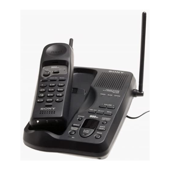
Sony SPP-A940 Service Manual
Hide thumbs
Also See for SPP-A940:
- Operating instructions manual (80 pages) ,
- Service manual (4 pages) ,
- Operating instructions manual (48 pages)

Related Manuals for Sony SPP-A940


Summary of Contents for Sony SPP-A940
- Page 1 SPP-A940 SERVICE MANUAL Canadian Model SPECIFICATIONS CORDLESS TELEPHONE MICROFILM...
-
Page 2: Table Of Contents
LES COMPOSANTS IDENTIFIÉS PAR UNE MARQUE ! SUR LES DIAGRAMMES SCHÉMATIQUES ET LA LISTE DES PIÈCES SONT CRITIQUES POUR LA SÉCURITÉ DE FONCTIONNEMENT. NE REMPLACER CES COMPOSANTS QUE PAR DES PIÈCES SONY DONT LES NUMÉROS SONT DONNÉS DANS CE MANUEL OU DANS LES SUPPLÉMENTS PUBLIÉS PAR SONY. - Page 3 SECTION 1 GENERAL LOCATION AND FUNCTION OF CONTROLS BASE UNIT 1 MIC (Microphone) 2 PLAY/STOP button 3 PAGE button 4 QUIC/SKIP button !∞ !¢ !§ !£ 5 ANSWER ON/OFF button !™ 6 ANSWER lamp !¶ 7 MENU button !¡ !• 8 VOLUME + button !ª...
- Page 4 This section is extracted from instruction manual. – 4 –...
- Page 5 – 5 –...
- Page 6 – 6 –...
- Page 7 – 7 –...
- Page 8 – 8 –...
- Page 9 – 9 –...
- Page 10 – 10 –...
- Page 11 – 11 –...
- Page 12 SECTION 2 DISASSEMBLY Note : Follow the disassembly procedure in the numerical order given. HANDSET SECTION 2-1. BATTERY PACK REMOVAL Battery pack (BP-T23) 3 Screws (+BTP 3x10) Lid, Battery case 2-2. CABINET (REAR), HAND REMOVAL Claws Cabinet (Rear), hand Claws Cabinet (Front), hand –...
- Page 13 2-3. HAND MAIN BOARD REMOVAL 1 Screw (+BTP 3x12) Antenna (ANT1) Spring Washer 3 Screws (+P 2x8) 2 Screw (+BTP 3x12) Hand main board Cabinet (Front), hand – 13 –...
-
Page 14: Circuit Operation
SECTION 3 CIRCUIT OPERATION FUNCTIONAL OVERVIEW 1.0 Introduction The basic function of the RF circuits on both handset and base is to provide a full duplex wireless link between the handset and base sections of the telephone. This is accomplished by setting up two simultaneous communications links between the handset and base RF sections. The RF receiver and transmitter circuitry essentially provide a link between the microphone and speaker in the handset to the telephone line in the base set. - Page 15 1.2 Block Diagram Both the handset and base RF modules follow the same block diagram shown below with only minor changes to incorporate the different transmit and receive frequencies. 2 POLE CERAMIC 1st RX AMP SAW FILTER 2nd RX AMP MIXER 10.7MHz CERAMIC IF AMP...
- Page 16 2.1.3 RX, TX Bandpass Filters The RX and TX bandpass filters provide two functions. The first is to effectively pass the correct frequencies to the RX and TX sections of the RF module. It is important especially for the RX section that these filters have a low insertion loss in order to ensure a low front end noise figure.
- Page 17 Receive Section 2.2.1 RX Amps and SAW Filter The purpose of the first RX amp is to provide enough gain that the noise figure of the RX section is fixed to a value as low as possible. It must provide a good 50Ω match to both the RX bandpass filter and the SAW filter. This amplifier must also have good power handling capability due to the limited filtering which precedes it.
- Page 18 A passive loop filter is employed to connect the synthesizer to the VCO. This tuning voltage may be observed at the ATE test point connector. This voltage should nominally be set to 2.0V for the base and 1.2V for the handset by adjusting the oscillator frequency with the variable capacitor.
- Page 19 BASE UNIT SECTION 3.1 Introduction This Machine is a 900MHz analog cordless telephone. The phone was developed with low cost and high performance in mind. The phone minimizes costs by using analog speech transmission and by utilizing a number of design innovations that reduce production costs. The speech transmission differs from our digital phones in that digital speech encoding and decoding does not occur in speech transmissions.
- Page 20 Sidetone cancellation is accomplished by taking the reflected transmit audio (the sidetone) and resistively combining it with out-of- phase transmit audio. In a real-world situation, the match between the line interface and the telephone line is not perfect. This slight mis-match results in some transmit audio being reflected back in the receive direction.
- Page 21 then leaves the RF module via the demodulator IC at about -16dBv (for a deviation of +/- 25kHz). From the RF module, the audio is then fed into a buffer amplifier where the audio is lowpass filtered and directed to both an audio channel and a data channel. The audio undergoes this split in directions after the buffer amplifier because both data and audio share the same circuits upto and including the buffer amplifier.
- Page 22 3.5.2 Data Communications The data is transmitted between the handset and base at 625 baud using Minimum Shift Keying (MSK) format. The two frequencies used in the keying are 300Hz and 600Hz which represents logic 0 and logic 1 respectively. A separate modem chip is not required in the design since the MCU generates and decodes all the data.
-
Page 23: Maintenance
In order to achieve a long stand-by time, the handset conserves power by “sleeping” when not in use and occasionally “waking-up”. In the “sleep” condition, the handset supplies power only to those circuits deemed essential for proper operation such as the microcontroller (MCU) and memory. - Page 24 receive audio level at the ear piece receiver. The receive audio level can vary from component tolerances and variations. Specifically, extra adjustment range has been implemented to compensate for variations in the receiver’s sensitivity. After the level control, the audio is passed to a final stage of amplification. The output of this amplifier can be taken differentially, but is taken single ended because of the amplifier’s adequate power capacity.
- Page 25 4.4.4 ATE Interface All connections to the ATE jig are facilitated by a single 10-pin header rather than a bed of nail which has been shown to have reliability problems. The ATE uses the header to access the signals required to complete a handset alignment. Handset to ATE communication is accomplished through a dedicated port on the MCU which is connected directly to a charge contact.
-
Page 26: Test Mode
SECTION 4 TEST MODE Test Mode Operation 1. Handset manual test mode user interface a) To enter test mode, press and hold # key for 2-3 seconds, then press 3 key twice with pressing # key. Emits happy tone. Turn on Tx, Rx at channel 6(1-10). - Page 27 SECTION 5 ADJUSTMENTS 5-1. BASE UNIT SECTION 4. TX DEVIATION Adjustment Procedure : • Perform the adjustment at 6CH (RX : 926.55MHz, TX : 1. Connect the modulation meter to ANTENNA point. 903.8MHz) by removing R1 as a rule. 2. Adjust the R135 for DEVIATION = 25kHz ± 1.0kHz reading on 1.
- Page 28 Connect Location : [BASE RF BOARD] (SIDE A) IC6 ( !• pin) : ANTENNA point DEMODULATION LEVEL Adjustment C116 R117 IC3 ( @§ pin) : 4.0MHz CLOCK REFERENCE Adjustment [BASE RF BOARD] (SIDE B) ATE TERMINAL RX AUDIO RX LOOP V TX LOOP V TX PWR ATE I/O...
-
Page 29: Handset Section
5-2. HANDSET SECTION 4. TX DEVIATION Adjustment Procedure : • Perform the adjustment at 6CH (RX : 903.8MHz, TX : 1. Connect the modulation meter to ANTENNA point. 926.55MHz) by removing R1 as a rule. 2. Adjust the R119 for TX DEVIATION= 25kHz ± 2kHz reading 1. - Page 30 Connect Location : [HAND MAIN BOARD] (SIDE A) ATE TERMINAL RX AUDIO RECEIVER + IC3 ( @§ pin) : ANTENNA point 4.0MHz CLOCK REFERENCE Adjustment RX AUDIO : QUAD-TUNE VOLTAGE Adjustment RECEIVER + : DEMODULATION LEVEL Adjustment Adjustment Location : R113 : DEMODULATION LEVEL Adjustment [HAND MAIN BOARD] (SIDE A) IC11...
- Page 31 SECTION 6 DIAGRAMS 6-1. EXPLANATION OF IC TERMINALS BASE UNIT SECTION IC3 LCC442350DW Pin No. Pin name Description ––––––––––––– RESET Reset terminal. External interrupt terminal. 3 – 8 PA7 – 2 Used for DTMF genaration. EEPROM SEL Chip select for EEPROM. PLL EN Chip select for PLL.
- Page 32 DSP SECTION IC6 TC88411AF Pin No. Pin name Description Serial data bus. Serial data bus. –––––––– External voice data memory write strobe. –––––––––– CAS1 External voice data memory column address strobe at DRAM connection. – Not used. – Not used. ANSWER ON/OFF LED drive.
- Page 33 Pin No. Pin name Description DVDD3 – Power supply terminal for digital (+5V). –––––––– Maskable interrupt input terminal. ––––––––– NON-Maskable interrupt input terminal (+5V). COL1 Key scan input terminal. COL0 Key scan input terminal. –––––––––––– WAIT Wait setting input terminal. AVSS1 –...
-
Page 42: Block Diagrams
IC BLOCK DIAGRAMS IC1 MC13156FB (HANDSET SECTION) Mixer DATA SLICER Bias Bias LIM AMP IF AMP IC1 MC13156DWR2 (BASE UNIT SECTION) Mixer DATA SLICER Bias Bias LIM AMP IF AMP – 60 –... - Page 43 IC2 TB31202FN (BASE UNIT SECTION) IC2 TB31202FN (HANDSET SECTION) SWITCH L. OSC PHASE COMPARATOR OUTPUT PROGRAMABLE –––––––– 32, 33 DIVIDER REFERENCE DIVIDER PROGRAMABLE –––––––– DIVIDER 32, 33 PHASE LOCK CONTROL COMPARATOR CIRCUIT OUTPUT IC5 BA10324AF (BASE UNIT SECTION) IC11 LP2953IM (HANDSET SECTION) IC5 BA10324AF (HANDSET SECTION) 16 GND INPUT...
-
Page 44: Exploded Views
SECTION 7 EXPLODED VIEWS NOTE : • -XX, -X mean standardized parts, so they may • The mechanical parts with no reference number have some difference from the original one. in the exploded views are not supplied. • Items marked “ * ”are not stocked since they are •... - Page 45 7-2. HANDSET SECTION ANT1 MIC1 Ref. No. Part No. Description Remark Ref. No. Part No. Description Remark 3-016-279-01 LID, BATTERY CASE 1-771-178-11 SWITCH, SHEET 3-016-288-01 HOLDER (MIC) 1-771-177-11 SWITCH, RUBBER KEY 3-016-290-01 TERMINAL (CHARGE:H/S) 3-016-287-01 TERMINAL, CHARGE 3-016-283-01 PANEL 3-016-291-01 TERMINAL (CHARGE:H/S) 3-016-280-01 CABINET (FRONT), HAND 3-016-285-01 HOLDER (BUZZER) 3-020-780-01 TAPE, CONDUCTIVE...
-
Page 46: Electrical Parts List
SECTION 8 BASE KEY BASE RF ELECTRICAL PARTS LIST NOTE : • SEMICONDUCTORS • Due to standardization, replacements in the In each case, u : µ , for example : The components identified by mark ! parts list may be different from the parts speci- uA.. - Page 47 BASE RF Ref. No. Part No. Description Remark Ref. No. Part No. Description Remark 1-162-923-11 CERAMIC CHIP 47PF C111 1-162-965-11 CERAMIC CHIP 0.0015uF 10% 1-164-004-11 CERAMIC CHIP 0.1uF C112 1-115-872-11 ELECT 2.2uF 1-164-004-11 CERAMIC CHIP 0.1uF C113 1-162-970-11 CERAMIC CHIP 0.01uF C115 1-162-968-11 CERAMIC CHIP...
- Page 48 BASE RF Ref. No. Part No. Description Remark Ref. No. Part No. Description Remark < COIL > 1-216-679-11 METAL CHIP 0.5% 1/10W 1-216-675-11 METAL CHIP 0.5% 1/10W 1-412-599-11 INDUCTOR CHIP 3.3uH 1-216-635-11 METAL CHIP 0.5% 1/10W 1-412-599-11 INDUCTOR CHIP 3.3uH 1-216-817-11 METAL CHIP 1/16W <...
- Page 49 BASE RF BASE TEL Ref. No. Part No. Description Remark Ref. No. Part No. Description Remark R110 1-216-848-11 METAL CHIP 180K 1/16W C134 1-115-872-11 ELECT 2.2uF R111 1-216-848-11 METAL CHIP 180K 1/16W C135 1-161-772-11 CERAMIC 0.1uF R112 1-216-844-11 METAL CHIP 1/16W C136 1-161-055-00 CERAMIC...
- Page 50 BASE TEL Ref. No. Part No. Description Remark Ref. No. Part No. Description Remark R121 1-249-412-11 CARBON 1/4W 1-162-923-11 CERAMIC CHIP 47PF R122 1-215-456-00 METAL 1/4W R123 1-215-436-00 METAL 4.3K 1/4W 1-162-923-11 CERAMIC CHIP 47PF R138 1-247-855-11 CARBON 1/4W 1-164-156-11 CERAMIC CHIP 0.1uF R139 1-249-427-11 CARBON...
- Page 51 HAND MAIN Ref. No. Part No. Description Remark Ref. No. Part No. Description Remark T-9416-153-1 TRANSISTOR MMBT3904LT1 1-216-841-11 METAL CHIP 1/16W T-9416-153-1 TRANSISTOR MMBT3904LT1 1-216-841-11 METAL CHIP 1/16W 1-216-841-11 METAL CHIP 1/16W T-9416-153-1 TRANSISTOR MMBT3904LT1 1-216-841-11 METAL CHIP 1/16W T-9416-153-1 TRANSISTOR MMBT3904LT1 T-9416-153-1 TRANSISTOR MMBT3904LT1 1-216-841-11 METAL CHIP 1/16W...
- Page 52 HAND MAIN Ref. No. Part No. Description Remark Ref. No. Part No. Description Remark 1-162-908-11 CERAMIC CHIP 0.25PF 50V 1-104-700-11 CERAMIC CHIP 0.027uF 1-162-923-11 CERAMIC CHIP 47PF 1-164-315-11 CERAMIC CHIP 470PF 1-162-923-11 CERAMIC CHIP 47PF 1-162-908-11 CERAMIC CHIP 0.25PF 50V 1-164-217-11 CERAMIC CHIP 150PF 1-162-923-11 CERAMIC CHIP...
- Page 53 HAND MAIN Ref. No. Part No. Description Remark Ref. No. Part No. Description Remark < TRIMMER > < RESISTOR > 1-141-374-11 CAP, TRIMMER 20PF 1-216-296-00 METAL CHIP 1/8W 1-141-374-11 CAP, TRIMMER 20PF 1-216-805-11 METAL CHIP 1/16W 1-216-835-11 METAL CHIP 1/16W <...
- Page 54 HAND MAIN Ref. No. Part No. Description Remark Ref. No. Part No. Description Remark R124 1-216-835-11 METAL CHIP 1/16W 1-219-570-11 METAL CHIP 1/16W R125 1-216-853-11 METAL CHIP 470K 1/16W 1-216-845-11 METAL CHIP 100K 1/16W 1-216-841-11 METAL CHIP 1/16W R126 1-216-864-11 METAL CHIP 1/16W 1-216-849-11 METAL CHIP 220K...
- Page 55 Ref. No. Part No. Description Remark ACCESSORIES & PACKING MATERIALS ******************************* 1-475-466-11 ADAPTOR, AC (AC-T24) 1-528-769-11 BATTERY PACK (BP-T23) 1-696-453-21 CORD (WITH MODULAR PLUG)(LINE) (15cm) 1-696-454-11 CORD (WITH MODULAR PLUG)(LINE) (215cm) 3-010-356-11 LABEL (MEMORY) 3-010-453-01 CASE, WALL HOOK 3-012-609-01 SPACER (WALL HOOK) 3-019-285-11 CARD, REMOTE CONTROL 3-860-766-21 MANUAL, INSTRUCTION (ENGLISH, FRENCH) 3-860-767-11 GUIDE, QUICK START...
- Page 56 SPP-A940 Sony Corporation 98E02042-1 9-925-737-31 Personal & Mobile Communication Company Printed in Japan © 1998.5 – 74 – Published by Quality Assurance Dept.
- Page 57 SPP-A940 Canadian Model Serial No. 0,101,999 and later SERVICE MANUAL SUPPLEMENT - 1 File this Supplement with the Service Manual. Subject : Change of DSP Board (ECN-CP800943)
-
Page 58: Printed Wiring Boards (Dsp Section)
SPP-A940 1. PRINTED WIRING BOARD (DSP SECTION) Semiconductor Location Ref. No. Location Note: • X : parts extracted from the component side. • : Through hole. • b : Pattern from the side which enables seeing. (The other layers' patterns are not indicated.) -
Page 59: Schematic Diagram (Dsp Section)
SPP-A940 2. SCHEMATIC DIAGRAM (DSP SECTION) Note: Waveform • All capacitors are in µF unless otherwise noted. pF: µµF 50 WV or less are not indicated except for electrolytics and tantalums. • All resistors are in Ω and W or less unless otherwise specified. -
Page 60: Electrical Parts List
SPP-A940 3. ELECTRICAL PARTS LIST NOTE : Ref. No. Part No. Description Remark Ref. No. Part No. Description Remark • Due to standardization, replacements in the • SEMICONDUCTORS When indicating parts by reference num- 8-719-018-89 PHOTO COUPLER LTV817-C 1-216-864-11 METAL CHIP 1/16W In each case, u : µ...