Table of Contents
Advertisement
Advertisement
Table of Contents

Related Manuals for Sony CDP-XA555ES


Summary of Contents for Sony CDP-XA555ES
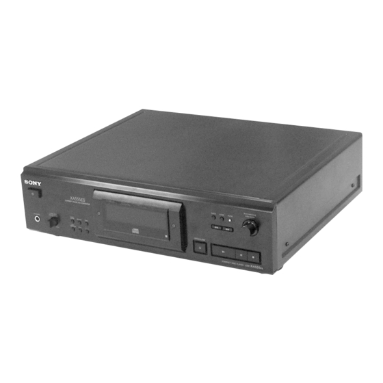
- Page 1 CDP-XA555ES SERVICE MANUAL AEP Model E Model Photo: Black Model Name Using Similar Mechanism CDP-XA50ES CDM32EB-12C (BLACK) CD Mechanism Type CDM32EN-12C (GOLD) Base Unit Type BU-12C Optical Pick-up Type KSS-273B/J1N SPECIFICATIONS – Continued on next page – COMPACT DISC PLAYER...
-
Page 2: Table Of Contents
• Do not touch the soldering iron on the same conductor of the OPERATION. REPLACE THESE COMPONENTS WITH circuit board (within 3 times). SONY PARTS WHOSE PART NUMBERS APPEAR AS • Be careful not to apply force on the conductor when soldering SHOWN IN THIS MANUAL OR IN SUPPLEMENTS PUB- LISHED BY SONY. -
Page 3: Servicing Notes
SECTION 1 SERVICING NOTES HOW TO PLAY CD WITH THE DISC TRAY NOTES ON HANDLING THE OPTICAL PICK-UP OPENED BLOCK OR BASE UNIT The laser diode in the optical pick-up block may suffer electro- To play a CD by this method, the screws that secure the SERVO static break-down because of the potential difference generated board to the chassis must be removed in advance. - Page 4 DISC PULLEY INSTALLING POSITION Note: The shaft on which the disc pulley is installed has a groove to determine the position (height). Install the disc pulley so that a setscrew can settle in this groove. disc pulley set screw disc pulley groove set screw (M2.6 ×...
- Page 5 SERVICE POSITION OF SERVO BOARD In servicing the SERVO board, erect the board as shown below. In this case, the CN201 and CN202 connectors are disconnected respectively, and accordingly the buttons on the front panel do not function. Therefore, use the Remote Commander for fundamental operations such as PLAY and STOP. Also, in performing the service under this condition, the stabilizer is not detected, so refer to “How to Operate the Set without Using Stabilizer”.
-
Page 6: General
SECTION 2 GENERAL LOCATION OF CONTROLS Front view Rear view 1 ! (power) switch qs Disc table 2 PLAY MODE button qd ERASE button 3 REPEAT button qf FILE button 4 TIME button qg EDIT/TIME FADE button 5 Fluorescent indicator tube display qh LINE OUT/PHONE LEVEL volume 6 m/M (forward/backward) button qj PHONES jack... - Page 7 Remote commander 1 SHUFFLE button 2 CONTINUE button 3 C.INDEX button 4 A.SPACE button 5 TIME button 6 Number button 7 >10 button 8 FILE button 9 ERASE button 0 REPEAT button qa H (play) button qs X (pause) button qd ./>...
-
Page 8: Disassembly
SECTION 3 DISASSEMBLY Note: Follow the disassembly procedure in the numerical order given. LOADING PANEL – BOTTOM VIEW – 2 tray 1 Open the tray turning the tapering screw driver to the arrow direction. 5 loading panel 3 two hexagon hole bolt (LID) 6 connector (CN292) 4 two screws... - Page 9 FRONT PANEL qd connector (CN203) qs connector (CN201) 3 screw (BVTT3 × 6) qa connector 4 harness (CN901) 6 screw 5 spacer (3 × 8) 7 bracket 6 screw 5 spacer (3 × 8) 7 bracket qg front panel 0 connector (CN202) 9 connector (CN461)
- Page 10 MECHANISM DECK (CDM32BN-12C) 1 connector 2 connector (CN91) (CN251) 9 two screws (BVTP3 × 6) 9 two screws (BVTP3 × 6) 3 connector (CN105) 4 connector (CN104) 5 connector (CN103) 6 connector (CN953) 0 mechanism deck 7 connector (CN935) 8 connector (CN914)
-
Page 11: Test Mode
SECTION 4 TEST MODE FLUORESCENT DISPLAY TUBE FULL ON AND – SERVO board (Conductor Side) – KEY CHECK MODE Procedure: 1. Connect TP(AFJ) and GND on the SERVO board with a lead wire. 2. Press button to turn the power ON. IC101 (AFJ) 3. - Page 12 AGING MODE This set has the Aging mode for operation check of the mechanism deck. • If a failure occurred The aging operation stops and a faulty status is displayed on the fluorescent display tube. • If no failure occurs The aging operation continues repeatedly.
-
Page 13: Electrical Adjustments
SECTION 5 ELECTRICAL ADJUSTMENTS Notes: RF signal waveform 1. CD block basically constructed to operate without adjustment. There- fore, check each item in order given. VOLT/DIV: 200 mV 2. Use YEDS-18 disc (Part No.: 3-702-101-01) unless otherwise indicated. TIME/DIV: 500 ns 3. - Page 14 5. Confirm that the oscilloscope waveform is symmetrical on the top and bottom in relation to 0 Vdc, and check this level. Traverse waveform + 1.5 level: 1.5 Vp-p – 0.5 6. After check, remove the lead wire connected in step 1. Skew Adjustment Note: Do not perform the skew adjustment when not using attached sta- bilizer to a set.
-
Page 15: Diagrams
CDP-XA555ES SECTION 6 DIAGRAMS 6-1. BLOCK DIAGRAM – SERVO Section – (Page 16) DIGITAL SIGNAL PROCESSOR, PRIORITY FOCUS/TRACKING/SLED ENCODER SERVO, EFM COMPARATOR DOUT (Page 16) IC101 CLOCK DIGITAL GENERATOR ASYO ADDRESS SUBCODE GENERATOR DETECTOR PROCESSOR INTEGRATOR Q101 SUBQ COMPARATOR RFAC... -
Page 16: Block Diagram - Main Section
CDP-XA555ES 6-2. BLOCK DIAGRAM – MAIN Section – WAVE SHAPER AUDIO AMP IC702 Q404 IC403(2/2) (Page 15) J710 DIGITAL OUT IC403 (1/2) MIX AMP COAXIAL – Q403 T710 JC701 FIXED OPTICAL (Page 15) OPTICAL OUT B– REGULATOR OPTICAL IC701 –20V... -
Page 17: Notes For Printed Wiring Board And Schematic Diagram
6-3. NOTES FOR PRINTED WIRING BOARD AND SCHEMATIC DIAGRAM • Circuit Boards Location Note on Printed Wiring Board: Note on Schematic Diagram: • X : parts extracted from the component side. • All capacitors are in µF unless otherwise noted. pF: µµF •... -
Page 18: Printed Wiring Board Servo Board (Component Side)
CDP-XA555ES 6-4. PRINTED WIRING BOARD – SERVO Board (Component Side) – • See page 17 for Circuit Boards Location. • Semiconductor Location Ref. No. Location D131 D132 IC110 Q171 Q172 Q181 Q182... -
Page 19: Printed Wiring Board - Servo Board (Conductor Side)
CDP-XA555ES 6-5. PRINTED WIRING BOARD – SERVO Board (Conductor Side) – • See page 17 for Circuit Boards Location. • Semiconductor Location Ref. No. Location (Page 35) (Page 25) (Page 35) D201 D202 D203 D204 IC101 IC102 IC103 IC104 IC105... -
Page 20: Schematic Diagram – Servo Board (1/2)
CDP-XA555ES 6-6. SCHEMATIC DIAGRAM – SERVO Board (1/2) – • See page 37 for Waveforms. • See page 38 for IC Block Diagrams. (Page 29) (Page 26) (Page 26) (Page 23) (Page 21) (Page 31) (Page 31) (Page 31) -
Page 21: Schematic Diagram - Servo Board (1/2)
CDP-XA555ES 6-7. SCHEMATIC DIAGRAM – SERVO Board (2/2) – • See page 37 for Waveforms. • See page 39 for IC Block Diagrams. (Page 36) (Page (Page 36) (Page 20) (Page 23) The components identified by mark 0 or dotted line with mark 0 are critical for safety. -
Page 22: Printed Wiring Boards - Bsl/Fl Relay/Flex Relay/Loading Motor/Loading Sw Boards
CDP-XA555ES 6-8. PRINTED WIRING BOARDS – BSL/FL RELAY/FLEX RELAY/LOADING MOTOR/LOADING SW Boards – • See page 17 for Circuit Boards Location. FLEXIBLE BOARD LOADING SW BOARD ( SLED ) S282 ( OUT ) LIMIT 1-653-918- LIMIT CN281 S283 (Page 19) -
Page 23: Schematic Diagram
CDP-XA555ES 6-9. SCHEMATIC DIAGRAM – BSL/FL RELAY/FLEX RELAY/LOADING MOTOR/LOADING SW Boards – (Page 21) (Page 20) (Page 33) -
Page 24: Printed Wiring Board - Audio Board (Component Side)
CDP-XA555ES 6-10. PRINTED WIRING BOARD – AUDIO Board (Component Side) – • See page 17 for Circuit Boards Location. -
Page 25: Printed Wiring Board - Audio Board (Conductor Side)
CDP-XA555ES 6-11. PRINTED WIRING BOARD – AUDIO Board (Conductor Side) – • See page 17 for Circuit Boards Location. (Page 35) (Page 19)(Page 35) (Page 28) (Page 19) (Page 19) (Page 28) (Page 28) (Page 28) (Page 28) (Page 28) -
Page 26: Schematic Diagram - Audio Board (1/2)
CDP-XA555ES 6-12. SCHEMATIC DIAGRAM – AUDIO Board (1/2) – • See page 37 for Waveforms. • See page 40 for IC Block Diagrams. (Page 20) (Page 20) (Page 21) (Page 36) (Page 27) (Page 36) (Page 36) -
Page 27: Schematic Diagram - Audio Board (2/2)
CDP-XA555ES 6-13. SCHEMATIC DIAGRAM – AUDIO Board (2/2) – • • See page 37 for Waveforms. See page 40 for IC Block Diagrams. (Page 29) (Page 29) (Page 29) (Page 29) (Page 29) (Page 29) (Page 29) (Page 26) (Page 29) -
Page 28: Printed Wiring Boards - Coax Out/D/O Sw/Line/Opt Out/Vr Boards
CDP-XA555ES 6-14. PRINTED WIRING BOARDS – COAX OUT/D/O SW/LINE/OPT OUT/VR Boards – • See page 17 for Circuit Boards Location. (Page 30) (Page 25) (Page (Page (Page 25) (Page 19) (Page 25) (Page 25) (Page 25)(Page 25) (Page 25) -
Page 29: Schematic Diagram - Coax Out
CDP-XA555ES 6-15. SCHEMATIC DIAGRAM – COAX OUT/D/O SW/LINE/OPT OUT/VR Boards – • See page 39 for IC Block Diagram. (Page 27) (Page 27) (Page 27) (Page 20) (Page 27) (Page 27) (Page 27) (Page 27) (Page 31) (Page 27) (Page 27) -
Page 30: Printed Wiring Boards - Key-L/Key-R Boards
CDP-XA555ES 6-16. PRINTED WIRING BOARDS – KEY-L/KEY-R Boards – • See page 17 for Circuit Boards Location. (Page 28) (Page 19) (Page 19) (Page 19) • Semiconductor Location – KYE-R Board – Ref. No. Location D871 D872 Q871 Q872 Q873... -
Page 31: Schematic Diagram - Key-L/Key-R Boards
CDP-XA555ES 6-17. SCHEMATIC DIAGRAM – KEY-L/KEY-R Boards – (Page 20) (Page 20) (Page 20) (Page 29) -
Page 32: Printed Wiring Board - Display Board
CDP-XA555ES 6-18. PRINTED WIRING BOARD – DISPLAY Board – • See page 17 for Circuit Boards Location. (Page 22) • Semiconductor Location (Conductor Side) Ref. No. Location IC801 IC802 IC803 IC804 Q801 Q802... -
Page 33: Schematic Diagram - Display Board
CDP-XA555ES 6-19. SCHEMATIC DIAGRAM – DISPLAY Board – • See page 41 for IC Block Diagram. (Page... -
Page 34: Printed Wiring Boards
CDP-XA555ES 6-20. PRINTED WIRING BOARDS – AC/POWER (Component Side) /SW Boards – • See page 17 for Circuit Boards Location. (Page 35) (Page 35) (Page 35) -
Page 35: Printed Wiring Board - Power Board (Conductor Side)
CDP-XA555ES 6-21. PRINTED WIRING BOARD – POWER Board (Conductor Side) – • See page 17 for Circuit Boards Location. • Semiconductor Location (Conductor Side) Ref. No. Location D910 D911 D912 D913 D914 D915 D916 D917 D918 D919 D920 D930 D931... -
Page 36: Schematic Diagram - Ac/Power/Sw Boards
CDP-XA555ES 6-22. SCHEMATIC DIAGRAM – AC/POWER/SW Boards – (Page 27) (Page 27) (Page 26) (Page 27) (Page 26) (Page 26) (Page 21) (Page 21) The components identified by mark 0 or dotted line with mark 0 are critical for safety. - Page 37 • Waveforms Board – SERVO Board – – AUDIO – 6 IC101 $∞ (LRCK) 1 IC201 #¡ (XTALI) 1 IC600 (BCKI) 5.2 Vp-p 5.2 Vp-p 4.8 Vp-p 4 MHz 22.7 µ s 474 ns 2 IC101 @§ (RFDC) 2 IC600 (LRCKI) 7 IC101 $¶...
- Page 38 • IC Block Diagrams – SERVO Board – IC101 CXD2545Q 61 – 51 DA16 EXCK DA12 LRCK WDCK SQSO PSSL SQCK MUTE SENS XRST DIRC ASYE SCLK DFSW ATSK AVDD ASYO DATA XLAT CLOK ASYI MIRR DFCT BIAS RFAC AVSS CLTV FILI LOCK...
- Page 39 IC106 TL712CPS-E05 IC205 LB1641 T.S.D O.C.P IN– OUT– MOTOR MOTOR DRIVE DRIVE OUT+ FWD/REV/STOP CONTROL LOGIC IC204 M51957AL – – VR Board – IC350 BA6208 MOTOR SWITCH DRIVE MOTOR SWITCH DRIVE...
-
Page 40: Audio Board
– AUDIO Board – IC401, 501 CXA8042AS IN2– I01+ I02– IN2+ I01– IN1+ SWITCHING I02+ IN1– CIRCUIT VCC2 GND2 VEE2 VCC1 CONSTANT REFERENCE VEE1 VREF CURRENT VOLTAGE CIRCUIT CIRCUIT CONTROL VCNT CIRCUIT CIREF GND1 RIREF IC600 CXD87629 64 63 62 61 60 59 58 57 56 55 54 53 52 51 50 49 48 47 46 45 44 43 42 41 SERIAL... -
Page 41: Display Board
IC601 CXD9521Q 64 63 62 61 60 59 58 57 56 55 54 53 52 51 50 49 48 47 46 45 44 43 42 41 5V I/O 5V I/O 3.3V/ NSCKSEL MCKSEL CTLVDD CLOCK CLKVDD MUTE GENERATOR LVCKO2 SYNC 3.3V/ R CH D/F LVCKO1... -
Page 42: Ic Pin Function Description
6-23. IC PIN FUNCTION DESCRIPTION SERVO BOARD IC101 CXD2545Q (DIGITAL SIGNAL PROCESSOR, FOCUS/TRACKING/SLED SERVO, EFM COMPARATOR) Pin No. Pin Name Description SRON Sled servo drive PWM signal output terminal Not used (open) SRDR Sled servo drive PWM signal (–) output to the BA6297AFP (IC102) SFON Sled servo drive PWM signal output terminal Not used (open) TFDR... - Page 43 Pin No. Pin Name Description WDCK Word clock signal (88.2 kHz) output terminal Not used (open) LRCK L/R sampling clock signal (44.1 kHz) output to the CXD8762Q (IC600) “L”: 48-bit slot serial data output when PSSL “H”: DA16 output when PSSL DATA (PSSL (pin rd) : fixed at “L”) Serial data output to the CXD8762Q (IC600) “L”: 48-bit slot bit clock signal output when PSSL “H”: DA15 output when PSSL...
- Page 44 Pin No. Pin Name Description SBSO Sub-code P-W serial data output terminal Not used (open) EXCK Sub-code P-W serial data reading clock signal input terminal Not used (fixed at “L”) SUBQ Sub-code Q data signal output to the system controller (IC201) SQCK Sub-code Q data reading clock signal input from the system controller (IC201) MUTE...
- Page 45 SERVO BOARD IC201 CXP84124-085Q (SYSTEM CONTROLLER) Pin No. Pin Name Description Address signal output to the static RAM (IC202) Address signal output to the static RAM (IC202) Address signal output to the static RAM (IC202) Address signal output to the static RAM (IC202) Address signal output to the static RAM (IC202) Address signal output to the static RAM (IC202) Address signal output to the static RAM (IC202)
- Page 46 Pin No. Pin Name Description Key input terminal (A/D input) A OPEN/CLOSE, N, X, x keys (S889 to S892) input Rotary encoder input terminal (A/D input) AMS L key (RV870) input Rotary encoder input terminal (A/D input) AMS l key (RV870) input ADJ/AFJ Setting terminal for the test mode “L”...
- Page 47 Main Ports SPDL-MUTE (pin qj) SENSER (pin wk) From the viewpoint of performance of the set, the disc must not The results of the detection of IC261 IS471F is output to this move nor sway when the disc table opens. These problems pin.
-
Page 48: Exploded Views
SECTION 7 EXPLODED VIEWS NOTE: • -XX and -X mean standardized parts, so they • Items marked “*” are not stocked since they The components identified by mark 0 or dotted line with mark may have some difference from the original are seldom required for routine service. - Page 49 4-220-319-01 BUTTON (MODE) (GOLD) A-4724-829-A KEY-R BOARD, COMPLETE 4-220-319-11 BUTTON (MODE) (BLACK) * 66 3-362-478-11 HOLDER (T), LED 4-942-568-41 EMBLEM (NO.5), SONY 4-221-258-01 BUTTON (FR) (GOLD) 4-221-262-01 KNOB (VOL) (GOLD) 4-221-258-11 BUTTON (FR) (BLACK) 4-221-262-11 KNOB (VOL) (BLACK) X-4951-807-1 BUTTON (PLAY) ASSY (BLACK)
- Page 50 (3) BACK PANEL SECTION supplied supplied supplied supplied supplied not supplied The components identified by mark 0 or dotted line with mark 0 are critical for safety. Replace only with part number specified. Ref. No. Part No. Description Remark Ref. No. Part No.
- Page 51 (4) CHASSIS SECTION T901 supplied supplied T902 supplied T903 CDM32BN-12C supplied not supplied supplied supplied supplied not supplied supplied The components identified by mark 0 or dotted line with mark 0 are critical for safety. Replace only with part number specified. Ref.
- Page 52 (5) MECHANISM DECK SECTION-1 (CDM32EB-12C) (BLACK) (CDM32EN-12C) (GOLD) not supplied BU-12C not supplied Ref. No. Part No. Description Remark Ref. No. Part No. Description Remark A-4724-901-A SERVO BOARD, COMPLETE 4-927-634-01 HOLDER (SP) * 702 4-968-903-01 SHAFT (MAIN) 4-948-375-01 SPRING (F), COIL 4-968-907-11 PANEL (DRAWER) 1-769-109-11 WIRE (FLAT TYPE) (12 CORE) 4-971-000-21 COVER (CD) (BLACK)
- Page 53 (6) MECHANISM DECK SECTION-2 (CDM32EB-12C) (BLACK) (CDM32EN-12C) (GOLD) M271 not supplied Ref. No. Part No. Description Remark Ref. No. Part No. Description Remark * 751 4-968-901-01 BEARING (MAIN) * 761 4-968-902-01 BEARING (SUB) 3-325-697-31 WASHER 1-653-905-11 LOADING SW BOARD 4-968-900-01 GEAR (LAST) X-4945-209-1 PULLEY (FIRST) ASSY 3-363-191-01 WASHER (BA) 4-968-905-01 BELT (CDM)
- Page 54 (7) BASE UNIT (BU-12C) 823 822 not supplied not supplied S21,S22 The components identified by mark 0 or dotted line with mark 0 are critical for safety. Replace only with part number specified. Ref. No. Part No. Description Remark Ref. No. Part No.
-
Page 55: Electrical Parts List
SECTION 8 AUDIO ELECTRICAL PARTS LIST NOTE: • Due to standardization, replacements in the • Items marked “*” are not stocked since they The components identified by mark 0 or dotted line with mark are seldom required for routine service. parts list may be different from the parts speci- 0 are critical for safety. - Page 56 AUDIO Ref. No. Part No. Description Remark Ref. No. Part No. Description Remark C611 1-126-929-11 ELECT 4700uF < CONNECTOR > C612 1-164-505-11 CERAMIC CHIP 2.2uF * CN401 1-564-505-11 PLUG, CONNECTOR 2P C613 1-119-793-11 ELECT 1000uF * CN402 1-564-505-11 PLUG, CONNECTOR 2P C614 1-119-793-11 ELECT 1000uF...
- Page 57 AUDIO Ref. No. Part No. Description Remark Ref. No. Part No. Description Remark L601 1-424-090-11 COIL, LINE FILTER R417 1-259-545-11 CARBON 1/2W L604 1-424-090-11 COIL, LINE FILTER L605 1-424-090-11 COIL, LINE FILTER R418 1-259-978-11 CARBON MELF 1/8W L607 1-424-090-11 COIL, LINE FILTER R419 1-259-983-11 CARBON MELF 1/8W...
- Page 58 AUDIO COAX OUT Ref. No. Part No. Description Remark Ref. No. Part No. Description Remark R583 1-216-037-00 METAL CHIP 1/10W R657 1-259-983-11 CARBON MELF 1/8W R584 1-216-037-00 METAL CHIP 1/10W R591 1-260-002-11 CARBON MELF 3.3K 1/8W R658 1-216-073-00 METAL CHIP 1/10W R601 1-216-001-00 METAL CHIP...
- Page 59 COAX OUT D/O SW DISPLAY FL RELAY FLEX RELAY KEY-L KEY-R Ref. No. Part No. Description Remark Ref. No. Part No. Description Remark R802 1-216-089-00 RES, CHIP 1/10W < JACK > R803 1-216-097-00 RES, CHIP 100K 1/10W ************************************************************** J710 1-507-567-71 JACK, PIN 1P (DIGITAL OUT COAXIAL) 1-653-906-11 FL RELAY BOARD <...
- Page 60 KEY-R LINE LOADING MOTOR LOADING SW OPT OUT POWER Ref. No. Part No. Description Remark Ref. No. Part No. Description Remark R882 1-249-417-11 CARBON 1/4W < RESISTOR > R883 1-249-419-11 CARBON 1.5K 1/4W R281 1-249-427-11 CARBON 6.8K 1/4W R884 1-249-421-11 CARBON 2.2K 1/4W R885...
- Page 61 POWER Ref. No. Part No. Description Remark Ref. No. Part No. Description Remark C937 1-119-793-11 ELECT 1000uF D950 8-719-210-21 DIODE 11EQS04-TA2B C938 1-127-764-21 FILM 10PF D951 8-719-210-21 DIODE 11EQS04-TA2B D952 8-719-210-21 DIODE 11EQS04-TA2B C939 1-126-017-11 ELECT 6800uF C940 1-109-857-11 ELECT 47uF D955 8-719-210-21 DIODE 11EQS04-TA2B...
- Page 62 POWER SERVO Ref. No. Part No. Description Remark Ref. No. Part No. Description Remark C134 1-163-109-00 CERAMIC CHIP 47PF R935 1-259-983-11 CARBON MELF 1/8W C135 1-163-121-00 CERAMIC CHIP 150PF R936 1-259-983-11 CARBON MELF 1/8W C136 1-163-121-00 CERAMIC CHIP 150PF R937 1-259-977-11 CARBON MELF 1/8W C137...
- Page 63 SERVO Ref. No. Part No. Description Remark Ref. No. Part No. Description Remark Q201 8-729-027-23 TRANSISTOR DTA114EKA-T146 * CN105 1-580-772-11 PIN, CONNECTOR (PC BOARD) 4P Q202 8-729-900-53 TRANSISTOR DTC114EKA-T146 CN201 1-580-774-11 PIN, CONNECTOR (PC BOARD) 6P CN202 1-580-775-11 PIN, CONNECTOR (PC BOARD) 8P <...
- Page 64 SERVO Ref. No. Part No. Description Remark Ref. No. Part No. Description Remark R155 1-216-097-00 RES, CHIP 100K 1/10W R220 1-216-073-00 METAL CHIP 1/10W R221 1-216-073-00 METAL CHIP 1/10W R156 1-216-085-00 METAL CHIP 1/10W R222 1-216-097-00 RES, CHIP 100K 1/10W R157 1-216-085-00 METAL CHIP 1/10W...
- Page 65 Ref. No. Part No. Description Remark Ref. No. Part No. Description Remark MISCELLANEOUS ************** 0 106 1-558-568-21 CORD, POWER 1-500-219-11 BEAD, FERRITE (CASE) 1-769-110-11 WIRE (FLAT TYPE) (26 CORE) * 706 1-654-005-11 FLEX RELAY BOARD 1-769-109-11 WIRE (FLAT TYPE) (12 CORE) 0 805 8-820-014-13 OPTICAL PICK-UP KSS-273B/J1N 1-653-918-11 PC BOARD, FLEXIBLE...
- Page 66 CDP-XA555ES Sony Corporation 9-928-966-11 99H0546-1 Home Audio Company Printed in Japan © 1999. 8 Published by Quality Assurance Dept.