Sign In
Upload
Manuals
Brands
Sel Manuals
Relays
411L
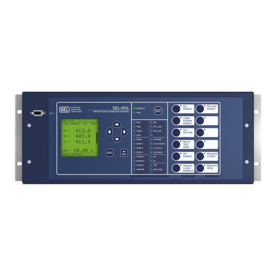
Sel 411L Line Differential Protection Manuals
Manuals and User Guides for Sel 411L Line Differential Protection. We have
1
Sel 411L Line Differential Protection manual available for free PDF download: Instruction Manual
Sel 411L Instruction Manual (1108 pages)
Protection and Automation System
Brand:
Sel
| Category:
Relays
| Size: 21.72 MB
Table of Contents
Table of Contents
3
List of Tables
9
List of Figures
23
Preface
35
Protection Manual
35
Section 1: Introduction and Specifications
43
Features
44
Figure 1.1 Functional Overview
44
Models and Options
47
Table 1.1 Communications Cards Options (Excluding EIA-232 Card)
49
Applications
50
Figure 1.2 Two-Terminal Application with Hot Standby Channel
51
Figure 1.3 Two-Terminal Application with In-Line Power Transformer and Hot Standby Channel
51
Figure 1.4 Two-Terminal Application with Hot Standby Channel and Tapped Load (Load Significantly Less than Through-Current)
51
Figure 1.5 Two-Terminal Application with Voltage Inputs
51
Figure 1.6 Terminal Master/Slave Application with Optional Third Communications Channel
52
Figure 1.7 Four-Terminal Ethernet Application
52
Table 1.2 Application Highlights
52
Specifications
55
Shared Configuration Attributes
63
Figure 2.1 Horizontal Front-Panel Template (A); Vertical Front-Panel Template (B)
65
Figure 2.2 Rear 4U Template, Fixed Terminal Block Analog Inputs
66
Table 2.1 Required Settings for Use with AC Control Signals
67
Figure 2.3 Standard Control Output Connection
68
Figure 2.4 Hybrid Control Output Connection
69
Figure 2.5 High-Speed, High-Current Interrupting Control Output Connection, INTE
70
Figure 2.6 High-Speed, High-Current Interrupting Control Output Connection, INTC
70
Figure 2.7 High-Speed, High-Current Interrupting Control Output Typical Terminals, INTE
71
Figure 2.8 Precharging Internal Capacitance of High-Speed, High-Current Interrupting Output Contacts, INTE
71
Figure 2.10 INTC I/O Interface Board (High Speed)
73
Figure 2.11 INTD I/O Interface Board (Standard)
73
Figure 2.12 INT7 I/O Interface Board
73
Figure 2.13 INTE I/O Interface Board
73
Figure 2.9 INT2 I/O Interface Board
73
Plug-In Boards
73
Table 2.2 I/O Interface Boards Control Inputs
74
Table 2.3 I/O Interface Boards Control Outputs
74
Jumpers
76
Figure 2.14 Jumper Location on the Main Board
77
Table 2.4 Main Board Jumpers
77
Figure 2.15 Major Jumper and Connector Locations on the Main Board
78
Figure 2.16 Main Components of the EIA-232 Board, Showing the Location of Serial Port Jumpers JMP1 and JMP2
79
Table 2.5 Serial Port Jumpers
79
Figure 2.17 Major Jumper and Connector Locations on the INT2 I/O Board
81
Figure 2.18 Major Jumper and Connector Locations on the INTC I/O Board
82
Figure 2.19 Major Jumper and Connector Locations on the INTE I/O Board
83
Figure 2.20 Major Jumper and Connector Locations on the INT7 I/O Board
84
Table 2.6 I/O Board Jumpers
85
Relay Placement
86
Connection
87
Figure 2.21 Chassis Dimensions
87
Figure 2.22 5U Rear, Main Board with EIA-422 Serial Communications Card in Bay 1, INT2 (200 Slot) and INTE (300 Slot) Interface Boards
88
Figure 2.23 4U Rear, Main Board with 1300 Nm IEEE C37.94 Fiber-Optic Serial Communications
89
Figure 2.24 5U Rear, Main Board with 850 Nm IEEE C37.94 Fiber-Optic Card in Bay 1, EIA-422
89
Figure 2.25 4U Rear, Main Board with EIA-422 Serial Communications Card in Bay
90
Figure 2.26 6U Rear, Main Board with EIA-422 Serial Communications Card in Bay
90
Figure 2.27 Rear-Panel Symbols
91
Figure 2.28 Screw Terminal Connector Keying
92
Figure 2.29 Rear-Panel Receptacle Keying
93
Table 2.7 Fuse Requirements for the Power Supply
94
Figure 2.30 Control Output OUT208 (INT2)
97
Table 2.8 Communications Options
99
Figure 2.31 Card Layout (Rear View of the Main Board)
100
Figure 2.32 Relay to Computer-D-Subminiature 9-Pin Connector
100
Table 2.9 Current Differential Communication Interface Options
101
Figure 2.34 Typical EIA-422 Interconnection
102
Figure 2.35 Typical G.703 Codirectional Interconnection
102
Figure 2.36 IEEE Standard C37.94 Fiber-To-Multiplexer Interface
103
Figure 2.37 1300 Nm Direct Fiber Connection
103
Figure 2.38 1550 Nm Direct Fiber Connection
103
Figure 2.39 Four 100BASE-FX Port Configuration
105
Figure 2.40 Four 10/100BASE-T Port Configuration
105
Figure 2.41 100BASE-FX and 10/100BASE-T Port Configuration
105
AC/DC Connection Diagrams
106
Figure 2.42 Typical External AC/DC Connections-Single Circuit Breaker
107
Figure 2.43 Typical External AC/DC Connections-Dual Circuit Breaker
108
87L Theory of Operation
110
Figure 3.1 Sampling and Transmitting Instantaneous Local Currents in the 87L Scheme (Breaker-And-A-Half Scheme)
113
Figure 3.2 Consolidating Currents in the 87L Scheme While Conserving the Channel Bandwidth
113
Figure 3.3 Traditional Alpha Plane Operating Characteristic for 87L Zone with Two Currents
115
Figure 3.4 AC Saturation Path of the External Fault Detector (Simplified)
118
Figure 3.5 Sharing the EFD Bits Among Relay Terminals
119
Figure 3.6 DC Saturation Path of the External Fault Detector (Simplified)
120
Figure 3.7 Illustration of Signal Processing for Line Charging Current Compensation
121
Figure 3.9 the Under- or Over-Compensated High-Frequency Components of the Charging Current Are Taken Care of by Boosting the Fundamental Frequency Restraining Term
123
Figure 3.10 a Combined Transformer and Line Zone Protected with a Single Line Differential Relay
124
Figure 3.11 Compensation for In-Line Transformers Is Performed at Early Stages of Signal Processing, Allowing the Rest of the Algorithm to Remain Unchanged
125
Figure 3.12 the Relay Allows Different Transformer Windings for each Measured CT (A) as Well as Dual-Breaker Terminations of the In-Line Transformer Windings (B)
126
Figure 3.13 Principle of Harmonic Restraint in the Generalized Alpha Plane Operating Characteristic
127
Figure 3.14 Illustration of the Channel-Based Synchronization Method
129
Figure 3.15 Application of Disturbance Detection in the Relay
133
Figure 3.16 Local (87DDL) and Remote (87DDR) Disturbance Detection Harmonized with the Stub Bus (ESTUB) and Test (87TEST) Conditions
133
Figure 3.17 Adaptive Disturbance Detector Algorithm
134
Figure 3.18 Disturbance Detection Guards against Multiple Problems Greatly Increasing Security
135
87L Differential Elements
136
Table 3.1 87L Current Input Configuration Settings
139
Table 3.2 87L Current Input Configuration Relay Word Bits
139
Table 3.3 87LP Phase Differential Elements Settings
140
Figure 3.19 87LP Phase Differential Element Logic
141
Table 3.4 87LP Phase Differential Elements Analog Quantities
141
Figure 3.20 Overcurrent Supervision Logic for Line Current Differential Elements (Use with Logic Diagrams in Figure 3.19, Figure 3.22, and Figure 3.23)
142
Figure 3.21 Alpha Plane Comparator Logic for Line Current Differential Elements (Use with Logic Diagrams in Figure 3.19, Figure 3.22, and Figure 3.23)
142
Table 3.5 87LP Phase Differential Elements Relay Word Bits
144
Table 3.6 87LQ Negative-Sequence Differential Element Settings
144
Table 3.7 87LQ Negative-Sequence Differential Element Analog Quantities
144
Figure 3.22 87LQ Negative-Sequence Differential Element Logic
145
Table 3.8 87LQ Negative-Sequence Differential Element Relay Word Bits
147
Table 3.9 87LG Zero-Sequence Differential Element Settings
147
Figure 3.23 87LG Zero-Sequence Differential Element Logic
148
Table 3.10 87LG Zero-Sequence Differential Element Analog Quantities
148
Figure 3.24 87OP Logic
150
Table 3.11 87LG Zero-Sequence Differential Element Relay Word Bits
150
Table 3.12 51S Operating Quantities Related to the Differential Current
152
Table 3.13 Stub Bus Settings
153
Table 3.14 Stub Bus Relay Word Bits
153
Figure 3.25 87DTT Transmit Logic
154
Figure 3.26 87DTT Logic
155
Table 3.15 87DTT Direct Transfer Tripping Settings
155
Table 3.16 87DTT Direct Transfer Tripping Relay Word Bits
155
Figure 3.27 Interaction between Debounce Timing and Fail-Safe Substitution in the User-Programmable 87L Bits Logic
157
Table 3.17 87L User-Programmable Communications Bits Settings (Serial Channels)
157
Table 3.19 User-Programmable Communications Bits Settings
159
Table 3.20 87L User-Programmable Communications Bits (Ethernet) Relay Word Bits
159
Figure 3.28 Providing Extra Security for Critical 87L Communications Bits Used for Unconditional Tripping (a Combination of Delay and Disturbance Detection Supervision)
161
Figure 3.29 Providing Extra Security for Critical 87L Communications Bits Used for Unconditional Tripping (Two Bits Used)
161
Figure 3.30 External Fault Detection Logic-AC Path and Reset
164
Figure 3.31 External Fault Detection Logic-DC Path
165
Figure 3.32 External Fault Detection Logic-Communications
166
Figure 3.33 External Fault Detection Logic-Usage in the 87L Elements
167
Table 3.21 External Fault Detection Relay Word Bits
167
Figure 3.34 Disturbance Detection Logic Responding to Local and Remote Signals, Stub Bus, and Test Mode
169
Figure 3.35 Disturbance Detection Logic Responding to Local Current and Voltage Signals
170
Figure 3.36 Disturbance Detection Logic Responding to Remote Currents
171
Figure 3.37 Adaptive Disturbance Detection Algorithm
172
Table 3.22 Adaptive Threshold Limits in the Adaptive Disturbance Detection Algorithm
172
Table 3.23 External Fault Detection Relay Word Bits
172
Table 3.24 Extended Security Alpha Plane Switchover Logic Settings
174
Figure 3.38 Extended Security Switchover Logic for the Alpha Plane Settings
175
Table 3.25 Extended Security Alpha Plane Switchover Logic Relay Word Bits
175
Table 3.26 Open CT Logic Settings
177
Figure 3.39 Open CT Detection Logic
178
Table 3.27 Open CT Logic Relay Word Bits
178
Figure 3.40 Line Charging Current Compensation Control Logic
181
Figure 3.41 Line Charging Current Calculations and Removal
182
Figure 3.42 Augmenting Restraint Terms for Finite Accuracy of Line Charging Current Compensation at Higher Frequencies
183
Table 3.28 Line Charging Current Compensation Settings
183
Table 3.29 Line Charging Current Compensation Relay Word Bits
183
Figure 3.43 Sample Three-Terminal Relay Application
186
Table 3.30 87L Applications with In-Line Transformers Winding Configuration Settings
189
Figure 3.44 Sample Three-Terminal Relay Application with In-Line Transformer
190
Table 3.31 Transformer Winding Compensation Matrices
191
Table 3.32 87L Applications with In-Line Transformers Harmonic Blocking and Restraining Settings
194
Table 3.33 Analog Quantities Related to Harmonic Blocking and Restraining
194
Figure 3.45 Harmonic Sensing Logic
195
Figure 3.46 Magnetizing Inrush and Overexcitation Blocking Logic
196
Table 3.34 87L Relay Word Bits Related to Harmonic Blocking and Restraining
197
Table 3.35 87LP Settings Specific to Applications with In-Line Transformers
198
Figure 3.47 87LP Logic in Applications with In-Line Transformers
199
Figure 3.48 87LP Alpha Plane Concept with Harmonic Restraint
200
Table 3.36 87LP Phase Differential Analog Quantities Specific to Applications with In-Line Transformers
200
Table 3.37 87L Relay Word Bits Related Unrestrained 87LP Operation
200
Figure 3.49 87LQ Logic in Applications with In-Line Transformers
202
Table 3.38 87L Applications with In-Line Transformers and Charging Current Compensation Settings
203
Figure 3.50 Level 1 Watchdog Monitor Diagram
206
Figure 3.51 Level 2 Watchdog Monitor Diagram
207
Table 3.39 87L Watchdog Relay Word Bits
207
Table 3.40 Current Line Differential Elements Operating Times (Cycles)-Serial Communication
207
Figure 3.52 Phase Elements Operating Times-Serial Communication
208
Figure 3.53 Negative-Sequence Elements Operating Times-Serial Communication
208
Figure 3.54 Zero-Sequence Elements Operating Times-Serial Communication
209
Figure 3.55 Phase Elements Operating Times-Ethernet Communication
209
Table 3.41 Current Line Differential Operating Times (Cycles)-Ethernet Communication
209
CT Selection Procedure
210
Figure 3.56 Negative-Sequence Elements Operating Times-Ethernet Communication
210
Figure 3.57 Zero-Sequence Elements Operating Times-Ethernet Communication
210
Figure 3.58 Power System Used for CT Selection Example
211
Current and Voltage Source Selection
214
Figure 3.59 Simulation of CT Transient Response on the 600:5 Tap
214
Figure 3.60 Current and Voltage Source Connections for the Relay
215
Figure 3.61 Main and Alternate Line Current Source Assignments
215
Figure 3.62 Combined Currents for Line Current Source Assignment
216
Figure 3.63 Breaker Current Source Assignments
216
Table 3.42 Available Current Source Selection Settings Combinations
216
Table 3.43 Available Current Source Selection Settings Combinations When ESS := y
217
Table 3.44 Available Current Source Selection Settings Combinations When ESS := y
217
Table 3.45 Available Voltage Source-Selection Setting Combinations
219
Table 3.46 ESS := N, Current and Voltage Source Selection
220
Figure 3.64 ESS := 1, Single Circuit Breaker Configuration
221
Figure 3.65 ESS := 2, Single Circuit Breaker Configuration
221
Table 3.47 ESS := 1, Current and Voltage Source Selection
221
Table 3.48 ESS := 2, Current and Voltage Source Selection
221
Figure 3.66 ESS := 3, Double Circuit Breaker Configuration
222
Table 3.49 ESS := 3, Current and Voltage Source Selection
222
Figure 3.67 ESS := 4, Double Circuit Breaker Configuration
223
Table 3.50 ESS := 4, Current and Voltage Source Selection
223
Figure 3.68 Tapped EHV Overhead Transmission Line
224
Figure 3.69 ESS := Y, Tapped Line
225
Table 3.51 ESS := Y, Tapped Line
225
Figure 3.70 ESS := Y, Single Circuit Breaker with Current Polarizing Source Tapped Power Transformer
226
Table 3.52 ESS := Y, Current Polarizing Source
226
Frequency Estimation
227
Polarizing Quantity for Distance Element Calculations
227
Table 3.53 VMEMC Relay Setting
227
Table 3.54 Frequency Measurement and Frequency Tracking Ranges
228
Figure 3.71 SEL-411L Alpha Quantity Calculation
229
Table 3.55 Frequency Estimation
229
Table 3.56 Voltage and Breaker Pole Correlation
229
Table 3.57 Frequency Estimation Outputs
230
Table 3.58 Time-Error Calculation Inputs and Outputs
230
Time-Error Calculation
230
Fault Location
231
Figure 3.72 Sample TEC Command Response
231
Figure 3.73 Sample TEC N Command Response
231
Figure 3.74 Relay Exchanging TW Peak Information Via 87L Communications Channel
233
Table 3.59 Traveling Wave Fault Location Settings
233
Figure 3.75 Summary Command Output Showing the TW Fault Location Result
234
Figure 3.76 Simplified Equivalent Network for Fault Location in Two-Terminal Lines
235
Figure 3.77 Fault Location on Three-Terminal Lines
236
Figure 3.78 Fault Location on Four-Terminal Lines
237
Table 3.60 Fault Location Triggering Elements
238
Table 3.61 Fault Type
239
Figure 3.79 Line with Two TAP Points
240
Table 3.62 Fault Location Settings for 2-, 3-, and 4-Terminal Lines with One TAP Point
240
Table 3.63 Fault Location Settings for 4-Terminal Line with Two TAP Points
241
Table 3.64 Fault Location Relay Word Bit
241
Open-Phase Detection Logic
242
Pole Open Logic
242
Table 3.65 Open-Phase Detection Relay Word Bits
242
Table 3.66 Pole Open Logic Settings
242
Table 3.67 EPO Setting Selections
243
Table 3.68 Pole Open Logic Relay Word Bits
243
Figure 3.80 Pole Open Logic Diagram
244
Loss-Of-Potential Logic
245
Figure 3.81 LOP Logic Process Overview
246
Table 3.69 LOP Logic Setting
246
Table 3.70 LOP Logic Relay Word Bits
246
Figure 3.82 LOP Logic
248
Fault Type Identification Selection Logic
249
Figure 3.83 Level 2 Watchdog Monitor Diagram
249
Table 3.71 Fault Type Identification Logic Settings
249
Table 3.72 FIDS Relay Word Bits
249
Ground Directional Element
250
Table 3.73 Directional Elements Supervising Ground Elements
250
Table 3.74 Ground Directional Element Settings
250
Table 3.75 Ground Directional Element Settings AUTO Calculations
251
Table 3.76 Ground Directional Element Enables
253
Figure 3.84 32Q and 32QG Enable Logic Diagram
254
Figure 3.85 32V and 32I Enable Logic Diagram
254
Table 3.77 Ground Directional Element Relay Word Bits
255
Figure 3.86 Best Choice Ground Directional Logic
256
Figure 3.87 Negative-Sequence Voltage-Polarized Directional Element Logic
257
Figure 3.88 Zero-Sequence Voltage-Polarized Directional Element Logic
257
Figure 3.89 Zero-Sequence Current-Polarized Directional Element Logic
258
Figure 3.90 Ground Directional Element Output Logic Diagram
258
Phase- and Negative-Sequence Directional Elements
260
Figure 3.91 32P, Phase Directional Element Logic Diagram
261
Figure 3.92 32Q, Negative-Sequence Directional Element Logic Diagram
261
Table 3.80 Phase- and Negative-Sequence Directional Elements Relay Word Bits
261
CVT Transient Detection
262
Directionality
262
Table 3.81 Zone Directional Settings
262
Figure 3.93 CVT Transient Detection Logic
263
Series-Compensation Line Logic
263
Table 3.82 CVT Transient Detection Logic Setting
263
Table 3.83 CVT Transient Detection Logic Relay Word Bit
263
Figure 3.94 Load-Encroachment Logic Diagram
264
Load-Encroachment Logic
264
Table 3.84 Series-Compensation Line Logic Relay Settings
264
Figure 3.95 Load-Encroachment Characteristics
265
Out-Of-Step Logic (Conventional)
265
Table 3.85 Load-Encroachment Logic Relay Settings
265
Table 3.86 Load-Encroachment Logic Relay Word Bits
265
Figure 3.96 OOS Characteristics
266
Table 3.87 OOS Logic Relay Settings
267
Table 3.88 OOS Logic Relay Word Bits
268
Figure 3.97 OOS Positive-Sequence Measurements
269
Figure 3.98 OOS Override Logic
269
Figure 3.99 OOS Logic Diagram
270
Figure 3.100 Open-Pole OSB Unblock Logic
271
Figure 3.101 Zero-Setting OOS Blocking Function
271
Out-Of-Step Logic (Zero Settings)
271
Figure 3.102 Swing Center Voltage Slope Detection Logic
273
Figure 3.103 Starter Zone Characteristic
274
Figure 3.104 Swing Signature Detector Logic
274
Figure 3.105 Swing Signature Detector Logic
276
Figure 3.106 Reset Conditions Logic
277
Figure 3.107 Type of Power Swings Detected by the DOSB Function
277
Figure 3.108 Dependable Power-Swing Block Detector Logic (EOOS = Y1)
278
Figure 3.109 Dependable Power-Swing Block Detector Logic (EOOS = Y)
279
Figure 3.110 Relay Word Bit DOSB Is the or Combination of DOSBY1 and DOSBY
279
Figure 3.111 Logic Diagram of the Three-Phase Fault Detector
280
Figure 3.112 Pole Open OOS Blocking Logic
280
Figure 3.113 I0/IA2 Angle Supervision During Pole-Open Situation
281
Figure 3.114 Blocking of the MAG Signal by the OSBA Fault Detection
281
Figure 3.115 Unblocking of the MAB Signal by the 67QUB Element
281
Table 3.89 Input/Output Combinations of the Pole-Open OOS Blocking Logic
281
Figure 3.116 Directional Element Signals 67QUBF and 67QUBR
282
Figure 3.117 OST Scheme Logic Resistive and Reactive Blinders
283
Figure 3.118 Logic that Determines Positive-Sequence Impedance Trajectory (EOOS = Y1)
284
Figure 3.119 Out-Of-Step Trip Logic (EOOS = Y1)
285
Mho Ground-Distance Elements
286
Table 3.90 Mho Ground-Distance Element Settings
287
Table 3.91 Mho Ground-Distance Elements Relay Word Bits
287
Figure 3.121 Zone 1 Mho Ground-Distance Element Logic Diagram
288
Figure 3.122 Zone 2 Mho Ground-Distance Element Logic Diagram
289
Figure 3.123 Zones 3, 4, and 5 Mho Ground-Distance Element Logic Diagram
290
Quadrilateral Ground-Distance Elements
290
Table 3.92 Differences between the Adaptive Right Resistance and the Existing
291
Table 3.93 Quadrilateral Ground-Distance Element Settings
291
Table 3.94 Quadrilateral Ground-Distance Elements Relay Word Bits
292
Figure 3.124 Zone 1 Quadrilateral Ground-Distance Element Logic Diagram
293
Figure 3.125 Zone 2 Quadrilateral Distance Element Logic Diagram
293
Figure 3.126 Zones 3, 4, and 5 Quadrilateral Ground-Distance Element Logic
294
Mho Phase Distance Elements
294
Table 3.95 Mho Phase Distance Element Settings
295
Table 3.96 Mho Phase Distance Elements Relay Word Bits
295
Figure 3.127 Zone 1 Mho Phase Distance Element Logic Diagram
296
Figure 3.128 Zone 2 Mho Phase Distance Element Logic Diagram
297
Figure 3.129 Zones 3, 4, and 5 Mho Phase Distance Element Logic Diagram
298
Quadrilateral Phase Distance Elements
299
Table 3.97 High-Speed and Conventional Element Directional Setting Summary
299
Figure 3.130 Quadrilateral Phase Distance Element Characteristic (TANGP = 0)
300
Figure 3.131 Quadrilateral Phase Distance Element Characteristic (TANGP = -10 Degrees)
301
Figure 3.132 Network to Determine Homogeneity
301
Figure 3.133 Tilt in Apparent Fault Impedance Resulting from Nonhomogeneity
302
Table 3.98 Quadrilateral Phase Distance Element Settings
303
Table 3.99 Quadrilateral Phase Distance Elements Relay Word Bits
303
Figure 3.134 Zone 1 AB Loop Conventional Quadrilateral Phase-Distance Element Logic
304
Figure 3.135 Zone 2 AB Loop Conventional Quadrilateral Phase Distance Element Logic
304
Figure 3.136 Zone 3, 4, and 5 AB Loop Conventional Quadrilateral Phase Distance Element Logic
305
Zone Time Delay
305
Table 3.100 Zone Delay Settings
306
Table 3.101 Zone Time Delay Relay Word Bits
306
Figure 3.137 Zone Timers
307
Instantaneous Line Overcurrent Elements
308
Table 3.102 Phase Overcurrent Element Settings
308
Table 3.103 Negative-Sequence Overcurrent Element Settings
309
Table 3.104 Residual Ground Overcurrent Element Settings
309
Table 3.105 Phase Instantaneous/Definite-Time Line Overcurrent Relay Word Bits
310
Table 3.106 Negative-Sequence Instantaneous/Definite-Time Line Overcurrent Relay Word Bits
310
Table 3.107 Residual Ground Instantaneous/Definite-Time Line Overcurrent Relay Word Bits
310
Figure 3.138 Phase Instantaneous/Definite-Time Overcurrent Elements
311
Figure 3.139 Residual Ground Instantaneous/Directional Overcurrent Elements
312
Figure 3.140 Negative-Sequence Instantaneous/Directional Overcurrent Elements
313
Selectable Time-Overcurrent Elements (51)
313
Table 3.108 U.S. Time-Overcurrent Equations
314
Table 3.109 IEC Time-Overcurrent Equations
314
Figure 3.141 U.S. Curves U1, U2, U3, and U4
315
Figure 3.142 U.S. Curve U5 and IEC Curves C1, C2, and C3
316
Figure 3.143 IEC Curves C4 and C5
317
Figure 3.144 Time-Overcurrent Logic
318
Table 3.110 Time-Overcurrent Operating Quantity List
319
Table 3.111 Settings for the Time-Overcurrent Elements
320
Figure 3.145 Over/Undervoltage Logic
321
Over/Undervoltage Elements
321
Table 3.112 Undervoltage Operating Quantity List
322
Table 3.113 Overvoltage Operating Quantity List
323
Switch-Onto-Fault Logic
325
Table 3.114 SOTF Settings
326
Table 3.115 SOTF Relay Word Bits
326
Figure 3.146 SOTF Logic Diagram
327
Communications-Assisted Tripping Logic
328
Figure 3.147 Required Zone Directional Settings
328
Table 3.116 ECOMM Setting
328
Directional Comparison Blocking Scheme
329
Table 3.117 DCB Settings
331
Table 3.118 DCB Relay Word Bits
331
Figure 3.148 DCB Logic Diagram
332
Permissive Overreaching Transfer Tripping Scheme
332
Table 3.119 POTT Settings
335
Table 3.120 POTT Relay Word Bits
336
Figure 3.149 Permissive Trip Receiver Logic Diagram
337
Figure 3.150 Directional Permissive Trip Receiver Logic Diagram
337
Figure 3.151 POTT Logic Diagram
338
Figure 3.152 POTT Scheme Logic (ECOMM := POTT3) with Echo and Weak Infeed
339
Directional Comparison Unblocking Scheme Logic
340
Figure 3.153 POTT Cross-Country Logic Diagram
340
Table 3.121 DCUB Settings
341
Table 3.122 DCUB Relay Word Bits
342
Figure 3.154 Permissive Trip Received Logic Diagram
343
Figure 3.155 DCUB Logic Diagram
344
Table 3.123 Additional Settings for Single-Pole Tripping (SPT)
345
Trip Logic
345
Table 3.124 Setting TULO Unlatch Trip Options
347
Table 3.125 Trip Logic Settings
349
Figure 3.156 Trip Logic Diagram
350
Figure 3.157 87L Single-Pole Trip Select Logic
352
Table 3.126 Trip Logic Relay Word Bits
352
Figure 3.158 Two Circuit Breakers Trip Logic Diagram
354
Circuit Breaker Failure Protection
355
Figure 3.159 Trip a Unlatch Logic
355
Figure 3.160 Trip During Open Pole
355
Figure 3.161 Scheme 1 Logic Diagram
356
Figure 3.162 Scheme 2 Three-Pole Circuit Breaker Failure Protection Logic
357
Figure 3.163 Scheme 2 Single-Pole Circuit Breaker Failure Protection Logic
358
Figure 3.164 Current-Supervised Three-Pole Retrip Logic
358
Figure 3.165 Current-Supervised Single-Pole Retrip Logic
359
Figure 3.166 no Current/Residual Current Circuit Breaker Failure Protection Logic Diagram
359
Table 3.127 Circuit Breaker Failure Protection Logic Settings
361
Table 3.128 Circuit Breaker Failure Relay Word Bits
362
Figure 3.167 Circuit Breaker Failure Seal-In Logic Diagram
364
Figure 3.168 Failure to Interrupt Load Current Logic Diagram
364
Figure 3.169 Flashover Protection Logic Diagram
365
Figure 3.170 Circuit Breaker Failure Trip Logic Diagram
365
Over/Underfrequency Elements
365
Figure 3.171 Over/Underfrequency Logic
366
Figure 3.172 Frequency Source Logic
366
Figure 3.173 Undervoltage Supervision Logic
366
Undervoltage Supervision Logic
366
Figure 3.174 Table Y12. Summary of the Valpha and 81UVSP Calculations
368
87L Communication and Timing
369
Table 3.129 87L Serial Interface Options
369
Figure 3.175 EIA-422 Three-Terminal, Master/Outstation Serial Application Using SEL-3094 Interface Converters
370
Figure 3.176 Four-Terminal Ethernet Application Using SEL ICON Multiplexers
370
Figure 3.177 Two Terminal Serial Application Using Redundant Channels
371
Table 3.130 Enable 87L Channel Settings
371
Table 3.131 Primary Serial Channel Setting
371
Table 3.132 Channel out of Service Settings
372
Table 3.133 Relay Address Settings
372
Table 3.134 Virtual Terminal over Serial Channel
372
Figure 3.178 EIA-422 Typical Connection
373
Table 3.135 EIA-422 Clock Settings
373
Figure 3.179 Back-To-Back EIA-422 Connection
374
Figure 3.180 Back-To-Back EIA-422 Connection Using the SEL-3094
374
Table 3.136 EIA-422 Configuration Settings and Cables
374
Table 3.137 SEL-3094 Settings
374
Figure 3.181 CCITT G.703 Typical Connection
375
Figure 3.182 Back-To-Back CCITT G.703 Connection
375
Table 3.138 CCITT G.703 Cables
375
Figure 3.183 C37.94, 850/1300 Nm Typical Connection
376
Table 3.139 Timing Source Settings
376
Figure 3.184 C37.94 Back-To-Back Connection
377
Table 3.140 Data Synchronization Settings
378
Table 3.141 Time Fallback Modes
379
Table 3.142 Ethernet Interface Options
379
Figure 3.185 Typical Ethernet Connections
380
Figure 3.186 Redundant Ethernet Connection
380
Table 3.143 Ethernet MAC Address Settings
380
Figure 3.187 Shared Ethernet Connection
381
Table 3.144 Ethernet VLAN Settings
381
Figure 3.188 Line Module of a Single ICON for Transporting Current Differential Data of Eight Relays to the SONET Network
384
Figure 3.189 Isolated Redundant Network Topology with Star Configuration and a Ring Topology with Dedicated, Managed Switches between Substations
385
Figure 3.190 Redundant Isolated Ring-Connected Network with Dedicated, Managed Switches
385
Figure 3.191 Isolated Ring-Connected Network with Dedicated, Managed Switches
386
Figure 3.192 Isolated, Star-Connected Network with Managed or Unmanaged Switches
386
Table 3.145 Impact of Network Performance on 87L Protection
386
Configuration, Monitoring, Alarming, and Logic for 87L Channels
387
87L Enable and Blocking Logic
388
Table 3.146 87L Enable and Blocking Settings
388
Figure 3.193 Enable Logic for the 87L Data Transmission and Differential Elements
389
Figure 3.194 Blocking Logic for the 87L Function
389
Table 3.147 87L Blocking Relay Word Bits
389
87L Active and Required Channel Logic
390
Table 3.148 Active 87L Channels as Determined by the Relay Part Number and the E87CH and 87PCH Settings
390
Figure 3.195 87Chprq Logic for the 2SS and 3SM 87L Configurations
391
87L Channel Synchronization Logic and Status
392
Figure 3.196 87Chprq Logic for the 2SD 87L Configuration
392
Table 3.149 Active and Required Channel Relay Word Bits
392
Table 3.150 Clock Offset Calculation Quality Relay Word Bits
394
Table 3.151 87L Absolute Time Quality Relay Word Bit
395
Table 3.152 87L Synchronization Method Settings
395
Figure 3.197 Synchronization Method Logic (P-Th Channel)
397
Figure 3.198 Quality of Synchronization Logic (P-Th Channel)
398
Figure 3.199 Quality of Synchronization Logic (87L Scheme)
398
Table 3.153 Channel Synchronization Method Relay Word Bits
398
87L Channel Monitoring and Alarming Logic
399
Table 3.154 87L Channel Alarm Settings
399
Figure 3.200 Maximum Round-Trip Delay Alarm Logic
400
Figure 3.201 Step Change in Round-Trip Delay Logic
401
Figure 3.202 Channel Asymmetry Alarm Logic
402
Figure 3.203 Lost Packet Alarm Logic
403
Figure 3.204 Noise Burst Alarm Logic
403
Figure 3.205 Momentary Channel Break Alarm Logic
403
Figure 3.206 Channel OK Status
404
Figure 3.207 Default Channel Alarm Logic
404
Table 3.155 87L Channel Alarm Relay Word Bits
404
87L Standby Channel Switchover Logic
405
Table 3.156 87L Channel Monitoring Analog Quantities
405
Figure 3.208 Principle of Hot Standby Channel Switching
406
Table 3.157 Hot Standby Logic Settings
406
Figure 3.209 Channel Switchover Logic (87HSB)
407
Table 3.158 Hot Channel Standby Logic Relay Word Bits
407
87L Time Fallback Logic
408
Table 3.159 Time Fallback Logic Setting
408
Table 3.160 Summary of Time Fallback Modes
408
Table 3.161 Merits of Time Fallback Modes Depending on the E87CH Application Setting
409
Figure 3.210 Request for Time Fallback from the P-Th 87L Channel
410
Figure 3.211 Time Fallback Mode 1 Logic
410
Figure 3.212 Time Fallback Mode 2 Logic
411
Figure 3.213 Time Fallback Modes 3 and 4 Logic
413
Table 3.162 Time Fallback Mode Relay Word Bits
413
87L Master, Outstation, and Loss of Protection Logic
414
Figure 3.214 87L Master (87MTR) Logic
415
Figure 3.215 87L Outstation (87SLV) Logic
415
87L Communications Report
416
Figure 3.216 87L Lost (87LST) Logic
416
Table 3.163 87L Status Relay Word Bits
416
Figure 3.217 COM 87L Report Layout
418
Table 3.164 COM87L Report Data Items
418
87L Channel Recorder
421
Protection Application Examples
423
Table 3.165 87L Channel Recorder Settings
423
Figure 3.218 500 Kv Overhead Transmission Line
424
Table 3.166 System Data-500 Kv Overhead Transmission Line and CT/PT Ratios
424
Table 3.167 Secondary Values
425
Figure 3.219 Channel Report During Commissioning Testing
428
Figure 3.220 345 Kv Overhead Tapped Line with In-Line Transformer
440
Table 3.168 System Data-345 Kv Overhead Transmission Line
440
Table 3.169 Secondary Impedances
441
Figure 3.221 CT Saturation Plot
445
Figure 3.222 Various Overcurrent Elements Used in this Example
447
Section 4: Autoreclosing and Synchronism-Check Autoreclosing
456
One-Circuit-Breaker Autoreclosing
458
Table 4.2 One-Circuit-Breaker Three-Pole Reclose Initial Settings
462
Table 4.3 One-Circuit-Breaker Single-Pole Reclose Initial Settings
462
Table 4.4 One Circuit Breaker Modes of Operation
462
Two-Circuit-Breaker Autoreclosing
464
Figure 4.2 Multiple Circuit Breaker Arrangement
469
Table 4.5 Dynamic Leader/Follower Settings
470
Figure 4.3 Multiple Circuit Breaker Arrangement
472
Table 4.6 Leader/Follower Selection
472
Table 4.7 Example One: Reset and 79CY3 States
472
Table 4.8 Example One: Lockout State
472
Table 4.10 Leader/Follower Selection
473
Table 4.9 Example One: Reset State after Reclaim Time
473
Table 4.11 Example Two: Initial Reset State
474
Table 4.12 Example Two: Final Reset State
474
Table 4.13 Leader/Follower Selection
475
Table 4.14 Example Three: Reset State
475
Table 4.15 Example Three: Three-Pole Cycle State
475
Figure 4.4 Leader/Follower Selection by Relay Input
476
Table 4.16 Example Three: Lockout State, BK1
476
Table 4.17 Leader/Follower Selection
476
Table 4.18 Two Circuit Breakers: Circuit Breaker BK1 out of Service
477
Table 4.19 Two-Circuit-Breaker Three-Pole Reclose Initial Settings
477
Table 4.20 Two-Circuit-Breaker Single-Pole Reclose Initial Settings
478
Table 4.21 Circuit Breaker BK1 Modes of Operation
478
Table 4.22 Circuit Breaker BK2 Modes of Operation
479
Table 4.23 Trip Logic Enable Options
480
Autoreclose Logic Diagrams
481
Figure 4.5 Circuit Breaker Pole-Open Logic Diagram
481
Figure 4.6 Line-Open Logic Diagram When E79 := y
481
Figure 4.7 Line-Open Logic Diagram When E79 := Y1
481
Figure 4.8 Single-Pole Reclose Enable
482
Figure 4.9 Three-Pole Reclose Enable
482
Figure 4.10 One Circuit Breaker Single-Pole Cycle State (79CY1)
483
Figure 4.11 One Circuit Breaker Three-Pole Cycle State (79CY3)
484
Figure 4.12 Two Circuit Breakers Single-Pole Cycle State (79CY1) When E79 := y
485
Figure 4.13 Two Circuit Breakers Single-Pole Cycle State (79CY1) When E79 := Y1
487
Figure 4.14 Two Circuit Breakers Three-Pole Cycle State (79CY3) When E79 := y
489
Figure 4.15 Two Circuit Breakers Three-Pole Cycle State (79CY3) When E79 := Y1
492
Manual Closing
494
Figure 4.16 Manual Close Logic
496
Voltage Checks for Autoreclosing and Manual Closing
497
Figure 4.17 Voltage Check Element Applications
498
Figure 4.18 Voltage Check Element Logic
499
Settings and Relay Word Bits for Autoreclosing and Manual Closing
499
Table 4.24 Autoreclose Logic Settings
499
Table 4.25 Autoreclose Logic Relay Word Bits
501
Figure 4.19 Partial Breaker-And-A-Half or Partial Ring-Bus Breaker Arrangement
503
Synchronism Check
503
Figure 4.20 Synchronism-Check Voltages for Two Circuit Breakers
504
Figure 4.21 Synchronism-Check Settings
505
Figure 4.22 Synchronism-Check Relay Word Bits
505
Table 4.26 Synchronism-Check Relay Word Bits
506
Figure 4.23 Example Synchronism-Check Voltage Connections to the Relay
507
Figure 4.24 Synchronism-Check Voltage Reference
508
Figure 4.25 Normalized Synchronism-Check Voltage Sources VS1 and VS2
509
Figure 4.26 Healthy Voltage Window and Indication
510
Figure 4.27 Synchronism-Check Enable Logic
510
Figure 4.28 "No Slip" System Synchronism-Check Element Output Response
512
Figure 4.29 "Slip-No Compensation" Synchronism-Check Element Output Response
513
Figure 4.30 "Slip-With Compensation" Synchronism-Check Element Output Response
515
Figure 4.31 Alternative Synchronism-Check Source 2 Example and Settings
517
Overview
519
Section 5: Settings
519
Table 5.1 Setting Categories and Appropriate Section
519
Alias Settings
520
Figure 5.1 Changing a Default Name to an Alias
521
Table 5.2 Default Alias Settings
521
Global Settings
522
Table 5.3 Global Settings Categories
522
Table 5.4 General Global Settings
522
Table 5.5 Global Enables
523
Table 5.6 Station DC1 Monitor (and Station DC2 Monitor)
523
Table 5.7 Control Inputs
523
Table 5.8 Interface Board #1 Control Inputs
523
Table 5.10 Settings Group Selection
524
Table 5.11 Data Reset Control
524
Table 5.9 Interface Board #2 Control Inputs
524
Table 5.12 Frequency Estimation
525
Table 5.13 Time-Error Calculation
525
Table 5.14 Current and Voltage Source Selection
525
Table 5.15 Synchronized Phasor Measurement
525
Table 5.16 Time and Date Management
526
Automation Free-Form SEL OGIC Control Equations
527
Protection Free-Form SEL OGIC Control Equations
527
Notes Settings
528
Output Settings
528
Table 5.19 Output Settings Categories
528
Table 5.20 Interface Board #1
528
Table 5.21 Interface Board #2
528
Front-Panel Settings
529
Table 5.22 Remote Analog Outputs
529
Table 5.24 87L Communication Bits Transmit Equations
529
Table 5.25 Front-Panel Settings Categories
529
Table 5.26 Front-Panel Settings
530
Table 5.27 Selectable Screens for the Front Panel
533
Table 5.28 Selectable Operator Pushbuttons
534
Table 5.29 Front-Panel Event Display
534
Table 5.30 Boolean Display Points
535
Table 5.31 Analog Display Points
535
Table 5.32 Local Control
535
Table 5.33 Local Bit SEL OGIC
535
Port Settings
536
Table 5.34 SER Parameters
536
Table 5.35 Port Settings Categories
536
Table 5.36 Protocol Selection
536
Table 5.37 Communications Settings
537
Table 5.38 SEL Protocol Settings
537
Table 5.39 Fast Message Read Data Access
537
Table 5.40 DNP3 Serial Protocol Settings
538
Table 5.41 DNP3 LAN/WAN Settings
539
Table 5.42 MIRRORED BITS Protocol Settings
540
Table 5.43 RTD Protocol Settings
541
Table 5.44 PMU Protocol Settings
541
Table 5.45 87L Port Settings
541
Table 5.46 87L Channel Monitoring Settings
542
Table 5.47 87L Communications Bits Debounce Time Delay-Serial Communication
542
DNP3 Settings-Custom Maps
543
Table 5.48 87L Communications Bits Debounce Time Delay-Ethernet Communication
543
Table 5.49 DNP3 Settings Categories
543
Table 5.50 DNP3 Object Default Map Enables
543
Table 5.51 Binary Input Map
543
Bay Settings
544
Table 5.52 Binary Output Map
544
Table 5.53 Counter Map
544
Table 5.54 Analog Input Map
544
Table 5.55 Analog Output Map
544
Table 5.56 Minimum and Maximum Fault Location
544
Table 5.57 Bay Settings
544
Table 6.1 SEL Software Solutions
547
Section 6: PC Software Overview
548
AC SEL ERATOR Quickset Setup
549
AC SEL ERATOR Quickset Terminal
551
Figure 6.1 Terminal Prompt
551
AC SEL ERATOR Quickset HMI
552
Figure 6.3 Virtual Relay Front Panel
552
Figure 6.4 Control Window
554
AC SEL ERATOR Quickset Settings
555
Figure 6.5 Settings Editor Selection
555
Figure 6.6 Setting the Part Number
556
Figure 6.7 Settings Driver
556
Figure 6.8 Opening Settings
557
Figure 6.9 Reading Settings
557
Figure 6.10 Relay Editor
558
Figure 6.11 Settings Editor Window
559
AC SEL ERATOR Quickset Event Analysis
561
Figure 6.13 Retrieving an Event History
562
Figure 6.14 Event Waveform Window
562
Figure 6.15 Sample Event Oscillogram
563
Figure 6.16 Retrieving Event Report Waveforms
563
Figure 6.17 Sample Phasors Event Waveform Screen
564
Figure 6.18 Sample Harmonic Analysis Event Waveform Screen
564
Figure 6.19 Sample Event Report Summary Screen
565
Figure 6.20 Sample Event Waveform Settings Screen
565
AC SEL ERATOR Quickset Settings Database Management
566
Figure 6.21 Database Manager
566
AC SEL ERATOR Quickset Help
567
Figure 6.22 Database Manager Copy/Move
567
Figure 7.1 Front Panel (12 Pushbutton Model)
569
Front-Panel Layout
569
Section 7: Front-Panel Operations
569
Figure 7.2 LCD Display and Navigation Pushbuttons
570
Figure 7.3 RELAY ELEMENTS Highlighted in MAIN MENU
571
Table 7.1 Front-Panel Inactivity Time-Out Setting
571
Table 7.2 Metering Screens Enable Settings
572
Figure 7.4 Sample ROTATING DISPLAY
573
Figure 7.5 Sample Alarm Points Screen
574
Figure 7.6 Deasserted Alarm Point
575
Table 7.3 SER Point Settings
575
Figure 7.7 Clear Alarm Point Confirmation Screen
576
Figure 7.8 no Alarm Points Screen
576
Figure 7.9 Alarm Points Data Loss Screen
576
Figure 7.10 Sample Display Points Screen
577
Table 7.4 Display Point Settings-Boolean
577
Table 7.5 Display Point Settings-Analog
578
Table 7.6 Display Point Settings-Boolean and Analog Examples
578
Figure 7.11 Fast Meter Display Points Sample Screen
580
Front-Panel Menus and Screens
580
Figure 7.12 Contrast Adjustment
581
Figure 7.13 Enter Password Screen
581
Figure 7.14 Invalid Password Screen
582
Figure 7.21 Events Menu Screen
587
Figure 7.23 SER Events Screen with Three Events
588
Figure 7.24 no SER Events Screen
588
Table 7.7 Front-Panel Pushbutton Functions While Viewing SER Events
588
Figure 7.26 RELAY ELEMENTS Screen
590
Figure 7.27 ELEMENT SEARCH Screen
590
Figure 7.28 LOCAL CONTROL Initial Menu
591
Figure 7.30 LOCAL CONTROL Example Menus
593
Table 7.8 Local Bit Control Settings
594
Figure 7.31 Local Bit Supervision Logic
595
Figure 7.32 OUTPUT TESTING Screen
596
Table 7.10 Settings Available from the Front Panel
596
Figure 7.35 Changing the ACTIVE GROUP
599
Figure 7.36 DATE/TIME Screen
599
Figure 7.41 RESET ACCESS LEVEL Screen
602
Figure 7.42 One-Line Diagram Screen
602
Figure 7.43 Sample Status Warning, Alarm Point Assertion, and Trip
603
Front-Panel Automatic Messages
603
Figure 7.44 Sample Status Warning in the LCD Message Area
604
Operation and Target Leds
604
Figure 7.45 Factory Default Front-Panel Target Areas
605
Table 7.11 Front-Panel Target Leds
605
Table 7.12 TIME Target LED Trigger Elements-Factory Defaults
606
Figure 7.46 Operator Control Pushbuttons and Leds
609
Front-Panel Operator Control Pushbuttons
609
Table 7.13 Operator Control Pushbuttons and Leds-Factory Defaults
609
Figure 7.47 Factory-Default Operator Control Pushbuttons
611
Section 8: Oscillography, Events, and SER Data Processing
614
Figure 8.1 Signal Processing in the Relay
615
Triggering Data Captures and Event Reports
616
Duration of Data Captures and Event Reports
617
Figure 8.2 Data Capture/Event Report Times
618
Table 8.1 Report Settings
618
Oscillography
619
Table 8.2 Event Report Nonvolatile Storage Capability
619
Figure 8.3 Sample Oscillogram
620
Figure 8.4 Sample COMTRADE .HDR Header File
621
Figure 8.5 COMTRADE .CFG Configuration File Data
622
Figure 8.6 COMTRADE Header File
624
Event Reports, Event Summaries, and Event Histories
626
Figure 8.7 Example Traveling Wave Oscillogram
626
Table 8.3 EVE Command
627
Table 8.4 EVE Command Examples
628
Figure 8.8 Fixed Analog Section of the Event Report
629
Table 8.5 Event Report Metered Analog Quantities
630
Table 8.6 87L Event Report Analog Quantities
630
Figure 8.9 Digital Section of the Event Report
632
Figure 8.10 Sample Digital Portion of the Event Report
633
Figure 8.11 Summary Section of the Event Report
635
Figure 8.12 Settings Section of the Event Report
636
Figure 8.13 Sample Compressed ASCII Event Report
637
Figure 8.14 Sample Event Summary Report
638
Table 8.7 Event Types
639
Figure 8.15 Sample Compressed ASCII Summary
640
Figure 8.16 Sample Event History
641
Figure 8.17 Sample Compressed ASCII History Report
642
Figure 8.18 Sample SER Report
643
Sequential Events Recorder (SER)
643
Table 8.10 SER Commands
644
Figure 8.19 Sample Compressed ASCII SER Report
645
Circuit Breaker Monitor
647
Section 9: Monitoring and Metering
647
Figure 9.1 Intelligent Circuit Breaker Monitor
648
Table 9.1 Circuit Breaker Monitor Configuration
648
Figure 9.2 Circuit Breaker Maintenance Curve (Manufacturer's Data)
650
Table 9.2 Circuit Breaker Maintenance Information-Example
650
Figure 9.3 Circuit Breaker Contact Wear Curve with Relay Settings
651
Figure 9.4 Trip Bus Sensing with Relay Input IN206
654
Figure 9.5 Mechanical Operating Time for Circuit Breaker 1 A-Phase
655
Figure 9.6 Electrical Operating Time for Circuit Breaker 1 A-Phase
657
Figure 9.7 Timing Illustration for Pole Scatter at Trip
658
Figure 9.8 Pole Discrepancy Measurement
660
Table 9.6 BRE Command
663
Figure 9.10 Breaker History Report
664
Figure 9.9 Breaker Report (for the most Recent Operation)
664
Figure 9.11 Circuit Breaker Preload Data
665
Figure 9.12 Typical Station DC Battery System
666
Station DC Battery System Monitor
666
Table 9.7 DC Monitor Settings and Relay Word Bit Alarms
667
Table 9.8 Example DC Battery Voltage Conditions
667
Table 9.9 Example DC Battery Monitor Settings-125 VDC for Vdc1 and 48 VDC for Vdc2
668
Figure 9.13 Ground Detection Factor Areas
669
Table 9.10 Example DC Battery Monitor Settings-AC Ripple Voltages
669
Figure 9.14 Battery Metering: Terminal
670
Table 9.11 Example DC Battery Monitor Settings-Ground Detection Factor (EGADVS := Y)
670
Metering
671
Table 9.12 MET Command
671
Table 9.13 Instantaneous Metering Quantities-Voltages, Currents, Frequency
673
Figure 9.15 Complex Power (P/Q) Plane
674
Table 9.14 Instantaneous Metering Quantities-Powers
674
Table 9.15 Instantaneous Metering Accuracy-Voltages, Currents, and Frequency
675
Table 9.16 Instantaneous Metering Accuracy-Power
675
Figure 9.16 Typical Current Measuring Accuracy
676
Table 9.17 Maximum/Minimum Metering Quantities-Voltages, Currents, Frequency, and Powers
676
Table 9.18 Demand and Peak Demand Metering Quantities-(LINE)
678
Table 9.19 Rolling Demand Calculations
679
Figure 9.18 Rolling Demand Metering
680
Figure 9.19 Demand Current Logic Outputs
681
Table 9.20 Demand Metering Settings
681
Table 9.21 Energy Metering Quantities-(LINE)
682
Figure 9.20 Response to the MET DIF Command
684
Figure 9.21 Response to the MET DIF Command When 87Kf, 87Kq and 87Kg Are Not Forced to Zero
685
Figure 9.22 Response to the MET DIF Command When 87Kf, 87Kq and 87Kg Are Forced to Zero
685
Table 9.22 Differential Metering Quantities
685
Figure 10.1 Serial Number Label
688
Section 10: Basic Relay Operations Inspecting a New Relay
688
Connecting and Applying Power
689
Figure 10.2 Power Connection Area of the Rear Panel
689
Table 10.1 Power Supply Voltage Inputs
689
Establishing Communication
690
Figure 10.3 PORT F, LCD Display, and Navigation Pushbuttons
690
Table 10.2 General Serial Port Settings
691
Changing the Default Passwords
692
Figure 10.4 Report Header
692
Figure 10.5 Access Level Structure
692
Table 10.3 Access Levels Commands and Passwords
693
Checking Relay Status
696
Figure 10.9 Checking Relay Status: Front-Panel LCD
699
Making Simple Settings Changes
699
Table 10.4 Settings Classes and Instances
700
Figure 10.10 Components of SET Commands
701
Table 10.5 Actions at Settings Prompts
702
Figure 10.11 Initial Global Settings
703
Table 10.6 Actions at Text-Edit Mode Prompts
704
Figure 10.12 Using Text-Edit Mode Line Editing to Set Display Points
706
Operating the Relay Inputs and Outputs
707
Figure 10.13 Terminal Display for PULSE Command
708
Figure 10.14 Front-Panel Menus for Pulsing OUT204
709
Figure 10.15 Password Entry Screen
710
Figure 10.16 Assigning an Additional Close Output: AC SEL ERATOR Quickset
712
Figure 10.17 Uploading Output Settings to the Relay
713
Readying the Relay for Field Application
713
Table 10.7 Control Inputs
713
Table 10.8 Communications Port Commands that Clear Relay Buffers
714
Section 11: Testing and Troubleshooting Testing Philosophy
716
Test Precautions
717
Table 11.4 Test Mode Output Supervision under Default Settings
718
Test Mode
718
Testing Features and Tools
720
Figure 11.1 87TOUT Logic
722
Table 11.5 UUT Database Entries for SEL-5401 Relay Test System Software-5 a Relay
724
Table 11.6 UUT Database Entries for SEL-5401 Relay Test System Software-1 a Relay
724
Relay Test Connections
725
Figure 11.3 Test Connections for the Multiterminal 87L Test
726
Figure 11.4 Test Connections for the Single-Terminal 87L Test
727
Figure 11.5 Test Connections for Protection Functions Other than 87L
728
Test Methods
728
Figure 11.6 Sample Targets Display on a Serial Terminal
729
Table 11.7 Phase Instantaneous Overcurrent Pickup
729
Figure 11.7 Viewing Relay Word Bits from the Front-Panel LCD
730
Checking Relay Operation
733
Figure 11.9 Uploading Output Settings to the Relay
733
Table 11.9 Tap Values of the Four Terminals
734
Figure 11.10 Single-Terminal Test
740
Figure 11.11 System under Loopback Testing
741
Figure 11.12 Negative-Sequence Instantaneous Overcurrent Element Settings: AC SEL ERATOR Quickset
743
Figure 11.13 Uploading Group 1 Settings to the Relay
743
Figure 11.14 ELEMENT SEARCH Screen
744
Figure 11.15 RELAY ELEMENTS Screen Containing Element 50Q1
744
Figure 11.16 Uploading Group 1 and Breaker Monitor Settings to the Relay
747
Table 11.10 Negative-Sequence Directional Element Settings AUTO Calculations
747
Figure 11.17 Finding Phase-To-Phase Test Quantities
749
Relay Self-Tests
752
Table 11.11 Alarm Relay Word Bits
752
Figure 11.18 Relay Status: AC SEL ERATOR Quickset HMI
753
Figure 11.19 Relay Status from a STATUS a Command on a Terminal
754
Figure 11.20 Compressed ASCII Status Message
754
Table 11.12 Overall Status Section
755
Table 11.13 Channel Configuration and Status Section
756
Relay Troubleshooting
757
Table 11.14 Channel Statistics Section
757
Table 11.15 Troubleshooting Procedures
758
Factory Assistance
760
Overview
761
Section 12: Bay Control
761
Circuit Breaker Status Logic
762
Disconnect Logic
762
Figure 12.1 Disconnect Switch Close Logic
763
Figure 12.2 Disconnect Switch Open Logic
763
Figure 12.4 Close Immobility Timer Logic
769
Figure 12.5 Open Immobility Timer Logic
769
Figure 12.6 Disconnect in Transition
772
Bay Control Front-Panel Operations
773
Figure 12.7 Bay Control One-Line Diagram
773
Table 12.1 Circuit Breaker and Disconnect Switch Definitions
774
Table 12.2 Circuit Breaker State Representations
775
Table 12.3 Disconnect Switch State Representations
775
Figure 12.8 Screens for Circuit Breaker Selection
777
Figure 12.9 Screens During a Pole-Discrepancy Condition
778
Figure 12.10 Screens for Disconnect Switch Selection
779
Figure 12.11 HMI Disconnect Operation Initiation
781
Figure 12.12 HMI Disconnect Operation in Progress
782
Figure 12.13 HMI Disconnect Operation Completed
783
Figure 12.14 Bay Control One-Line Diagram with Three-Position Disconnect Open
783
Table 12.4 Three-Position Disconnect Switch State Representations
784
Table 12.5 Three-Position Disconnect Switch Control Screen Status and Control Options
785
Figure 12.16 Bay Control One-Line Diagram with Three-Position Disconnect Closed In-Line
787
Figure 12.17 Example Application
788
Figure 12.18 Interactive Bay Control Setting Form
788
Figure 12.19 Illustration of Local and Remote Control Logic with Key Control
789
Figure 12.20 Busbar Label
790
AC SEL ERATOR Quickset SEL-5030 Software Bay Control Screens
791
Figure 12.21 Disconnect 1 Settings
791
Figure 12.22 Breaker 1 Settings
794
Figure 12.23 Break 1 Settings for a Single Pole Breaker
794
Figure 12.24 Analog Quantity Setting Form
795
Figure 12.25 Analog Quantity Setting Form
795
Figure 12.26 Analog Quantity Expression MDELE2
795
Figure 12.27 Analog Quantity Expression MDELE3
796
Figure 12.28 Bay Control Screen Selected for Rotating Display
796
Figure 12.29 Configuring PB1_HMI for Direct Bay Control Access
797
Predefined Bay Control One-Line Diagrams
797
Figure 12.30 Bay with Ground Switch (Option 1)
798
Figure 12.31 Bay Without Ground Switch (Option 2)
798
Figure 12.32 Tie Breaker Bay (Option 3)
799
Figure 12.33 Bay with Ground Switch (Option 4)
799
Figure 12.34 Bay Without Ground Switch (Option 5)
800
Figure 12.35 Transfer Bay (Option 6)
800
Figure 12.36 Tie Breaker Bay (Option 7)
801
Figure 12.37 Bay with Ground Switch (Option 8)
801
Figure 12.38 Bay Without Ground Switch (Option 9)
802
Figure 12.39 Bay with Ground Switch (Option 10)
802
Figure 12.40 Bay Without Ground Switch (Option 11)
803
Figure 12.41 Left Breaker Bay with Ground Switch (Option 12)
803
Figure 12.42 Right Breaker Bay with Ground Switch (Option 13)
804
Figure 12.43 Middle Breaker Bay (Option 14)
804
Figure 12.44 Left Breaker Bay Without Ground Switch (Option 15)
805
Figure 12.45 Right Breaker Bay Without Ground Switch (Option 16)
805
Figure 12.46 Bay with Ground Switch (Option 17)
806
Figure 12.47 Bay Without Ground Switch (Option 18)
806
Figure 12.48 Left Breaker Bay with Ground Switch (Option 19)
807
Figure 12.49 Left Breaker Bay Without Ground Switch (Option 20)
807
Figure 12.50 Right Breaker Bay with Ground Switch (Option 21)
808
Figure 12.51 Right Breaker Bay Without Ground Switch (Option 22)
808
Figure 12.52 Source Transfer (Option 23)
809
Figure 12.53 Throw-Over Bus Type 1 Switch (Option 24)
809
Figure 12.54 Throw-Over Bus Type 2 Switch (Option 25)
810
Figure 12.57 Different Types of Circuit Breakers and Disconnects
812
Figure 12.58 Different Types of Power System Components
812
Configuring High-Accuracy Timekeeping
813
Relay Configuration for High-Accuracy Timekeeping
813
Section 13: Time-Synchronized Measurements
813
Table 13.1 Relay Timekeeping Modes
814
Figure 13.1 TIME BNC Connector
815
Figure 13.2 Confirming the High-Accuracy Timekeeping Relay Word Bits
815
Figure 13.3 Results of the TIME Q Command
816
Table 13.2 Date/Time Last Update Sources
817
Figure 13.5 Setting OUT108 in AC SEL ERATOR Quickset
819
Figure 13.6 High-Accuracy Timekeeping Connections
820
Figure 13.7 Setting PMV64 with the Expression Builder Dialog Box
822
Fault Analysis
823
Figure 13.8 230 Kv Transmission Line System
823
Ogic
825
SEL OGIC Control Equation History
825
Separation of Protection and Automation Areas
826
Figure 14.1 Protection and Automation Separation
827
SEL OGIC Control Equation Programming
827
SEL OGIC Control Equation Setting Structure
830
Multiple Setting Groups
832
SEL OGIC Control Equation Capacity
834
SEL OGIC Control Equation Elements
835
Table 14.6 First Execution Bit Operation on Power-Up
836
Table 14.7 First Execution Bit Operation on Automation Settings Change
837
Table 14.8 First Execution Bit Operation on Protection Settings Change, Group Switch, and Source Selection
837
Table 14.9 SEL OGIC Control Equation Variable Quantities
837
Table 14.10 SEL OGIC Control Equation Math Variable Quantities
838
Table 14.11 Latch Bit Quantities
839
Table 14.12 Latch Bit Parameters
839
Table 14.13 Conditioning Timer Quantities
841
Table 14.14 Conditioning Timer Parameters
841
Figure 14.3 Conditioning Timer with Pickup and no Dropout Timing Diagram
842
Figure 14.4 Conditioning Timer with Pickup Not Satisfied Timing Diagram
842
Figure 14.5 Conditioning Timer with Dropout and no Pickup Timing Diagram
842
Figure 14.6 Conditioning Timer with Pickup and Dropout Timing Diagram
843
Table 14.15 Sequencing Timer Quantities
844
Table 14.16 Sequencing Timer Parameters
844
Figure 14.8 Sequencing Timer Timing Diagram
845
Table 14.17 Counter Quantities
846
Table 14.18 Counter Parameters
846
SEL OGIC Control Equation Operators
848
Table 14.19 Operator Precedence from Highest to Lowest
849
Table 14.20 Boolean Operator Summary
849
Table 14.21 Parentheses Operation in Boolean Equation
850
Table 14.22 NOT Operator Truth Table
850
Table 14.23 and Operator Truth Table
850
Figure 14.9 R_TRIG Timing Diagram
851
Table 14.24 or Operator Truth Table
851
Figure 14.10 F_TRIG Timing Diagram
852
Table 14.25 Comparison Operations
852
Table 14.26 Math Operator Summary
853
Table 14.27 Math Error Examples
853
Effective Programming
857
SEL-311 and SEL-351 Series Users
859
Description of Commands
863
Section 15: ASCII Command Reference
863
Table 15.1 2AC Command
863
Table 15.2 89CLOSE N Command
864
Table 15.3 89OPEN N Command
865
Table 15.4 AAC Command
865
Table 15.5 ACC Command
865
Table 15.6 BAC Command
865
Table 15.7 BNA Command
865
Table 15.10 BRE C a and BRE R a Commands
866
Table 15.11 BRE N H Command
866
Table 15.8 BRE N Command
866
Table 15.9 BRE N C and BRE N R Commands
866
Table 15.12 BRE N P Command
867
Table 15.13 CAL Command
867
Table 15.14 CAS Command
867
Table 15.15 CBR Command
867
Table 15.16 CBR TERSE Command
868
Table 15.17 CEV Command
868
Table 15.18 CEV ACK Command
868
Table 15.19 CEV C Command
869
Table 15.20 CEV L Command
869
Table 15.21 CEV Lyyy Command
869
Table 15.22 CEV N Command
869
Table 15.23 CEV NSET Command
870
Table 15.24 CEV NSUM Command
870
Table 15.25 CEV Sx Command
870
Table 15.26 CEV TERSE Command
871
Table 15.27 CEV Command Option Groups
871
Table 15.28 CHI Command
872
Table 15.29 CHI TERSE Command
872
Table 15.30 CLOSE N Command
872
Table 15.31 COM 87L Command
873
Table 15.32 COM C Command
873
Table 15.33 COM C C and COM C R Command
874
Table 15.34 COM C L Command
874
Table 15.35 COM RTC C Command
875
Table 15.36 COM RTC C C and COM RTC C R Command
875
Table 15.37 con Nn Command
876
Table 15.38 COPY Command
876
Table 15.39 CPR Command
877
Table 15.41 CSE TERSE Command
878
Table 15.42 CST Command
879
Table 15.43 CSU Command
879
Table 15.44 CEV ACK Command
879
Table 15.45 CSU MB Command
879
Table 15.46 CSU N Command
880
Table 15.47 CSU TERSE Command
880
Table 15.48 DATE Command
880
Table 15.49 DNA Command
881
Table 15.50 DNP Command
881
Table 15.51 ETH Command
881
Table 15.52 ETH C and ETH R Command
882
Table 15.53 EVE Command
882
Table 15.54 EVE a Command
882
Table 15.55 EVE ACK Command
883
Table 15.56 EVE C Command
883
Table 15.57 EVE D Command
883
Table 15.58 EVE L Command
883
Table 15.59 EVE Lyyy Command
884
Table 15.60 EVE N Command
884
Table 15.61 EVE NSET Command
884
Table 15.62 EVE NSUM Command
884
Table 15.63 EVE Sx Command
885
Table 15.64 EVE Command Option Groups
885
Table 15.65 EVE Command Examples
885
Table 15.66 EXIT Command
886
Table 15.67 FILE Command
886
Table 15.68 GOOSE Command
886
Table 15.69 Accessible GOOSE IED Information
887
Table 15.70 GROUP Command
888
Table 15.72 HIS Command
889
Table 15.73 HIS C and HIS R Commands
889
Table 15.74 HIS CA and HIS RA Commands
890
Table 15.75 ID Command
890
Table 15.77 LOOP Command
892
Table 15.78 LOOP DATA Command
892
Table 15.79 LOOP R Command
893
Table 15.80 MAC Command
893
Table 15.81 MAP 1 Command
893
Table 15.82 MAP 1 Region Command
894
Table 15.83 MET Command
894
Table 15.84 MET AMV Command
895
Table 15.85 MET ANA Command
895
Table 15.86 MET BAT Command
895
Table 15.87 MET D Command
896
Table 15.88 MET DIF Command
896
Table 15.89 MET E Command
897
Table 15.90 MET M Command
898
Table 15.91 MET PM Command
898
Table 15.92 MET PMV Command
899
Table 15.93 MET RMS Command
899
Table 15.94 MET RTC Command
900
Table 15.95 MET SYN Command
900
Table 15.96 MET T Command
900
Table 15.97 OAC Command
901
Table 15.98 OPEN N Command
901
Table 15.99 PAC Command
901
Table 15.100 PAS Level New_Password Command
902
Table 15.101 PAS Level DISABLE Command
902
Table 15.102 PING Command
902
Table 15.103 PORT P Command
903
Table 15.104 PORT KILL N Command
904
Table 15.105 PRO Command
904
Table 15.106 PUL Outnnn Command
905
Table 15.107 QUIT Command
905
Table 15.108 RTC Command
905
Table 15.109 SER Command
906
Table 15.110 SER C and SER R Commands
906
Table 15.111 SER CA and SER RA Commands
906
Table 15.112 SER CV or SER RV Commands
907
Table 15.113 SER D Command
907
Table 15.114 SET Command Overview
908
Table 15.115 SET a Command
908
Table 15.116 SET B Command
908
Table 15.117 SET D Command
909
Table 15.118 SET F Command
909
Table 15.119 SET G Command
909
Table 15.120 SET L Command
909
Table 15.121 SET M Command
910
Table 15.122 SET N Command
910
Table 15.123 SET O Command
910
Table 15.124 SET P Command
910
Table 15.125 SET R Command
911
Table 15.126 SET T Command
911
Table 15.127 SET TERSE Command Examples
911
Table 15.128 SHO Command Overview
912
Table 15.129 SHO a Command
912
Table 15.130 SHO B Command
912
Table 15.131 SHO D Command
913
Table 15.132 SHO F Command
913
Table 15.133 SHO G Command
913
Table 15.134 SHO L Command
913
Table 15.135 SHO M Command
914
Table 15.136 SHO N Command
914
Table 15.137 SHO O Command
914
Table 15.138 SHO P Command
914
Table 15.139 SHO R Command
915
Table 15.140 SHO T Command
915
Table 15.141 SNS Command
915
Table 15.142 STA Command
915
Table 15.143 STA a Command
916
Table 15.144 STA C and STA R Command
916
Table 15.145 STA S Command
916
Table 15.146 STA SC and STA SR Command
916
Table 15.148 SUM ACK Command
917
Table 15.149 SUM N Command
917
Table 15.150 TAR Command
918
Table 15.151 TAR ALL Command
918
Table 15.152 TAR R Command
918
Table 15.153 TAR X Command
919
Table 15.154 TEC Command
919
Table 15.155 TEST DB Command
920
Table 15.156 TEST DB off Command
920
Table 15.157 TEST DB2 Command
921
Table 15.158 TEST DB2 off Command
921
Table 15.159 TEST FM Command
922
Table 15.160 TEST FM dem Command
922
Table 15.161 TEST FM off Command
923
Table 15.162 TEST FM PEAK Command
923
Table 15.163 TIME Command
923
Table 15.164 TIME Q Command
924
Table 15.165 TIME DST Command
924
Table 15.166 TRI Command
924
Table 15.167 VER Command
925
Table 15.168 VIEW 1 Commands-Region
926
Table 15.169 VIEW 1 Commands-Register Item
926
Table 15.170 VIEW 1 Commands-Bit
927
Table 16.1 Alphabetical List of Relay Word Bits
929
Section 16: Relay Word Bits Alphabetic
930
Row List
967
Table 16.2 Row List of Relay Word Bits
967
Quantities Listed Alphabetically
1003
Section 17: Analog Quantities
1003
Table 17.1 Alphabetical List of Analog Quantities
1003
Quantities Listed by Function
1021
Table 17.2 Analog Quantities List by Function
1021
Appendix A: Firmware and Manual Versions
1037
Firmware
1037
Table A.1 Firmware Revision History
1038
Table A.2 Firmware Compatibility
1043
ICD File
1044
Sel Boot
1044
Table A.4 SEL-411L ICD File Revision History
1044
Manual
1045
Table A.5 Manual Revision History
1045
Appendix B: Firmware Upgrade Instructions
1051
Overview
1051
SEL Communications Processors
1052
Table B.1 Firmware Upgrade Files
1052
Upgrade Procedure
1052
Table 5.17 DNP3
1092
Table 6.5 Help
1092
Figure 6.12 Expression Builder
1094
Table 8.8 SUM Command
1094
Table 8.9 HIS Command
1094
Figure 11.2 Low-Level Test Interface
1098
Figure 9.17 Thermal Demand Metering
1098
Table 11.1 Acceptance Testing
1098
Table 11.2 Commissioning Testing
1098
Table 11.3 Maintenance Testing
1098
Table 15.147 SUM Command
1098
Advertisement
Advertisement
Related Products
Sel SEL-400 Series
Sel 421
SEL 551
Sel SEL-2664S
Sel SEL-300 Series
Sel SEL-300G
Sel SEL-311C-1
Sel SEL-311L
Sel SEL-321-1
Sel SEL-351A
Sel Categories
Relays
Controller
Control Systems
Control Unit
Transceiver
More Sel Manuals
Login
Sign In
OR
Sign in with Facebook
Sign in with Google
Upload manual
Upload from disk
Upload from URL